
Improvement of Mg-Doped GaN with Shutter-Controlled Process in Plasma-Assisted Molecular Beam Epitaxy


1
Center for Nanoscience and Nanotechnology, National Sun Yat-sen University, Kaohsiung 80424, Taiwan
2
Department of Physics, National Sun Yat-sen University, Kaohsiung 80424, Taiwan
*
Authors to whom correspondence should be addressed.
Crystals 2023, 13(6), 907; https://doi.org/10.3390/cryst13060907
Submission received: 14 May 2023
/
Revised: 28 May 2023
/
Accepted: 29 May 2023
/
Published: 1 June 2023
(This article belongs to the Special Issue Materials and Devices Grown via Molecular Beam Epitaxy)
Abstract
:Mg-doped GaN was grown by plasma-assisted molecular beam epitaxy (PAMBE) on a Fe-doped GaN template substrate by employing a shutter-controlled process. The transition from n-type to p-type conductivity of Mg-doped GaN in relation to the N/Ga flux ratio was studied. The highest p-type carrier concentration in this series was 3.12 × 1018 cm−3 under the most N-rich condition. By modulating the shutters of different effusion cells for the shutter-controlled process, a wide growth window for p-type GaN was obtained. It was found that the presence of Mg flux effectively prevents the formation of structural defects in GaN epi-layers, resulting in the improvement of crystal quality and carrier mobility.
1. Introduction
GaN, with its wide direct bandgap and superior physical properties, has broad applications in semiconductor technologies. For electronics, its high breakdown electric field and high electron saturation velocity enable the development of high-power and high-temperature devices [1,2]. Furthermore, its large spin splitting energy makes it suitable for application in spintronics [3,4]. For photonic devices, the ternary alloy of GaN and InN, i.e., InxGa1-xN, has a wide tunable direct band gap from 3.4 eV to 0.7 eV, covering the whole visible spectrum, and offers red–green–blue full-color materials for light-emitting diode or laser diode applications [5,6,7]. Particularly in such optoelectronic applications, a p-type compound layer is essential for device operation. Since p-type GaN was demonstrated by Amono et al. [8] using low-energy electron beam irradiation and by Nakamura et al. [9], who used a rapid thermal annealing process with Mg-doped GaN produced by metal–organic chemical vapor deposition (MOCVD), Mg is known as the most effective p-type dopant for GaN. However, it is still challenging to achieve p-type conductivity in GaN due to several obstacles for Mg-doping, such as high ionization energy (160–200 meV), high vapor pressure and low stick coefficient at growth temperature, and self-compensation with the native defects [10]. As a result, p-type GaN is often realized with high resistivity and low hole mobility in its electrical properties. Therefore, the understanding of how Mg is incorporated with a GaN layer in epitaxial growth is very crucial for the fabrication of GaN-based optoelectronic devices.
Although the knowledge of nitride materials and their related application (e.g., GaN-based blue LED) was well developed with chemical vapor deposition by S. Nakamura et al. [5,6], the optimized growth condition of Mg-doped GaN in molecular beam epitaxy (MBE) is still unclear. Apart from metal–organic chemical vapor deposition (MOCVD), which is the most popular technology in the fabrication of GaN, plasma-assisted molecular beam epitaxy (PAMBE) is another specific technology for the epitaxial growth of GaN layers under a specific hydrogen-free environment and allows for a lower temperature growth. Therefore, Mg-doped GaN can achieve p-type conductivity without any post-treatment as developed by S. Nakamura, and the growth temperature can be controlled below 650 °C [11,12]. In addition, MBE has been proven as a reliable approach for fabricating red–green–blue full-color nitride-based micro-LEDs with the growth of high indium content of InGaN or InAlN quantum wells under a low-temperature hydrogen-free environment [13,14,15]. Despite the prospect of MBE for the advantages of growing full-color nitride-based nanomaterials, the output performance for such optoelectronic devices is still poor because of contact fabrication, uniformity, or hole-carrier injection. Thus, a high-quality p-type GaN epi-layer can ensure the efficiency of hole-carrier injection and will improve the performance of optoelectronic micro-devices. To find the optimal growth condition in MBE, one can commonly vary either the growth temperature or flux ratio of III-V elements, or even apply a different shuttering technique, such as growth interruption or metal-modulated epitaxy (MME) [16,17,18]. The MME method is commonly applied in molecular beam epitaxy (MBE), where the shutters of effusion cells (Ga, Mg, or other metal sources) are periodically opened and closed, while the shutter of the N-plasma remains open throughout the entire growth procedure. This approach enables the epitaxial growth to cycle between Ga-rich and N-rich conditions due to the modulation of the shutters. Consequently, the MME method is consistently utilized in order to achieve a smooth surface and prevent the formation of metal droplets. It is critical to control Ga flux for the Mg-doping process since the Mg dopant will compete with the majority Ga atoms for bonding with nitrogen. However, p-type conductivity in Mg-doped GaN layers versus N/Ga flux ratio is still controversially discussed in N-rich, slightly Ga-rich, or extremely Ga-rich conditions [11,19,20,21]. In addition, polarity inversion has been observed in heavily doped situations, resulting in a decrease in hole concentration [22]. A large hole-carrier concentration above 1019 cm−3 using the MME method has been reported [12]. The growth mechanism derived from different results is still inconsistent, and the effective growth condition with Mg-doped GaN in MBE is still unclear. This paper aims to investigate the optimal growth condition of Mg-doped GaN in a PAMBE system. In order to clarify the growth mechanism and electrical transport properties of hole carriers concerning the N/Ga flux ratio, a series of growths with varying Ga flux and different shutter-controlled processes have been designed to modulate Mg and Ga flux at a fixed growth temperature, and the result has been discussed in this study.
2. Materials and Methods
The growth of Mg-doped GaN was performed using a PAMBE ultra-high vacuum system with a standard effusion cell for Ga evaporation (99.99995% purity), Mg (99.9995% purity), and ultra-high-purity nitrogen gas (99.9999% purity) supplied by a radio-frequency plasma source (Veeco model GEN 930) on 2 μm thick Fe-doped GaN template substrates which were pre-grown on a sapphire substrate by MOCVD. It was convenient to verify the growth parameters when we developed the Mg-doped GaN layers by the homo-epitaxy of PAMBE atop the MOCVD pre-grown GaN template substrate. Moreover, the Fe-ion acts as an acceptor which provides a deep-level trap with a GaN band structure in the pre-grown GaN substrate; therefore, the Fe-doped GaN template can be treated as a semi-insulator that has a very high resistivity and low carrier concentration. Using it as a substrate template, we could avoid the electrical channels being parallel to the as-grown GaN layer in Hall measurements. The 1 × 1 cm2 GaN-template substrates were degreased with acetone, isopropanol, and D.I. water in an ultrasonic bath for five minutes sequentially and then dried with nitrogen gas immediately before loading to the PAMBE system. In the beginning, the substrates were processed with a thermal treatment, out-gassed at 750 °C for 10 min in the ultra-high vacuum MBE system, and then Mg-doped GaN epi-layers were grown at 670 °C. The N flux was fixed at 9 × 10⁻⁶ torr which was determined by a beam flux monitor with the radio-frequency (RF) plasma power of 400 W. At the same time, the Ga flux was tuned to control the flux ratio as desired for different samples, which are shown in Table 1. Since the flux of Mg was very difficult to measure using the nude ion-gauge, we then set the temperature of the Mg effusion cell at 380 °C in this study. All the samples in Table 1 can be classified into two series according to the different growth techniques. Series 1 is the Ga-flux-dependent series, which is denoted as samples A to E in Table 1. The samples were grown in a standard epi-growth procedure in which the effusion cells and N-plasma supplied were set constant for sample growth. Ga flux was the only variable in this series. Samples that are denoted as F1, G1, F2, and G2 in Table 1 are classified in Series 2. In Series 2, samples were grown by using specific shutter-controlled processes. There are two different shuttering methods given in the processes. Samples F1 and G1 were grown using the conventional metal-modulated epitaxy (MME) method with a 10 s period of opening and closing. Samples F2 and G2 were grown using a method that involved modulating the Ga shutter only and keeping the Mg and the N-plasma shutter open throughout the entire growth procedure. In situ reflection high-energy electron diffraction (RHEED) was used to characterize the growth of thin films. The electrical properties of the samples were determined by Van der Pauw–Hall measurement at room temperature, with an applied magnetic field of 250 mT, and Au/Ni was annealed onto the samples as the ohmic contacts. The surface morphology was investigated using a scanning electron microscope (SEM) (JEOL JSM-6330TF). The structural properties and crystalline preferred orientations were characterized by high-resolution X-ray diffraction (XRD, Bede D1) using a SIEMENS D5000 X-ray diffractometer with a Cu anode. The optical properties of the samples were analyzed by micro-Raman in a backscattering configuration with a 633 nm laser (Horiba, Lab RAM HREvolution).
3. Results and Discussion
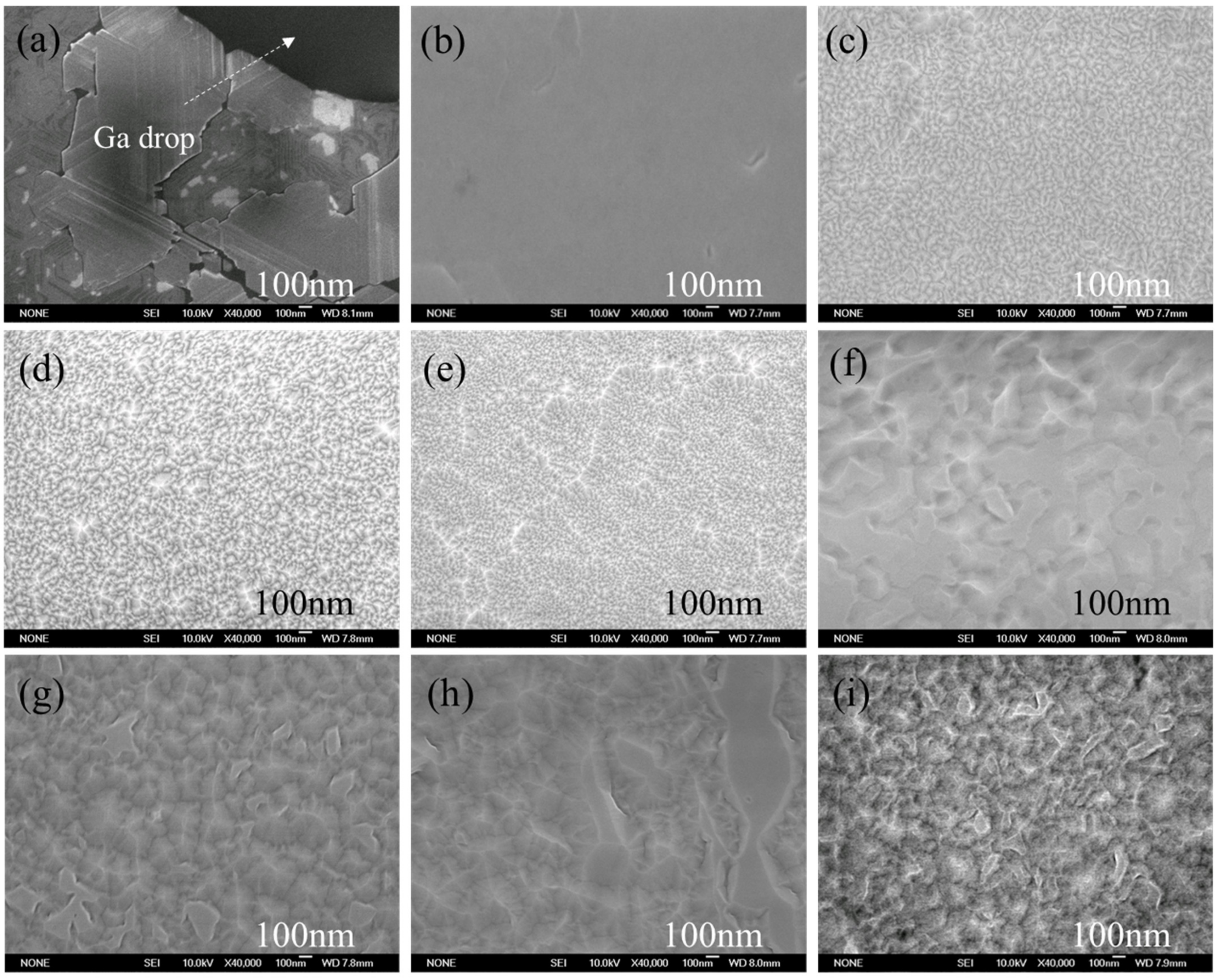
The in situ RHEED patterns after growth along of c-plane GaN for each sample are shown in Figure 1, and the SEM images are presented in Figure 2. The analysis of the morphology of sample A (flux ratio, 62) showed an excess of Ga drops on the surface in Figure 2a and yielded the dim streaky RHEED patterns in Figure 1a. With the increase in the flux ratio in samples C to E (N/Ga flux ratio, from 71 to 79), the samples presented bright and spotted RHEED patterns (Figure 1c–e) and correlated to a rough morphology under N-rich conditions, which can be observed in Figure 2c–e. These results reveal the signature of GaN grown by PAMBE: a smooth surface can be obtained under Ga-rich growth conditions, and a rough surface is presented under N-rich conditions [16]. The characterizations are ascribed to the high reactivity of the plasma source used in nitride-based MBE. Under the N-rich condition, the dwell time of Ga adatoms will be insufficient to migrate on the surface and leads to poor morphology. On the contrary, layer-to-layer growth takes place while the coverage of the Ga adlayer is in a Ga-rich condition and yields a smooth surface instead. The influence of flux ratio on the efficiency of Mg-doping was then investigated for samples A to E by Van der Pauw–Hall measurement. The results are listed in Table 2, and the sample thickness was estimated using the growth rate of our reactor. At a low flux ratio where the samples were still in a 2D growth mode (e.g., samples A and B), they exhibited n-type conductivity, while carrier concentration decreased as the Ga flux reduced. When the flux ratio increased to 71, the resistivity dramatically increased up to 9.36 × 101 Ω-cm, 3 orders in amplitude higher than those of samples A and B, and the p-type carrier was detected with the concentration of 2.15 × 1015 cm−3. More p-type hole carriers were produced as the growth condition varied toward a higher N/Ga flux ratio, and the highest value is 3.12 × 1018 cm−3 in this series with the mobility of 0.97 cm2/Vs (sample E). Under the Ga-rich growth condition, a large amount of Ga atoms will cover the surface, which can be confirmed by the RHEED pattern in Figure 1a. As a consequence, it is difficult for the Mg atom to replace the Ga atom for the synthesis of wurtzite crystal to produce a p-type dopant. As the Ga flux is reduced, it provides a greater possibility for the Mg atom to replace the Ga atom in the wurtzite structure, yielding p-type conductivity in the samples. Therefore, considering the growth temperature in the experiment, the N-rich condition is more favorable for the formation of a p-type dopant by Mg atoms. Although the highest hole mobility (31.08 cm2/Vs) was obtained in sample C in this series, the low carrier concentration did not meet the qualification for device operation. As the N/Ga flux ratio increased, enhancing the p-type carrier, a poor morphology was also acquired, which resulted in poor crystal quality and a decline in hole-carrier mobility.
To improve the surface morphology and ensure p-type conductivity in the samples, the shutter-controlled process was applied for the sample growth in Series 2. The detailed growth parameters can be found in Table 1. In a shutter-controlled process, the Ga flux is adjusted to extreme Ga-rich conditions, and the shutter is alternately switched between open and closed states, while the N-plasma shutter remains open. This sequence causes excess Ga droplets to accumulate on the surface when the Ga shutter is opened, while it allows the metal to migrate and form a flat surface when the Ga shutter is closed. Figure 1f–i show the RHEED patterns of the samples in Series 2. The patterns are all bright with a mixture of streaks and dots, indicating that the samples were free of droplets and exhibited 2D with minor 3D island growth. The SEM images in Figure 2f–i also showed a good agreement with the RHEED patterns. For samples F1 and F2, which were grown with a higher Ga flux equal to 1.80 × 10⁻⁷ torr, it was shown that the 3D structures demonstrated larger plateaus compared to samples G1 and G2. This observation suggested that the increase in Ga flux resulted in an increase in the diffusion distance of Ga atoms on the surface. Moreover, a higher hole concentration was achieved in samples F1 and F2 in the range of 1.42–2.70 × 1017 cm−3 as well, and it implied that the higher Ga flux during the shutter-controlled process can also enhance the incorporation of the p-type dopant. However, when comparing the Hall characterizations of samples F2 and G2 (i.e., the Mg effusion cell did not participate in the periodical shuttering and more Mg atoms were expected to be supplied during the growth process), it was found that these Mg atoms were not incorporated as the p-type dopants. As a consequence, samples F2 and G2 showed a similar amount of carrier concentration in comparison to samples F1 and G1, respectively. In contrast, there was a significant improvement in the hole-carrier mobility of samples F2 and G2 compared to the other samples of both series. It was also found that all the samples in Series 2 exhibited p-type conductivity, indicating that the shutter-controlled process covered a wide growth window of Ga flux in the range of 1.60–1.80 × 10⁻⁷ torr.
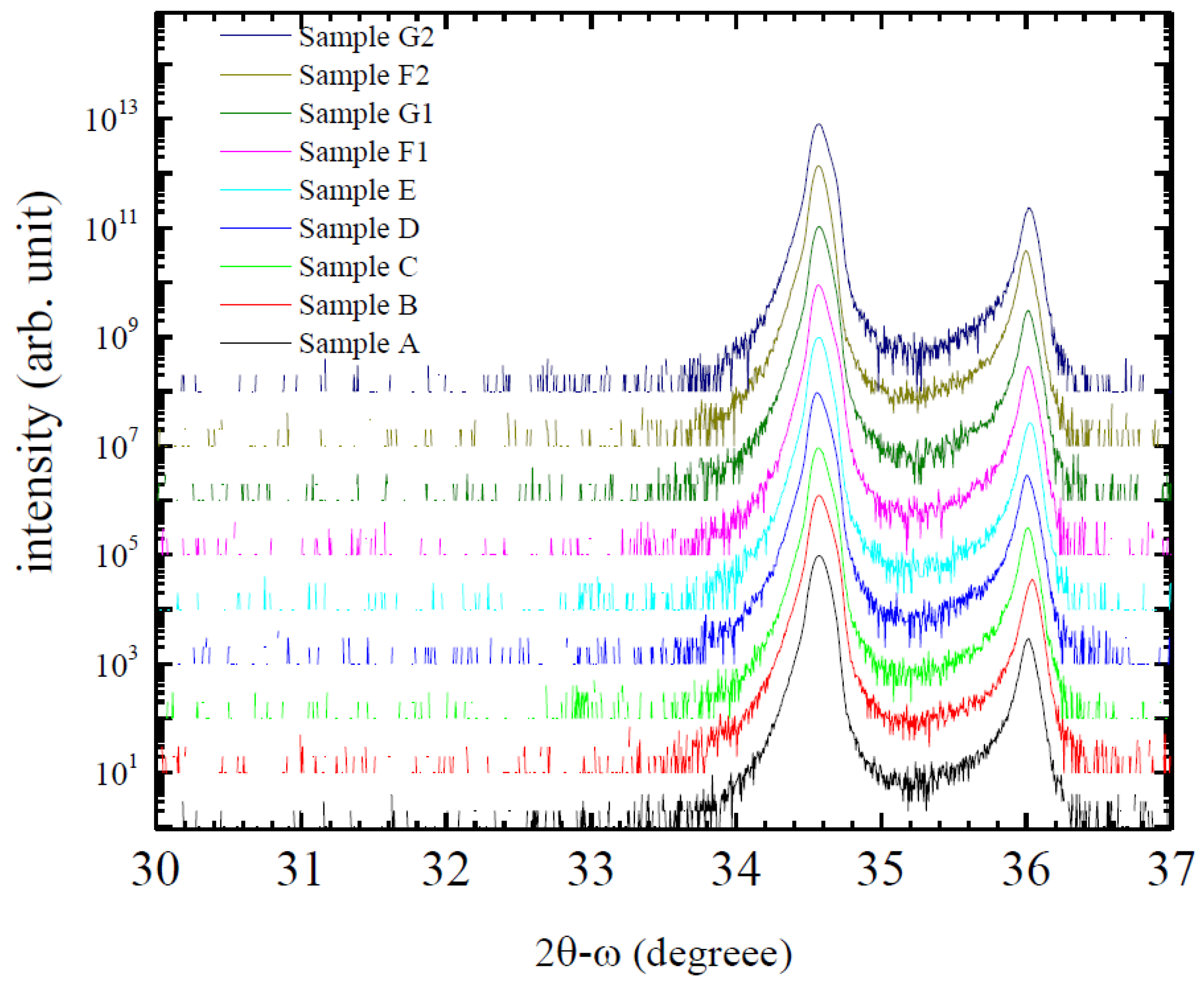
For further investigation, the structural and optical properties were analyzed by XRD and Raman scattering. In the XRD measurement, two peaks were obtained in the two theta-omega scanning, as shown in Figure 3. The peak at 34.5° is attributed to GaN (002), confirming the single crystalline nature of the samples, and the peak at 36.0° arose from AlN (002) which is from the original pre-grown GaN template (i.e., MOCVD grown GaN/AlN on sapphire substrate). Symmetric and asymmetric rocking curves for (002) and (102) were created to evaluate the structural defects, and the results are demonstrated in Figure 4. Figure 4a,b present the (002) and (102) rocking curves of the samples in Series 1, while Figure 4c,d present those of the samples in Series 2. The values of their full width at half maximum (FWHM) are presented in Table 3. The FWHM of the GaN (002) rocking curve is proportional to screw dislocation density. On the other hand, the FWHM of the GaN (102) rocking curve is proportional to the total dislocation density in the crystal, including both screw and edge dislocations [23]. Based on Table 3, the FWHM of the XRD rocking curves versus the N/Ga flux ratio for Series 1 was plotted (Figure 5). A V-valley trend versus the flux ratio for the FWHM of the GaN (102) rocking curve has been observed in Series 1, indicating that the sample grown at the N/Ga ratio of 71 had the best crystal quality in the series. This result was consistent with the Hall measurements. In the Hall measurements, sample C possesses the highest resistivity and low concentration, which means that the electrons, generated by the structural defects, can be almost neglected. Therefore, when the Mg dopant starts to incorporate with GaN, the hole carriers will not be compensated by the electrons. Thereby, the p-type conductivity can be detected even at a low concentration. In addition, the FHWM values of the samples in Series 2 are visualized as a bar chart in the inset of Figure 5. In Series 2, both GaN (002) and (102) rocking curves were broadened for the samples grown by the conventional MME method, i.e., samples F1 and G1. The best crystal quality was obtained in sample F2, which is verified by the FWHM of the GaN (102) rocking curve being 304 arc seconds. In semiconductors, the mobility of carriers depends on various factors of scattering, for instance, Coulomb, surface roughness, or defect scattering. It is evident that samples F2 and G2 exhibit lower threading dislocation (TD) density, as evaluated from the XRD rocking curves, which is associated with higher mobility as well. Since samples F2 and G2 were grown with only the Ga shutter modulated and the Mg source was supplied constantly with N-plasma, the surplus Mg atoms suppressed the formation of structural defects through mechanisms such as diffusion, adsorption, and desorption from the surface. Similar reactions such as the surface treatment of pre-grown gallium polishing in MBE have been discussed [24,25]. Figure 6 shows the Raman scattering spectra of the samples, where the backscattering method with the Raman configuration is presented. Using the confocal Raman probe system in this measurement, we can analyze the signal from different skin depths of the samples by adjusting the confocal pinhole size and the focus of the objective lens. The major scattering occurred at 570 cm−1 and 735 cm−1 and is attributed to the and A1(LO) modes of GaN. The sapphire substrate presented signals at 418 cm−1 and 750 cm−1 accompanied by minor peaks at 378 cm−1, 430 cm−1, and 449 cm−1 (Figure 6a) [26]. However, the peak at 660 cm−1 is very close to a different source, either the mode of AlN, the disorder of sapphire, or the vibration of Mg-N bonding [27,28,29,30,31]. In order to clarify these possibilities, the Raman sampling was performed by focusing on the surface only, and the results are shown in Figure 6b. Obviously, the signal from the deeper position of the sample became weaker or eliminated (Figure 6b), and the peaks at 660 cm−1 still survived, indicating the contribution from GaN. Kaschner et al. explained Mg-N vibration at 658 cm−1 in their experiment, which is very similar to the present results [29]. According to the black and red lines in Figure 6a,b, the signal of Mg-N bonding was absent in sample A but acquired in sample B. This confirms that the increase in the N/Ga flux ratio will be favorable for the replacement of Ga by the Mg dopant at the site of the cation. Despite the fact that the incorporation behavior of Mg occurred, sample B still exhibited n-type conductivity in the Hall measurement. This indicated that the amount of Mg doping in sample B was not enough to produce net hole carriers in the materials and was compensated by the presence of electrons in the background. Therefore, the hole concentration is relevant not only to the incorporation efficiency of Mg but also to the crystal quality and donor compensation.
4. Conclusions
Mg-doped GaN was grown by PAMBE on Fe-doped GaN templates. It was found that a transition of n-type to p-type conductivity was highly dependent on the N/Ga flux ratio in the standard epi-growth method with PAMBE. When the growth condition approached a N-rich environment, it created more opportunity for Mg to incorporate with GaN as hole carriers in the sample. The highest carrier concentration in this study reached 3.12 × 1018 cm−3 under the most N-rich condition. Moreover, a different shutter-controlled process was designed, and it provided a reliable and wide growth window for p-type GaN. In our investigation, the Mg flux in the shutter-controlled process not only participated as a p-type dopant during the growth, but also effectively prevented the formation of structural defects in GaN, leading to the improvement of hole-carrier mobility.
Author Contributions
Conceptualization, I.L.; methodology, Y.-C.W. and C.-D.T.; validation, Y.-C.W.; formal analysis, Y.-C.W.; investigation, Y.-C.W. and Y.-C.L.; resources, I.L. and T.-C.C.; data curation, Y.-C.W., Y.-C.L. and C.-D.T.; writing—original draft preparation, Y.-C.W.; writing—review and editing, I.L.; supervision, I.L.; project administration, I.L.; funding acquisition, I.L. and T.-C.C. All authors have read and agreed to the published version of the manuscript.
Funding
National science and technology council of Taiwan: 109-2124-M-110-002-.
Data Availability Statement
The data presented in this study are available on request from the corresponding author.
Acknowledgments
The project was supported by the National Science and Technology Council of Taiwan (NSTC, Taiwan) and the Center for NanoScience & NanoTechnology, National Sun Yat-sen University (Taiwan).
Conflicts of Interest
The authors declare no conflict of interest.
References
- Brillson, L.; Foster, G.; Cox, J.; Ruane, W.; Jarjour, A.; Gao, H.; Von Wenckstern, H.; Grundmann, M.; Wang, B.; Look, D.; et al. Defect Characterization, Imaging, and Control in Wide-Bandgap Semiconductors and Devices. J. Electron. Mater. 2018, 47, 4980–4986. [Google Scholar] [CrossRef]
- Li, L.; Alperin, J.; Wang, W.; Look, D.; Reynolds, D. High mobility AlGaN/GaN heterostructures grown by gas-source molecular beam epitaxy. J. Vac. Sci. Technol. B 1998, 16, 1275–1277. [Google Scholar] [CrossRef]
- Lo, I.; Tsai, J.K.; Yao, W.J.; Ho, P.C.; Tu, L.; Chang, T.C.; Elhamri, S.; Mitchel, W.C.; Hsieh, K.Y.; Huang, J.H.; et al. Spin splitting in modulation-doped AlxGa1−xN/GaN heterostructures. Phys. Rev. B 2002, 65, 161306. [Google Scholar] [CrossRef]
- Lo, I.; Pang, W.Y.; Chen, Y.L.; Hsu, Y.C.; Chiang, J.C.; Lin, W.H.; Chiu, W.T.; Tsai, J.K.; Chen, C.N. Spin-splitting in an AlxGa1−xN/GaN nanowire for a quantum-ring interferometer. Appl. Phys. Lett. 2008, 93, 132114. [Google Scholar] [CrossRef]
- Nakamura, S.; Mukai, T.; Senoh, M. Candela-class high-brightness InGaN/AlGaN double-heterostructure blue-light-emitting diodes. Appl. Phys. Lett. 1994, 64, 1687–1689. [Google Scholar] [CrossRef]
- Nakamura, S.; Pearton, S.; Fasol, G. The Blue Laser Diode; Springer: Berlin/Heidelberg, Germany, 2000. [Google Scholar]
- Ponce, F.A.; Bour, D.P. Nitride-based semiconductors for blue and green light-emitting devices. Nature 1997, 386, 351–359. [Google Scholar] [CrossRef]
- Amano, H.; Kito, M.; Hiramatsu, K.; Akasaki, I. P-type conduction in Mg-doped Gan treated with low-energy electron beam irradiation (LEEBI). Jpn. J. Appl. Phys. 1989, 28, L2112. [Google Scholar] [CrossRef]
- Nakamura, S.; Mukai, T.; Senoh, M.S.M.; Iwasa, N.I.N. Thermal annealing effect on p-type mg-doped gan films. Jpn. J. Appl. Phys. 1992, 31, L139–L142. [Google Scholar] [CrossRef]
- Kaufmann, U.; Schlotter, P.; Obloh, H.; Köhler, K.; Maier, M. Hole conductivity and compensation in epitaxial GaN: Mg layers. Phys. Rev. B 2000, 62, 10867. [Google Scholar] [CrossRef]
- Haus, E.; Smorchkova, I.; Heying, B.; Fini, P.; Poblenz, C.; Mates, T.; Mishra, U.; Speck, J. The role of growth conditions on the p-doping of GaN by plasma-assisted molecular beam epitaxy. J. Cryst. Growth 2002, 246, 55–63. [Google Scholar] [CrossRef]
- Namkoong, G.; Trybus, E.; Lee, K.K.; Moseley, M.; Doolittle, W.A.; Look, D.C. Metal modulation epitaxy growth for extremely high hole concentrations above 1019 cm−3 in GaN. Appl. Phys. Lett. 2008, 93, 172112. [Google Scholar] [CrossRef]
- Hsu, Y.-C.; Lo, I.; Shih, C.-H.; Pang, W.-Y.; Hu, C.-H.; Wang, Y.-C.; Tsai, C.-D.; Chou, M.M.C.; Hsu, G.Z.L. Green light emission by InGaN/GaN multiple-quantum-well microdisks. Appl. Phys. Lett. 2014, 104, 102105. [Google Scholar] [CrossRef]
- Tsai, C.-D.; Lo, I.; Wang, Y.-C.; Yang, C.-C.; Yang, H.-Y.; Shih, H.-J.; Huang, H.-C.; Chou, M.M.C.; Huang, L.; Tseng, B. Indium-Incorporation with InxGa1-xN Layers on GaN-Microdisks by Plasma-Assisted Molecular Beam Epitaxy. Crystals 2019, 9, 308. [Google Scholar] [CrossRef]
- Shih, H.-J.; Lo, I.; Wang, Y.-C.; Tsai, C.-D.; Lin, Y.-C.; Lu, Y.-Y.; Huang, H.-C. Growth and Characterization of GaN/InxGa1−xN/InyAl1−yN Quantum Wells by Plasma-Assisted Molecular Beam Epitaxy. Crystals 2022, 12, 417. [Google Scholar] [CrossRef]
- Tsai, J.-K.; Lo, I.; Chuang, K.-L.; Tu, L.-W.; Huang, J.-H.; Hsieh, C.-H.; Hsieh, K.-Y. Effect of N to Ga flux ratio on the GaN surface morphologies grown at high temperature by plasma-assisted molecular-beam epitaxy. J. Appl. Phys. 2004, 95, 460–465. [Google Scholar] [CrossRef]
- Moseley, M.; Lowder, J.; Villingsley, D.; Doolittle, W.A. Control of surface adatom kinetics for the growth of high-indium content InGaN throughout the miscibility gap. Appl. Phys. Lett. 2010, 97, 191902. [Google Scholar] [CrossRef]
- Sakaki, H.; Noda, T.; Hirakawa, K.; Tanaka, M.; Matsusue, T. Interface roughness scattering in GaAs/AlAs quantum wells. Appl. Phys. Lett. 1987, 51, 1934–1936. [Google Scholar] [CrossRef]
- Bhattacharyya, A.; Li, W.; Cabalu, J.; Moustakas, T.D.; Smith, D.J.; Hervig, R.L. Efficient p-type doping of GaN films by plasma-assisted molecular beam epitaxy. Appl. Phys. Lett. 2004, 85, 4956–4958. [Google Scholar] [CrossRef]
- Yang, Y.C.; Lee, P.Y.; Tseng, Y.H.; Lin, C.W.; Tseng, Y.T.; Cheng, K.Y. Mg incorporation in GaN grown by plasma-assisted molecular beam epitaxy at high temperatures. J. Cryst. Growth 2016, 439, 87–92. [Google Scholar] [CrossRef]
- Zhang, M.; Bhattacharya, P.; Guo, W.; Banerjee, A. Mg doping of GaN grown by plasma-assisted molecular beam epitaxy under nitrogen-rich conditions. Appl. Phys. Lett. 2010, 96, 132103. [Google Scholar] [CrossRef]
- Pezzagna, S.; Vennéguès, P.; Grandjean, N.; Massies, J. Polarity inversion of GaN(0001) by a high Mg doping. J. Cryst. Growth 2004, 269, 249–256. [Google Scholar] [CrossRef]
- Heying, B.; Wu, X.H.; Keller, S.; Li, Y.; Kapolnek, D.; Keller, B.P.; DenBaars, S.P.; Speck, J.S. Role of threading dislocation structure on the x-ray diffraction peak widths in epitaxial GaN films. Appl. Phys. Lett. 1996, 68, 643–645. [Google Scholar] [CrossRef]
- Bermudez, V.M.; Kaplan, R.; Khan, M.A.; Kuznia, J.N. Growth of thin Ni films on GaN(0001)-(1x1). Phys. Rev. B 1993, 48, 2436–2444. [Google Scholar] [CrossRef] [PubMed]
- Storm, D.; McConkie, T.; Hardy, M.; Katzer, D.; Nepal, N.; Meyer, D.; Smith, D. Surface preparation of freestanding GaN substrates for homoepitaxial GaN growth by rf-plasma MBE. J. Vac. Sci. Technol. B 2017, 35, 02B109. [Google Scholar] [CrossRef]
- Kadleíková, M.; Breza, J.; Veselý, M. Raman spectra of synthetic sapphire. Microelectron. J. 2001, 32, 955–958. [Google Scholar] [CrossRef]
- Gorczyca, I.; Christensen, N.E.; Peltzer y Blancá, E.L.; Rodriguez, C.O. Optical phonon modes in GaN and AlN. Phys. Rev. B 1995, 51, 11936–11939. [Google Scholar] [CrossRef]
- Kuball, M.; Demangeot, F.; Frandon, J.; Renucci, M.A.; Massies, J.; Grandjean, N.; Aulombard, R.L.; Briot, O. Thermal stability of GaN investigated by Raman scattering. Appl. Phys. Lett. 1998, 73, 960–962. [Google Scholar] [CrossRef]
- Kaschner, A.; Siegle, H.; Kaczmarczyk, G.; Straßburg, M.; Hoffmann, A.; Thomsen, C.; Birkle, U.; Einfeldt, S.; Hommel, D. Local vibrational modes in Mg-doped GaN grown by molecular beam epitaxy. Appl. Phys. Lett. 1999, 74, 3281–3283. [Google Scholar] [CrossRef]
- Wang, L.; Chua, S.; Sun, W. Raman scattering and photoluminescence of Mg-implanted GaN films. Phys. Status Solidi (B) 2001, 228, 449–452. [Google Scholar] [CrossRef]
- Harima, H. Properties of GaN and related compounds studied by means of Raman scattering. J. Phys. Condens. Matter 2002, 14, R967. [Google Scholar] [CrossRef]
Figure 1.
In situ RHEED patterns of samples (a) A, (b) B, (c) C, (d) D, (e) E, (f) F1, (g) G1, (h) F2, and (i) G2.
Figure 1.
In situ RHEED patterns of samples (a) A, (b) B, (c) C, (d) D, (e) E, (f) F1, (g) G1, (h) F2, and (i) G2.

Figure 2.
SEM images of samples (a) A, (b) B, (c) C, (d) D, (e) E, (f) F1, (g) G1, (h) F2, and (i) G2.
Figure 2.
SEM images of samples (a) A, (b) B, (c) C, (d) D, (e) E, (f) F1, (g) G1, (h) F2, and (i) G2.

Figure 3.
XRD results of all the samples; the y-axis has been offset for comparison.

Figure 4.
Rocking curves of XRD omega scan for (a) GaN (002) and (b) GaN (102) of Series 1 and (c) GaN (002) and (d) GaN (102) of Series 2. The y-axis has been offset for comparison.
Figure 4.
Rocking curves of XRD omega scan for (a) GaN (002) and (b) GaN (102) of Series 1 and (c) GaN (002) and (d) GaN (102) of Series 2. The y-axis has been offset for comparison.
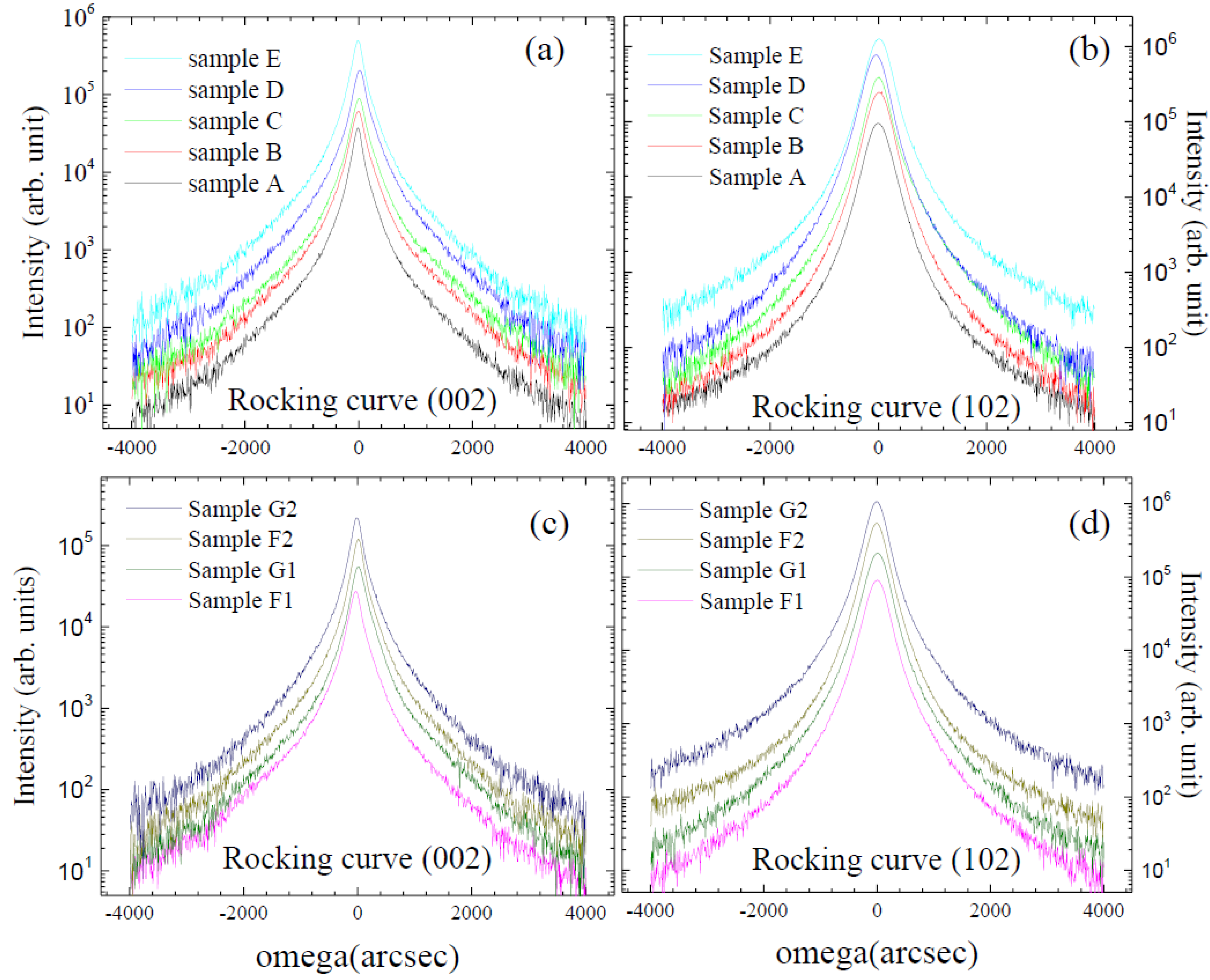
Figure 5.
FWHM of rocking curves for (002) and (102) directions versus N/Ga flux ratio for Series 1. The inset shows the bar chart for the FWHM of samples in Series 2.
Figure 5.
FWHM of rocking curves for (002) and (102) directions versus N/Ga flux ratio for Series 1. The inset shows the bar chart for the FWHM of samples in Series 2.
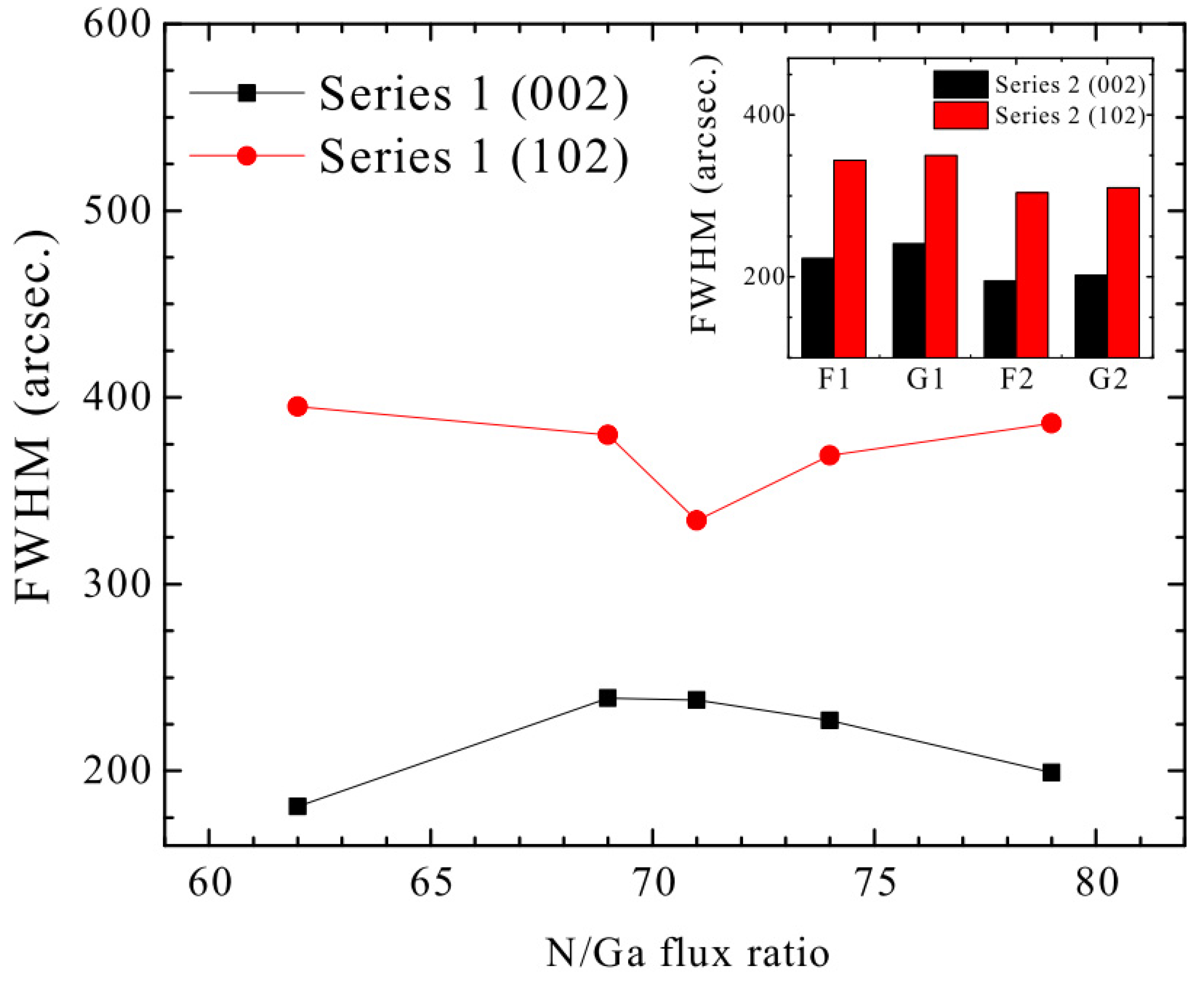
Figure 6.
Ramen spectra of different skin depths of the samples: (a) including bottom substrate and (b) near the surface. The y-axis has been offset for comparison.
Figure 6.
Ramen spectra of different skin depths of the samples: (a) including bottom substrate and (b) near the surface. The y-axis has been offset for comparison.


Table 1.
Growth parameters of Mg-doped GaN, where N/A stands for “Not Applicable”.
| Sample | Ga Flux (×10−7 Torr) | Flux Ratio (N/Ga) | Modulated Shutters | Shuttering Period (Open/Close) |
|---|---|---|---|---|
| A | 1.45 | 62 | none | N/A |
| B | 1.30 | 69 | none | N/A |
| C | 1.25 | 71 | none | N/A |
| D | 1.20 | 74 | none | N/A |
| E | 1.15 | 79 | none | N/A |
| F1 | 1.80 | 50 | Mg, Ga | 10 s/10 s |
| G1 | 1.60 | 56 | Mg, Ga | 10 s/10 s |
| F2 | 1.80 | 50 | Ga | 10 s/10 s |
| G2 | 1.60 | 56 | Ga | 10 s/10 s |
Table 2.
Hall measurement results.
| Sample | Type | Carrier Concentration (cm−3) | Mobility (cm2/Vs) | Resistivity (Ω-cm) |
|---|---|---|---|---|
| A | n | 6.84 × 10¹⁸ | 104.48 | 8.74 × 10⁻³ |
| B | n | 1.61 × 10¹⁸ | 124.92 | 3.10 × 10⁻² |
| C | p | 2.15 × 10¹⁵ | 31.08 | 9.36 × 101 |
| D | p | 3.59 × 10¹⁷ | 4.39 | 3.61 × 100 |
| E | p | 3.12 × 10¹⁸ | 0.97 | 2.06 × 100 |
| F1 | p | 2.70 × 10¹⁷ | 4.90 | 4.37 × 100 |
| G1 | p | 1.79 × 10¹⁶ | 9.81 | 3.55 × 101 |
| F2 | p | 1.42 × 10¹⁷ | 30.16 | 1.45 × 100 |
| G2 | p | 3.92 × 10¹⁶ | 24.90 | 6.41 × 100 |
Table 3.
FWHM of XRD rocking curve (arcsec.).
| Sample | A | B | C | D | E | F1 | G1 | F2 | G2 |
|---|---|---|---|---|---|---|---|---|---|
| (002) | 181 | 239 | 238 | 227 | 199 | 223 | 241 | 195 | 202 |
| (102) | 395 | 380 | 334 | 369 | 386 | 344 | 350 | 304 | 310 |
Disclaimer/Publisher’s Note: The statements, opinions and data contained in all publications are solely those of the individual author(s) and contributor(s) and not of MDPI and/or the editor(s). MDPI and/or the editor(s) disclaim responsibility for any injury to people or property resulting from any ideas, methods, instructions or products referred to in the content. |
© 2023 by the authors. Licensee MDPI, Basel, Switzerland. This article is an open access article distributed under the terms and conditions of the Creative Commons Attribution (CC BY) license (https://creativecommons.org/licenses/by/4.0/).
Share and Cite
MDPI and ACS Style
Wang, Y.-C.; Lo, I.; Lin, Y.-C.; Tsai, C.-D.; Chang, T.-C. Improvement of Mg-Doped GaN with Shutter-Controlled Process in Plasma-Assisted Molecular Beam Epitaxy. Crystals 2023, 13, 907. https://doi.org/10.3390/cryst13060907
AMA Style
Wang Y-C, Lo I, Lin Y-C, Tsai C-D, Chang T-C. Improvement of Mg-Doped GaN with Shutter-Controlled Process in Plasma-Assisted Molecular Beam Epitaxy. Crystals. 2023; 13(6):907. https://doi.org/10.3390/cryst13060907
Chicago/Turabian StyleWang, Ying-Chieh, Ikai Lo, Yu-Chung Lin, Cheng-Da Tsai, and Ting-Chang Chang. 2023. "Improvement of Mg-Doped GaN with Shutter-Controlled Process in Plasma-Assisted Molecular Beam Epitaxy" Crystals 13, no. 6: 907. https://doi.org/10.3390/cryst13060907
Note that from the first issue of 2016, this journal uses article numbers instead of page numbers. See further details here.