


Research Progress and Development Prospects of Enhanced GaN HEMTs

Laser Institute, Qilu University of Technology (Shandong Academy of Sciences), Jinan 250104, China
*
Author to whom correspondence should be addressed.
Crystals 2023, 13(6), 911; https://doi.org/10.3390/cryst13060911
Submission received: 15 April 2023
/
Revised: 15 May 2023
/
Accepted: 26 May 2023
/
Published: 4 June 2023
(This article belongs to the Special Issue III-Nitride Materials: Properties, Growth, and Applications)
Abstract
:With the development of energy efficiency technologies such as 5G communication and electric vehicles, Si-based GaN microelectronics has entered a stage of rapid industrialization. As a new generation of microwave and millimeter wave devices, High Electron Mobility Transistors (HEMTs) show great advantages in frequency, gain, and noise performance. With the continuous advancement of material growth technology, the epitaxial growth of semiconductor heterojunction can accurately control doping level, material thickness, and alloy composition. Consequently, HEMTs have been greatly improved from material structure to device structure. Device performance has also been significantly improved. In this paper, we briefly describe MOCVD growth technology and research progress of GaN HEMT epitaxial films, examine and compare the “state of the art” of enhanced HEMT devices, analyze the reliability and CMOS compatibility of GaN devices, and look to the future directions of possible development.
1. Introduction
With the rapid advancement of information and communication technologies continuing to change us and the world we live in, communication equipment and other electronic devices must be developed for high-speed, high-frequency, digital circuits, and microwave circuits with low-noise applications. At present, the development of wide bandgap semiconductor materials, such as gallium nitride (GaN) and silicon carbide (SiC), are relatively mature. Thanks to the high saturated electron drift speed, high breakdown electric field, radiation resistance and other excellent physical properties, GaN and SiC are ideal for microwave electronic devices and are widely used in the field of wireless base stations, satellite TV, and radar [1,2]. SiC has a clear advantage in high voltage (higher than 1200 V) applications, while GaN prevails in power conversion and high-frequency work. In particular, GaN-based HEMTs, which generate a high concentration of two-dimensional electron gas (2DEG) at the heterostructural interface and have on resistance 30% to 50% lower than SiC devices [3,4], are ideal for the next generation of high-frequency, high-power power electronics applications. It can be widely used in all kinds of electronic products, new energy vehicles, industrial applications, 5G communication and other important fields.
After nearly 30 years of development, the performance of GaN-based HEMTs continues to improve. SiC substrate is of high price while GaN-based HEMTs on Si substrate can achieve large-scale industrialization at low cost due to the mature development of Si semiconductor technology, which is easy to back-end process compatibility and has been widely used in consumer electronics and on-board electronics markets. Conventional GaN HEMTs are depletion types in which the device gate still has a high concentration of 2DEG in the channel at zero bias, leaving the device on. The enhanced GaN HEMT is safer and more energy efficient because it exhausts the 2DEG in the channel at zero grid bias, and the device is in the off state. Therefore, GaN-enhanced HEMT devices have important strategic research significance. This paper mainly introduces the growth technology of GaN HEMT epitaxial thin film, summarizes and compares the international mainstream enhanced HEMT device structure and preparation process, analyzes the existing problems and solutions of material epitaxial, device structure and preparation process, and puts forward the future possible development scheme.
2. Growth Technology and Progress of GaN HEMT Epitaxial Films
With the emergence of the wide bandgap semiconductor materials, GaN-based semiconductor materials and their multi-component alloy compounds showed excellent optical, electrical, chemical, physical and other properties, which has become the main focus of research in semiconductor materials and devices [5,6,7] since the end of the 20th century. Due to the limitation of the GaN substrate, group III nitrides are generally grown by heteroepitaxy. There are three substrates commonly used at present, which are sapphire, SiC, and Si. GaN-based heterostructures were prepared on a sapphire substrate for the first time in 1992. AlGaN/GaN heterostructures can induce two-dimensional electron gas with high surface density and high electron mobility without intentional doping, thanks to the spontaneous and strain-induced polarization [8,9], and related power devices have been widely studied. HEMT devices have gradually become the focus of research due to their advantages in high temperature, high power, high frequency, high radiation and other fields.
2.1. GaN HEMT Based on Single Heterojunction
The performance of HMET devices is mainly determined by the electrical properties of 2DEG. Electron concentration and corresponding electron mobility are the two main indices used to measure the electrical properties of 2DEG. With the continuous improvement of the performance of AlGaN/GaN heterojunction, the low-temperature mobility also increases [10,11,12]. Because the lattice mismatch and thermal mismatch between SiC and GaN are smaller than that of sapphire, the GaN HEMTs on SiC have better epitaxial growth quality and performance. However, at the same time, it is found that SiC substrate is expensive and extremely difficult to grow, not conducive to industrialization. Although Si substrate has a large lattice mismatch with GaN, it is the cheapest and easiest to prepare into substrate wafers of different sizes (2–12 inches). In addition, silicon-based GaN devices can be integrated with traditional silicon-based devices on the same wafer to achieve system-level integration. Therefore, the research of GaN HEMTs on Si substrate has received more attention in recent years.
The core of GaN-based HEMT materials consists of semi-insulated GaN (base layer) and AlGaN (barrier layer), and the growth of the GaN base layer is the basis for the growth of the entire GaN-based HEMT material. Therefore, the growth of high-quality GaN materials is a prerequisite for the research and development of GaN-based devices. At present, epitaxy techniques for GaN thin films mainly include metalorganic chemical vapor deposition (MOCVD), molecular beam epitaxy (MBE), and hydride vapor phase epitaxy (HVPE). Among them, the epitaxial layer grown by metalorganic chemical vapor deposition technology has the advantages of low surface roughness, high purity, and easy mass production.
The biggest challenge in the growth of GaN-based HEMTs is how to epitaxy the well-insulated GaN buffer layer on a suitable substrate. First, the polarization and defects of GaN itself lead to the high electron concentration of intrinsic GaN. Meanwhile, the lattice mismatch (17%) and thermal mismatch (56%) between GaN and Si substrate lead to the cracking and warping of GaN film [13], resulting in many dislocations and defects and the remelting corrosion of Ga atoms and Si substrate [14]. In recent decades, researchers have completed a number of studies to improve the crystal quality of GaN films: for example, the low-temperature buffer layer and superlattice technology [15,16,17]. In 2005, Cordier et al. [18] grew AlGaN/GaN HEMTs epitaxial on Si substrate with AlGaN buffer layer technology, and the two-dimensional electron gas concentration of 5 × 1012 cm−2 and mobility of 1400 cm2/Vs. In 2013, Chen et al. studied the growth of high-resistance GaN structures [19] and found that the active carbon mixing technology using active C3H8 gas as a carbon source could improve the carbon mixing concentration of GaN and the resistivity of high-resistance GaN structures, thus enhancing the voltage resistance performance of Si-based GaN HEMTs. In 2017, the world’s first eight-inch silicon-based gallium nitride mass production line of Zhuhai Innoseco was put into operation, which means that Chinese domestic enterprises have entered the forefront of the world in GaN semiconductor competition. The eight-inch silicon-based gallium nitride epitaxial technology produced by the company has successfully broken through the global difficulties of wafer manufacturing, such as low warpage, low defect and dislocation density, and low leakage current, and has been widely used [20].
With the development of epitaxial GaN technology on Si substrates, the epitaxial crystal quality of GaN HEMT devices is increasing more and more. In 2000, Kaiser et al. [21,22] first proposed AlGaN/GaN heterojunction HEMTs on Si(111) substrate. In 2020, Pandey et al. adopted a stepped GaN buffer layer to adjust AlGaN/GaN structure [6] to improve its structure and 2DEG characteristics. However, tests showed that its composite dislocation density was in the order of 109 cm−2, and its density of 2DEG was in the order of 6.92 × 1012 cm−2, which was still not ideal.
At present, by adjusting and optimizing the AlGaN/GaN superlattice stress control layer, a six-inch GaN HEMT epitaxial film on a silicon substrate has been obtained with good performance in warpage control, crack level, crystal quality, and surface morphology. Its structure is shown in Figure 1 [23]. In 2021, Bose et al. [24] reported the 3C-SiC/Si-based AlGaN/GaN HEMT with a stable temperature. High-quality AlGaN/GaN heterostructures were achieved by MOCVD on a six-inch Czochralac single-crystal Si substrate without cracks. However, it is still a great challenge for AlGaN/GaN structures to reduce the dislocation density of the GaN buffer layer and increase the density of 2DEG. Therefore, further research is needed for AlGaN/GaN heterogeneous structures.
2.2. GaN HEMT Based on Double-Heterostructure
In recent years, GaN-based HEMTs have received extensive attention and research. In particular, AlGaN/GaN HEMTs have achieved rapid development in material quality and device performance, and great progress has been made in microwave characteristics. However, for K-band high-frequency devices, the gate length (LG) of the transistor needs to be less than 0.4 μm. For conventional AlGaN/GaN single-heterostructure HEMT devices, when the gate length decreases, the 2DEG limit in the well becomes worse. At high leakage voltage or gate voltage, electrons are easy to overflow into the buffer layer, resulting in buffer layer leakage, which seriously affects the peak current, resulting in large threshold voltage drift, soft turn-off phenomenon, high threshold current and other problems. At the same time, serious current collapse [25], large leakage current [26,27] and high-temperature thermal stability and other reliability problems have always existed. Double-heterostructure involves inserting a back barrier between the GaN channel layer and buffer layer to prevent electrons from flowing to the buffer layer so that 2DEG can be better confined in a quantum well. The advantages of double-heterostructure can be used to better solve these problems, which are widely used in millimeter waves.
There are two kinds of back barriers commonly seen in GaN base heterostructures before. One is to replace the GaN buffer layer with an AlGaN layer. The other is to insert AlGaN or InGaN layer under the channel layer, and the buffer layer remains unchanged. In 1997, heterostructure devices were first reported. Fan et al. developed AlGaN/GaN/AlGaN/GaN double-heterostructure field-effect transistor, which still has large transconductance at 573 K high temperature. It is proved that the grid has a good ability to regulate the channel current, and it also reflects the importance of the back-barrier structure to improve the 2DEG domain [28]. In 2011, Lee et al. made HEMT devices using the InAlN/GaN/AlGaN double-heterostructure material formed by the AlGaN buffer layer as the back barrier. The short channel effect in the components is significantly suppressed, and the high-frequency energy ratio is effectively improved [29]. In 2013, FaridMedjdoub et al. used MOCVD to grow AlN/GaN/AlGaN double-heterostructure [30], which achieved a breakdown voltage of more than 100 V and a power gain of more than 200 GHz on a Si substrate. In 2018, Chang Gung University in Taiwan reported an enhanced high electron mobility transistor device with a gradient barrier layer [31]. It was found that using a gradient barrier can reduce the off-state leakage current by one order of magnitude, which can effectively improve the uniformity of threshold voltage.
With the advancement of science and technology, higher requirements are put forward for performance, which requires further reduction of the grid length of components. The advantages of double-heterostructure in the application of high power and high frequency are becoming more and more obvious. Double-heterostructure can use the optimized process and structure of single-heterostructure, but because of the addition of an extra barrier, the strain of heterostructure materials will change. The region limit of 2DEG is greatly improved, which also puts forward more strict requirements on the interface roughness. At the same time, due to the large mismatch problem of GaN HEMTs on Si substrates, the epitaxy and process complexity of GaN-based double-heterostructure materials are more challenging. Therefore, it is of great significance to study the characteristics of GaN-based double-heterostructure materials and their devices.
3. Enhanced GaN HEMT Devices
SiC-based GaN HEMTs have been successfully used in the UHF ~ W band. However, SiC substrate materials are costly and difficult to further monolithic integration with Si or GaAs material systems into complex multifunctional ICs. To further reduce the cost of GaN HEMTs, Si-backed GaN HEMTs have been developed. In the last two years, Si-based GaN HEMTs have been moving toward engineering direction, with continuous innovation in new device structure, CMOS process compatibility and reliability, and will be competitive with SiC-based RF GaN HEMTs in low-cost and mass-production applications in the future.
In many applications of power semiconductor devices, enhanced transistors with positive threshold voltage will bring great convenience in applications. When the grid driver circuit of the power device fails, the conduction channel of the enhanced power device will be shut off below the grid region, which will not cause an irreparable impact on the system. For depletion devices, when the gate drive fails, a conducting channel below the gate of the device is always present, which may cause unwanted current paths to occur and result in irreparable damage to the system. In the field of microwave/RF power amplification devices, enhanced power semiconductor devices enable a single power supply, further reducing the area of the chip and system. At present, the enhanced technologies for GaN-on-Si power devices are as follows: concave-gate, fluorinated gate, p-GaN intercalation layer, common-source common-gate cascade (cascode) and barrier thinning technique. In this paper, we review the technical principles of enhanced GaN HEMTs and their advantages and disadvantages. We also examine the latest research progress of enhanced GaN HEMTs and the latest GaN device solutions in the industry. We then discuss the development direction of enhanced GaN HEMTs in the future.
3.1. Concave-Grid Structure
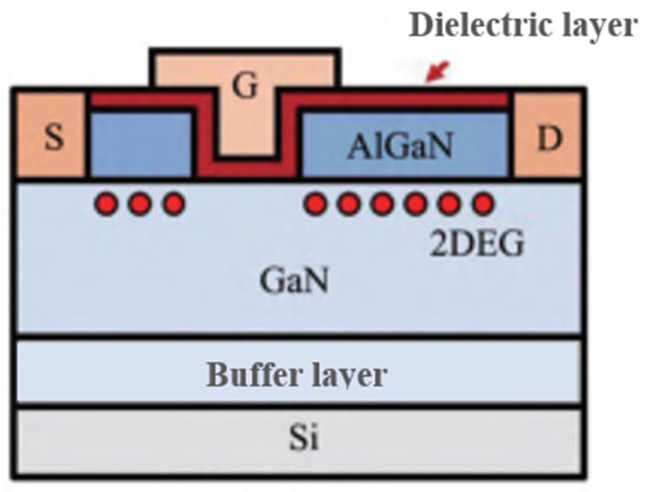
The concave gate structure achieves enhanced HEMT devices by partially or completely etching the barrier layer at the AlGaN/GaN heterojunction, reducing the polarization effect of the heterojunction and decreasing the distance between the gate metal and the channel. Combined with the electric field generated by Schottky contact, the 2DEG induced under the grid is exhausted together so that the channel is clipped when the grid voltage is 0 V. Figure 2 shows the structure diagram of the concave gate structure to realize the enhanced Gan-based device [3]. The advantage of this structure is that the grid drive circuit is relatively simple, and the grid voltage tolerance of the device can be adjusted by adjusting the thickness of the grid dielectric layer, which not only improves the grid control ability of the device but also greatly improves the frequency and transconductance of the enhanced device.
In 2003, Okita et al. [32] successfully prepared enhanced AlGaN/GaN MIS-HEMT devices using a concave gate structure. However, concave gate etching is easy to introduce etching damage and interface states, which seriously affects the performance reliability of such devices and limits their commercial development. To solve this problem, researchers at home and abroad have put forward a number of solutions. In 2010, Burnham S D et al. proposed a low-damage “digital etching technology”, which has high etching accuracy, good etching morphology at the interface formed by the grid, and the prepared transverse enhanced GaN HEMTs with a breakdown voltage of up to 1100 V [33]. The technology of concave gate etching combined with a secondary epitaxial AlGaN barrier layer was proposed by Fukui University in Japan. A new semiconductor-insulator interface is formed through secondary epitaxy, which greatly reduces the influence of dry etching on the density and mobility of 2DEG. The threshold voltage of devices using this scheme is as high as 2.3 V, and the saturation current is as high as 425 mA/mm, which has great potential [34]. Im et al. studied the corrosion technology scheme of tetramethylammonium hydroxide and obtained the device threshold voltage up to 3.5 V [35]. To date, relevant research has been ongoing.
Generally, an insulating dielectric layer will be grown between the gate metal and the AlGaN barrier layer for concave gate structure devices to suppress the gate leakage current generated during the device’s working process and further improve the gate threshold voltage of the device. However, the charge and defect of dielectric layer/semiconductor interface will lead to the poor stability of the device threshold voltage. Therefore, in the pursuit of high-performance GaN HEMTs, the interface state of the gate slot and the quality of the dielectric layer are important indicators.
3.2. Fluorinated Grid Structure
The enhanced HEMTs based on the fluorinated grid structure are realized by using a fluoride ion implantation technique that injects a dose of fluoride ions into the barrier layer of the grid. The fluorine ions entering the AlGaN barrier layer will form a negatively charged fixed charge, resulting in a higher barrier height of the barrier layer, thus increasing the conduction band energy level at the heterojunction interface. When the bottom of the conduction band level exceeds the Fermi level, the 2DEG in the channel under the grid is exhausted, and the threshold voltage is shifted forward. Figure 3 shows the structure of an enhanced GaN HEMT with a fluorinated gate structure [3]. Enhanced GaN HEMTs based on fluorine injection technology provide high forward threshold gate voltages, good suppression of gate leakage current, and improved gate swing. However, the disadvantage is that a large number of empty and interfacial states will be formed by ion implantation, which reduces the stability of threshold voltage [36].
Researchers have engaged in a substantial amount of effort to solve the gate damage caused by fluoride ion implantation. In 2015, Zhang et al. used LPCVD-SiN as the grid dielectric layer and energy absorption layer to reduce grid damage, with a threshold voltage of 3.3 V and saturation current of 200 mA/mm [37]. In 2018, Ling et al. [38] prepared an enhanced GaN HEMT device by depositing the TiN side wall and TiN layer in contact with the source electrode and using a two-step fluoride treatment technology. The two-step fluoride treatment technology increases the height of the back-barrier, reduces the gate leakage current, and effectively reduces the source resistance. When the TiN layer thickness is 1 μm, the maximum leakage current reaches 845 mA/mm, and the peak transconductance (412 mS/mm) is 21.2% higher than that of the conventional device (340 mS/mm). In 2020, Zheng et al. [39] studied the physical mechanism of HEMT threshold voltage degradation of fluoride ion structure and found that due to the existence of the reverse gate stress, the higher the density of electrons injected under the gate, the more intense the collision ionization with fluoride ions, and the more serious the threshold voltage degradation. However, after a certain period of annealing, the electrons in the channel will tunnel into the neutral trap generated by the gate stress in the barrier layer and be captured, which inhibits the degradation of the threshold voltage. This study provides a reference for further realization of high-performance GaN devices by fluoride treatment.
3.3. p-GaN Grid Technology
The p-GaN grid technology is the most representative method for the implementation of enhanced GaN HEMTs. This technology was first proposed by Uemoto et al. in 2007 [40], with advantages such as simple process, good compatibility, and strong scalability. At present, it is the only technical solution that has realized large-scale production. An enhanced HEMT based on p-GaN gate technology is constructed by depositing a p-GaN cap layer above the AlGaN barrier layer and sputtering a metal gate layer on top. The doping concentration and thickness of p-GaN are closely related to the on-resistance and threshold voltage of the device. Figure 4a shows the structure of an enhanced GaN HEMT using p-GaN gate technology [3].
The energy band changes at the heterojunction before and after the p-GaN cap layer are shown in Figure 4b [41]. When the p-GaN cap layer is introduced, the conduction band level at the AlGaN/GaN heterojunction interface will cross the Fermi level at zero bias so that the 2DEG at the heterojunction interface will be exhausted, resulting in the effective channel clamping under the gate. When a forward bias is applied, the HEMT device is turned on as the 2DEG under the grid recovers. The enhanced device achieved by this technology has stable threshold voltage, low on-resistance, and strong reliability. However, due to the epitaxial layer crystal quality and p GaN etching damage and other problems, the breakdown voltage is generally low, which seriously restricts its development in new energy vehicles, photovoltaic, and other high voltage fields.
In terms of device structure design, the vertical or quasi-vertical structure can effectively improve the breakdown voltage of GaN devices. The breakdown voltage of GaN power-switching devices with vertical structures has been reported to be as high as 1200 V [42]. However, the vertical structure is difficult to realize the single-chip preparation of capacitors, resistors, diodes, and enhanced/depleted GaN devices, which is not conducive to the development of GaN single-chip integration technology. In contrast, the horizontal structure based on AlGaN/GaN heterojunction is easier to realize monolithic integration, which can further promote the development of intelligent, lightweight and miniaturized power systems. In addition, GaN devices with p-GaN gate structures still have many problems, such as gate leakage, poor reliability, small grid voltage swing and so on [43]. Therefore, how to increase the breakdown voltage and improve the grid operating stability of the device is very important for the development of high-performance, high-voltage GaN HEMTs.
In recent years, it has been found that the doping concentration of the p-GaN layer needs to exceed 1018 cm−3 to effectively deplete the grid region. In addition, it is reported that it is easier to obtain higher threshold voltage and lower gate-drain current by using the Schottky junction. Postuma et al. reported that the threshold voltage of a device gate electrode made of TiN could reach 2.1 V [44]. Lukens et al. reported a “first gate” self-aligning process using Mo as both the etched mask layer and the gate metal and found that the barrier degradation of the device did not occur after high-temperature annealing [45]. In view of the generally low breakdown voltage of p-GaN grid HEMTs, domestic and foreign researchers have continuously optimized and innovated the process or structure in recent years [46,47,48]. At present, the breakdown voltage is mainly improved by designing various field plate structures. In 2020, Hu et al. [49] proposed the dual-field plate combination structure technology of source field plate and grid field plate, which achieved uniform distribution of electric field and a breakdown voltage of up to 600 V. At the same time, NH3 plasma treatment significantly reduced the dynamic on-resistance of the device, with a threshold voltage of 3.7 V and a saturation current of 132 mA/mm. In order to achieve a good performance compromise between breakdown voltage and on-resistance of the device, Wei et al. [50] manufactured a transverse-coupled p-GaN gate HEMT device in 2021, which uses hydrogen plasma to treat p-GaN. The device structure is shown in Figure 5. When the width and spacing of the p-GaN strips are small enough, the coupling effect in the depletion region enables a good compromise between the breakdown voltage and the on-resistance of the device. When the spacing between the p-GaN and drain is 10 μm, the device performance is optimal, the on-resistance is as low as 11.54 Ω·mm, and the breakdown voltage can reach 880 V.
Surface passivation technology is very important for GaN HEMTs to solve leakage and reliability problems. On the one hand, using high-quality SiNx, Al2O3 and other media for surface passivation [51] can reduce the transition leakage generated by surface defects and improve the breakdown voltage of the device. On the other hand, because the AlGaN barrier layer is very thin, a high-quality medium can effectively passivate the surface of GaN devices, reduce the current collapse effect caused by surface and interface states, and improve the operating stability of the devices [52].
3.4. Common Source and Common Gate Cascade (Cascode) Structure
Cascode cascade architecture is an important technical route for enhanced GaN HEMTs. As a transition technology from Si-based power devices to pure GaN-based power devices, it adopts a common source and common gate connection with Si-based MOSFETs and depletion-type GaN HEMTs, and its equivalent circuit structure is shown in Figure 6. The drain D of the Si-based transistor is connected to the source S of the GaN HEMT, and the gate G of the GaN HEMT is connected to the source S of the Si-based transistor. At the same time, the gate threshold voltage of the Si-based MOSFET is used as the threshold voltage of the entire device, which controls the on-off and on-off of the entire cascode device.
The advantages and disadvantages of the enhanced device realized by cascode cascade technology are obvious. The advantage is that it bypasses the technical difficulties of enhanced HEMTs, provides a high threshold voltage and stability, matches well with existing Si circuits, and provides a simple drive circuit. Cascode technology is, therefore, ideal for large-scale applications. In 2012, Transphorm in the United States introduced the commercially enhanced cascode GaN transistor, followed by Fujitsu in Japan, Anson in the United States, and other semiconductor giants led by Transphorm in the United States have introduced enhanced GaN transistors using cascode cascade technology. Cascode cascade technology is one of the GaN enhancements that have been successfully commercialized. The disadvantage is that Si-based transistors have low electron mobility and poor high-frequency response. At the same time, the cascode cascade has capacitor mismatch problems and is far less capable of high-temperature resistance and miniaturization than non-cascaded enhanced GaN HEMTs, limiting its future application.
In order to improve the effect of Si material on the overall performance of devices, many attempts have been made. The Hong Kong University of Science and Technology has studied the cascade structure based on the combination of SiC transistor and GaN-based HEMT, which significantly increases the breakdown voltage of the device up to 1200 V and has lower switching loss, which has great development space [53]. To reduce the parasitic effect of cascade technology, Zhang et al. [54] proposed transfer printing and self-aligned etching technology in 2020. The enhanced cascode FET device integrated into a single piece effectively solves the parasitic effect and has good threshold voltage uniformity (2.0–2.2 V). At the same time, the grid voltage swing reaches ±18 V, and the grid leakage current is lower than 10−5 mA/mm.
In summary, it can be found that the related performance of each enhanced device has been continuously improved, and some disadvantages have been effectively solved. However, in practical applications, in addition to considering good performance and reliability of devices, they should also be well suited to circuit topology, layout interconnection and package design. Therefore, in future studies, further optimization of the device structure, improvement of process design level, improvement of device reliability and continuous promotion of product design of various enhanced devices are important directions.
3.5. Barrier Thinning Technique
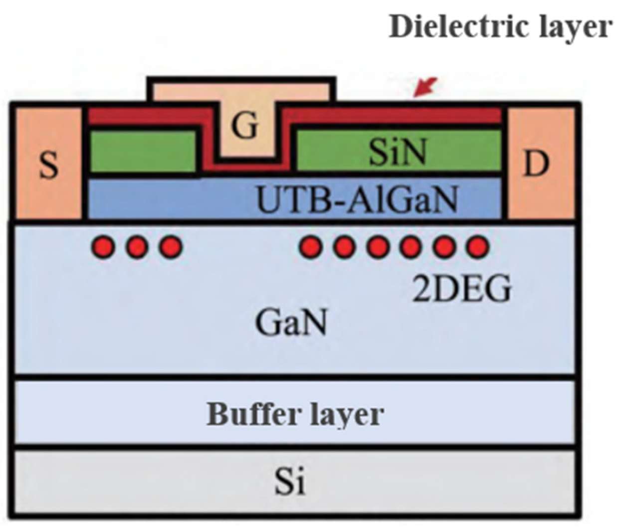
The thinning barrier technique first evolved from the concave grid structure, and its structure is shown in Figure 7. By reducing the thickness of the AlGaN barrier layer, the polarization charge density of the barrier layer is reduced. When it is reduced to a certain value, the channel will not generate 2DEG induction. From the perspective of energy band structure, with the thinning of the barrier, the conduction band at AlGaN/GaN heterojunction rises. When it rises above the Fermi level, the existing two-dimensional potential well disappears, thus depleting 2DEG and achieving the preparation of enhanced devices. The thin barrier AlGaN/GaN heterojunction has lower polarization charge density and 2D electron gas density than conventional AlGaN/GaN heterojunction, so the thin barrier AlGaN/GaN heterojunction is suitable for enhanced HEMT devices. With the thinning barrier technique, the AlGaN barrier layer with a thickness of less than 5 nm is naturally grown on the GaN layer instead of etching the AlGaN barrier layer [55,56,57], which further simplifies the process. Because the concave gate etching damage is avoided, there is no high-density interface state trap under the gate of GaN-enhanced devices prepared by using ultra-thin barrier technology. The threshold voltage is stable, and the preparation consistency is good. However, the decrease of 2DEG density can also cause adverse problems such as higher on-resistance and lower breakdown voltage of HEMTs. To make the thin barrier AlGaN/GaN heterojunction with enhanced work and good on-resistance and breakdown voltage, researchers at home and abroad have carried out research on the material structure, technology, and enhanced devices.
In 2019, Han et al. [58] prepared an ultra-thin barrier-enhanced MIS-HEMT device by using SiN as the passivation layer, AlOX as the dielectric gate layer and a ferroelectric charge trap gate stack. Compared with the traditional hollow gate-enhanced GaN HEMT device, the device not only guarantees higher threshold voltage and maximum leakage current but also has better threshold voltage stability, with a threshold voltage of 3.19 V and a maximum leakage current of 716 mA/mm. An enhanced GaN HEMT device with an AlGaN barrier layer of only 4 nm was reported by the Institute of Microelectronics, where a layer of Si3N4 film was grown above the channel layer in the non-gate region, restoring 2DEG concentration. The exposed AlGaN barrier layer above the gate region is treated by in-situ RPP technology of plasma-enhanced atomic layer deposition (PEALD), and then a layer of Si3N4 gate dielectric layer is grown. The final prepared device has good threshold voltage stability and a maximum output current [59]. Therefore, it can be found that the recovery effect of the SiNX passivation layer on 2DEG concentration in the non-gate area solves the problem of large on-off resistance of AlGaN/GaN HEMTs with a thin barrier, and the thin barrier technology has great research potential to realize enhanced AlGaN/GaN HEMTs.
In conclusion, we found that the initial HEMT devices, which used Schottky grids directly, had high grid leakage and small grid voltage swings, which made the grid easily break down and ultimately lose reliability. In addition, a large number of donor-like defects exist on the AlGaN surface due to suspension keys and other factors, leading to the current collapse effect of AlGaN/GaN HEMTs in RF applications. Growing a dielectric layer on top of the AlGaN barrier or GaN channel layer to form a metal-insulator-semiconductor (MIS) structure is a powerful solution and has been extensively studied.
3.6. GaN MIS-HEMT Devices
MIS-HEMT device architecture is one in which an insulating layer is inserted between a metal gate and a semiconductor layer. As shown in Figure 8, compared with metal-semiconductor contact, the MIS-HEMT insulator layer as a passivation layer can passivate defects and suspension keys on the material surface, reduce leakage on the device surface, reduce current collapse effect, and thus increase the breakdown voltage of the device. As the grid dielectric layer, it can effectively reduce grid leakage, improve the grid voltage swing, and enhance the reliability and stability of the grid.
In MIS structure, the selection of a grid dielectric layer is very important. On the one hand, the larger the dielectric constant, the larger the transconductance of MIS-HEMT devices. On the other hand, the larger the bandgap width of the medium, the smaller the gate leakage of the device [61]. Therefore, GaN MIS-HEMT devices usually use the gate media with a higher dielectric constant, wider bandgap, and higher MIS interface quality. The high-K gate dielectric with a dielectric constant K greater than 3.9 is the mainstream dielectric material for MIS-HEMT devices, which has the advantages of a high protective output current, large transconductance movement, small gate leakage and inhibition of the short channel effect. At present, the mainstream materials of gate media are SiNX, Al2O3, HfO2, etc. [62,63]. In addition, considering the cost, mass production and subsequent process compatibility, most GaN MIS-HEMT devices in the market are based on GaN-on-Si materials.
During the fabrication of GaN MIS-HEMTs based on Si, the growth quality and process compatibility of dielectric films are the key elements that determine the device’s characteristics. Different types of the dielectric layer and dielectric layer growth quality directly determine the positive compressive strength of the grid and then affect the final output current density of the device. The growth mode of dielectric films can be divided into two types: ex-situ growth and in-situ growth. In-situ growth avoids the problems of in-situ oxidation and surface pollution, and the quality of the dielectric film and interface is better, so it has become a hot topic in the research of dielectric growth. However, the type of medium grown by the in-situ growth method is limited, generally silicon nitride (SiNx) medium. The SiNx medium grown in situ by MOCVD is generally thin (less than 10 nm) due to stress release and other problems. With the increase in thickness, the quality of the SiNx medium will deteriorate and even crack. Therefore, in-situ growth of the high-quality SiNx dielectric layer and the related performance characterization have been both the focus and difficulty of this research. In 2014, P. Meons et al. prepared AlGaN/GaN depletion MIS-HEMT devices with a breakdown voltage of 650 V by in-situ growth of SiNx as a gate medium [64]. In 2021, Nanjing University studied the preparation of depletion-type AlGaN/GaN MIS-HEMT devices on Si substrate, using MOCVD to grow SiNx dielectric layer (about 47 nm) in situ [65]. The saturation output current of the device is 603 mA/mm, and the off-state breakdown voltage reaches 1348 V. It will be a future trend to put Si-based GaN MIS HEMTs with high -K gate media into the market for industrialization.
4. The Reliability of GaN HEMT Devices
The reliability problem of power devices must be solved from product to application. At present, many studies on the reliability of GaN-enhanced power devices have been reported, such as high-temperature reverse bias, high-temperature gate bias stress, short circuit safety working area, etc. [66,67,68]. Gan-based HEMTs are popular because of their huge advantages in millimeter wave and radio frequency fields. For example, GaN processes for 5G FR2 must achieve gate length ≤0.15 μm to provide effective performance [69]. At the same time, they must be economically viable in low-cost communications applications. In this sense, while silicon carbide (SiC) substrates offer the most advanced monolithic microwave integrated circuit (MMIC) design performance, a new generation of GaN-on-Si RF devices is being developed that can reduce substrate costs and utilize existing silicon-based RF and digital processing technologies [70,71,72]. Because the Si substrate’s heat dissipation performance is worse than SiC, the long-term reliability of GaN-on-Si HEMTs in practical applications needs to be fully investigated.
The material properties and the manufacturing process of the device will inevitably introduce various defects and eventually form an electronic trap. These electronic traps can damage the performance and stability of the device while also causing the device to have complex electrical characteristics, such as delayed response, self-heating effect, current collapse, etc. The trap center of the device is generally distributed in the device surface, barrier layer, and buffer layer. Different device manufacturing and growth methods lead to different trap mechanisms.
Current collapse refers to the phenomenon that the output current swing decreases sharply under the drive of high frequency and large signal, resulting in the decrease of output power density and additional power efficiency. The main reason is that the hot electrons in the channel are captured by the deep-level trap in the buffer layer under the action of a strong field, which leads to a sharp decrease in the current in the channel. This pass is recoverable, and when the strong field is removed, or the appropriate light is added, the current can also be gradually restored. This effect is very important for the test and characterization of the device. The delay response includes gate delay and leakage delay. The gate delay is mainly caused by the surface state of the device, and the leakage delay is mainly caused by the deep-level trap in the buffer layer. When the device is applied at high voltage and high current, the heat generated at the channel will make the lattice temperature rise significantly and then cause the effect of device characteristic degradation, which is called the self-heating effect. The existence of trap charge and the low heat dissipation rate of Si substrate further aggravate the self-heating effect. Due to the presence of self-heating and trap charges, the DC and RF characteristics of the device are reduced, resulting in serious degradation of the device’s output power, transconductance, cut-off frequency, and reliability. Therefore, accurate testing of trap effects on GaN HEMTs is necessary to achieve both design objectives and reliability predictions [73]. The physical mechanism of the trap effect is complex. Different trap centers are distributed in different positions of the device, and the constant number between the capture and firing time of each trap energy level may be different, which brings great challenges to the test and characterization of devices.
Pulse IV(PIV) test is a common way to characterize trap effects. By designing pulse width, these trap effects can be characterized separately. However, the test results are strongly dependent on the setting of the time constant and pulse test time associated with the trap. However, fast charge capture times (down to the ns-range) combined with slow charge release (in the ms-range and above) cause each point on the PIV to belong to a different trapping state [74], preventing the acquisition of reliable datasets for GaN device modeling. Although specific multi-pulse techniques for trap-state conditioning [75,76] based on tailored pulsed setups [77] have been proposed, PIV measurements can only provide a steady-state snapshot of the device, not accounting for the time evolution of the state (i.e., the trap capture/release time constants). Current transient spectroscopy allows for the extraction of time constants and activation energies of thermally-assisted de-trapping mechanisms. However, it can only provide local behavior descriptions of steady-state conditions and cannot provide global behavior evaluation of large signal trap dynamics. Alberto et al. proposed a novel characterization technique for charge capture in the time domain [78]. The proposed method summarizes several well-known trap characterization techniques and can be used to describe charge capture kinetics and release mechanisms. Characteristic data such as static IV, pulse IV and capture time constant are seamlessly extracted. Thus, it allows the separation of capture and thermal phenomena and provides a complete basis for compact modeling based on measurements. The method is suitable for millimeter wave applications of different GaN HEMTs.
5. Fabrication of GaN on Si HEMT Devices Compatible with CMOS Process
With the continuous improvement of GaN epitaxial growth technology on Si substrate, the integration of GaN device and Si CMOS process has become the focus of the industry. If the CMOS process line can be used to manufacture GaN, a series of problems that hinder the industrialization of GaN can be solved. At the same time, it is expected to realize the monolithic integration of GaN-based power devices and Si-based logic devices, which will greatly expand the application field and commercial advantages of GaN devices.
At present, in order to realize the compatibility between GaN power devices and Si CMOS process lines, the compatibility of substrate materials should be solved first, and the pollution of CMOS process lines should be avoided during GaN device manufacturing. The epitaxial growth of GaN material on Si substrate mainly uses Si [111] wafers as substrate material, while CMOS processing is carried out on Si [001] substrate. The inconsistency of substrate orientation hinders the monolithic integration of GaN and Si devices. At present, there is substantial research progress being made on material integration technology around the world. In 2017, IBM Research Center in the United States cooperated with MIT to report the material integration of GaN and Si [001] on a large-size (eight-inch) wafer. The specific technical steps are shown in Figure 9 [79]. This technology lays a material foundation for the monolithic integration of GaN devices and Si devices, which is an important step toward the industrialization of CMOS-compatible GaN devices.
In the manufacturing process of conventional GaN devices, the pollution to the CMOS process line is mainly caused by two aspects. On the one hand, the Ga element in dry etching will pollute the CMOS process line. Generally, GaCl3 compounds can be formed by using Cl-based gas to react with Ga at high temperatures [80]. Meanwhile, by increasing the ambient temperature, Ga compounds generated by the etching reaction can be volatilized at an accelerated rate, thus reducing the concentration of Ga. Another important aspect is the heavy metal element in the preparation of the ohmic contact electrode. Au is widely used in the fabrication of conventional GaN devices to prepare ohmic contact electrodes. Therefore, the preparation of ohmic contact without heavy metal elements, especially Au, is a technical problem that must be solved, which has been the focus of the GaN academic and industrial circles.
At present, a variety of GaN ohmic contact technologies compatible with the CMOS process has been proposed in the world. In 2012, the European Microelectronics Center IMEC published a gold-free ohmic contact on AlGaN/GaN epitaxial wafer on an eight-inch Si substrate by annealing at 550 °C [81]. In 2013, the research team of the Institute of Semiconductors, Chinese Academy of Sciences, prepared a GaN Schottky diode by gold-free process [81], but there is still a significant gap with the international level. In 2016, IMEC released a highly reliable Schottky diode manufactured on an eight-inch GaN heterojunction compatible with a CMOS process [82]. However, compared to traditional metal-ohm electrode processes, these contact resistance values of gold-free are higher, increasing the device power loss. The performance of GaN devices is limited. In addition, alloy processes at temperatures up to 800 °C and higher limit the application of many common CMOS processes (such as gate self-alignment process) in GaN devices, which damage the performance and reliability of the devices [83,84]. Therefore, gold-free ohmic contact at low temperatures is a technology that needs to be conquered. In 2019, Peralagu et al. [85] reported the integration of Al (Ga, In) N MOSFET, MIS-HEMT, and HEMT on a 200 mm Si platform based on the gold-free Si CMOS compatible process at a low temperature. Finally, low RF loss, low buffer dispersion, good leakage resistance and ohmic characteristics are achieved. The industrialization process of GaN devices compatible with CMOS is accelerated.
6. Conclusions
This paper describes a series of recent advances in the research of GaN HEMTs, including material epitaxy, key manufacturing techniques for enhanced devices and reliability issues. MOCVD is one of the important technologies for the preparation of GaN HEMT epitaxial films. It has the characteristics of large size, low cost, and good film uniformity. However, due to the lattice mismatch and thermal mismatch between GaN and silicon substrate, which lead to a series of problems, such as shortened lifetime, reduced performance, and reduced reliability, improving the quality of GaN epitaxial thin films, especially AlGaN/GaN heterostructures, is still a hot spot in the future research. HEMT devices with concave gate structure, p-GaN insertion layer structure and cascode structure are the most promising technologies, but there are still development barriers, and the interpretation of many physical characteristics is not mature, which restricts further development of the device research and needs to be further improved. Reliability is a significant barrier to the commercialization of GaN HEMT devices, while material growth and device preparation will inevitably lead to various defects. At the same time, the self-heat generated by device operation will lead to further deterioration of device performance and reliability. This paper introduces different methods of defect test characterization. A novel characterization technique for charge capture in the time domain has been proposed, which will further promote the commercialization of GaN HEMT devices. Finally, we present manufacturing techniques for GaN on Si devices compatible with CMOS processes. With the improvement of dry etching and gold-free ohmic contact technology at a low temperature, the development and application of GaN power devices will be further accelerated.
Author Contributions
Conceptualization, L.H.; methodology, L.H. and X.T.; validation, L.H. and Z.W.; formal analysis, X.T.; investigation, L.H.; resources, R.Z., L.H. and Z.J.; data curation, L.H.; writing—original draft preparation, L.H.; writing—review and editing, L.H., X.T. and Z.W.; visualization, W.G.; supervision, Z.W.; project administration, L.H. and Z.W.; funding acquisition, L.H., X.T. and W.Z. All authors have read and agreed to the published version of the manuscript.
Funding
This research was funded by the National Key R&D Program of China (No. 2021YFB3201904), the Key R&D Program of Shandong Province (No. 2022CXGC020105), the Natural Science Foundation of Shandong Province (Grant No. ZR2022QF142, ZR2020QF098, ZR2022QF115), the Innovation Team Program of Jinan (Grant No. 2020GXRC032, 2021GXRC037), and the Program from Qilu University of Technology (Grant No. 2022JBZ01-04, 2022GH001, 2022PX066).
Conflicts of Interest
The authors declare no conflict of interest.
References
- Hille, F.; Bassler, M.; Schulze, H.; Falck, E.; Mauder, A. 1200 V Emcon4 freewheeling diode—A soft alternative. In Proceedings of the 19th International Symposium on Power Semiconductor Devices and IC’s, Jeju, Republic of Korea, 27–31 May 2007; pp. 109–112. [Google Scholar]
- Lu, Z.B.; Li, C.M.; Zhu, A.K.; Luo, H.Z.; Li, C.S.; Li, W.H.; He, X.N. Medium voltage soft-switching DC/DC converter with series-connected SiC MOSFETs. IEEE Trans. Power Electron. 2021, 36, 1451–1462. [Google Scholar] [CrossRef]
- Huang, H.; Sun, N. Research progress of GaN-based enhanced HEMT devices. Electron. Packag. 2023, 23, 010108. [Google Scholar]
- Kim, N.; Yu, J.S.; Zhang, W.J.; Li, R.; Ng, W.T. Current trends in the development of normally-off GaN-on-Si power transistors and power modules: A review. J. Electron. Mater. 2020, 49, 6829–6843. [Google Scholar] [CrossRef]
- Liu, C.Y.; Wang, J.; Shen, Y.M.; Du, L.; Zhang, Y.C.; Xu, S.R.; Jiang, L.; Zhang, J.C.; Hao, Y. Influence of Al pre-deposition time on AlGaN/GaN heterostructures grown on sapphire substrate by metal organic chemical vapor deposition. J. Mater. Sci. Mater. Electron. 2020, 31, 14737–14745. [Google Scholar] [CrossRef]
- Pandey, A.; Singh, V.K.; Dalal, S.; Bag, R.K.; Narang, K.; Kaur, D.; Raman, R.; Tyagi, R. Effect of two step GaN buffer on the structural and electrical characteristics in AlGaN/GaN heterostructure. Vacuum 2020, 178, 109442. [Google Scholar] [CrossRef]
- Gupta, H.; Ahmad, S.; Kattayat, S.; Kumar, D.; Dalela, S.; Siddiqui, M.J.; Alvi, P.A. Improvement in efficiency and luminous power of AlGaN -based D-UV LEDs by using partially graded quantum barriers. Superlattices Microstruct. 2020, 142, 106543. [Google Scholar] [CrossRef]
- Khan, M.A.; Hove, J.V.; Kuznia, J.N.; Olson, D.T. High electron mobility GaN/AlxGa1-xN heterostructures grown by low-pressure metalorganic chemical vapor deposition. Appl. Phys. Lett. 1991, 58, 2408–2410. [Google Scholar] [CrossRef]
- Narang, K.; Bag, R.K.; Singh, V.K.; Pandey, A.; Singh, R. Improvement in surface morphology and 2DEG properties of AlGaN/GaN HEMT. J. Alloys Compd. 2020, 815, 152283–152289. [Google Scholar] [CrossRef]
- Redwing, J.M.; Tischler, M.A.; Flynn, J.S.; Elhamri, S.; Mitchel, W.C. Two dimensional electron gas properties of A1GaN/GaN heterostructures grown on 6H-SiC and sapphire substrates. Appl. Phys. Lett. 1996, 69, 963. [Google Scholar] [CrossRef]
- Wang, T.; Ohno, Y.; Lachab, M.; Nakagawa, D.; Shirahama, T.; Sakai, S.; Ohno, H. Electron mobility exceeding 104cm2/Vs in an A1GaN—GaN heterostructure Grown on a sapphire substrate. Appl. Phys. Lett. 1999, 74, 353. [Google Scholar] [CrossRef]
- Yamanaka, K.; Mori, K.; Iyomasa, K.; Ohtsuka, H.; Noto, H.; Nakayama, M.; Kamo, Y.; Isota, Y. C-band GaN HEMT Power Amplifiler with 220W Output Power. In Proceedings of the Microwave Symposium 2007 IEEE/MTT-S Intemational, Honolulu, HI, USA, 3–8 June 2007; pp. 1251–1254. [Google Scholar]
- Brunner, F.; Knauer, A.; Schenk, T. Quantitative analysis of in-situ wafer bowing measurements for III-nitride growth on sapphire. J. Cryst. Growth 2008, 310, 2432–2438. [Google Scholar] [CrossRef]
- Ishikawa, H.; Yamamoto, K.; Egawa, T. Thermal stability of GaN on Si(111)substrates. J. Cryst. Growth 1998, 189, 178–182. [Google Scholar] [CrossRef]
- Hyungtak, K.; Richard, M.T.; Vinayak, T.; Thomas, R.P.; James, R.S.; Lester, F.E. Effects of SiN Passivation and High-Electric Field on AlCaN/GaN HFET Degradation. IEEE Electron Device Lett. 2003, 24, 421–423. [Google Scholar] [CrossRef]
- King, S.W.; Nemanich, R.J.; Davis, R.F. Band alignment at AlN/Si (111) and (001) interfaces. J. Appl. Phys. 2015, 118, 045304. [Google Scholar] [CrossRef]
- Feltin, E.; Beaumont, B.; Laügt, M.; Mierry, P.D.; Gibart, P. Stress control in GaN grown on silicon (111) by metalorganic vapor phase epitaxy. Appl. Phys. Lett. 2001, 79, 3230. [Google Scholar] [CrossRef]
- Cordier, Y.; Semond, F.; Hugues, M. AlGaN/GaN/AlGaN DH-HEMTs grown by MBE on Si (111). J. Cryst. 2005, 278, 393–396. [Google Scholar] [CrossRef]
- Chen, J.T.; Forsberg, U.; Janzén, E. Impact of residual carbon on two-dimensional electron gas properties in Al x Ga 1-x N/GaN heterostructure. Appl. Phys. Lett. 2013, 102, 193506. [Google Scholar] [CrossRef] [Green Version]
- Long, Y.M. China’s first 8-inch silicon-based gallium nitride production line is put into operation in Zhuhai. Science and Technology Daily, 9 September 2017.
- Chini, A.; Buttari, D.; Coffie, R.; Heikman, S.; Keller, S.; Mishra, U.K. 12 W/mm power density AlGaN/GaN HEMTs on sapphire substrate. Electron. Lett. 2004, 40, 73–74. [Google Scholar] [CrossRef]
- Zweck, J.; Gebhardt, W.; Ambacher, O.; Dimitrov, R.; Schremer, A.T.; Smart, J.A.; Shealy, J.R.; Kaiser, S.; Jakob, M. Structural properties of AlGaN/GaN heterostructures on Si(111) substrates suitable for high-electron mobility transistors. J. Vac. Sci. Technol. 2000, 18, 733. [Google Scholar]
- Lu, D.; Dai, Y.; Liang, L. Growth of Large Size Si-Based GaN HEMT Epitaxial Films. Mod. Inf. Technol. 2022, 6, 58–61. [Google Scholar]
- Bose, A.; Biswas, D.; Hishiki, S.; Ouchi, S.; Wakejima, A. A temperature stable amplifier characteristics of AlGaN/GaN HEMTs on 3C-SiC/Si. IEEE Access 2021, 9, 57046–57053. [Google Scholar] [CrossRef]
- Daumiller, I.; Theron, D.; Gaquiere, C.; Vescan, A.; Dietrich, R.; Wieszt, A.; Leier, H.; Vetury, R.; Mishra, U.K.; Smorchkova, I.P. Current instabilities in GaN-based devices. IEEE Electron Device Lett. 2007, 22, 62–64. [Google Scholar] [CrossRef]
- Das, J. Significant enhancement of breakdown voltage for GaN DHEMTs by Si substrate removal. Phys. Status Solidi 2011, 8, 2216–2218. [Google Scholar]
- Rowena, I.B.; Selvara, S.L.; Egawa, T. Buffer Thickness Contribution to Suppress Verital Leakage Current with High Breakdown Field (2.3 MV/cm) for GaN on Si. IEEE Electron Device Lett. 2011, 32, 1534–1536. [Google Scholar] [CrossRef]
- Fan, Z.F.; Lu, C.Z. AlGaN/GaN double heterostructure channel modulation doped field effect transistors (MODFETs). Electron. Lett. 1997, 33, 814–815. [Google Scholar] [CrossRef]
- Dong, S.L.; Xiang, G.; Guo, S.; Palacios, T. InAlN/GaN HEMTs with AlGaN back barriers. IEEE Electron Device Lett. 2011, 32, 617–619. [Google Scholar]
- Medjdoub, F.; Grimbert, B.; Ducatteau, D.; Rolland, N. Record Combination of Power-Gain Cut-Off Frequency and Three-Terminal Breakdown Voltage for GaN-on-Silicon Devices. Appl. Phys. Express 2013, 6, 044001. [Google Scholar] [CrossRef]
- Chiu, H.C.; Chang, Y.S. High-Performance Normally Off p-GaN Gate HEMT With Composite AlN/Al0.17Ga0.83N/Al0.3Ga0.7N Barrier Layers Design. IEEE J. Electron Devices Soc. 2018, 6, 201–206. [Google Scholar] [CrossRef]
- Okita, H.; Kaifu, K.; Mita, J.; Yamada, T.; Sano, Y.; Ishikawa, H.; Egawa, T.; Jimbo, T. High transconductance AlGaN/GaN-HEMT with recessed gate on sapphire substrate. Phys. Status Solidi 2003, 200, 187–190. [Google Scholar] [CrossRef]
- Burnham, S.D.; Boutros, K.; Hashimoto, P.; Butler, C.; Wong, D.W.; Hu, M.; Micovic, M. Gate-Recessed Normally-Off Ga N-on-Si HEMT Using a New O2-BCl3 Digital Etching Technique. Phys. Status Solidi 2010, 7, 2010–2012. [Google Scholar] [CrossRef]
- Asubar, J.T.; Kawabata, S.; Tokuda, H.; Yamamoto, A.; Kuzuhara, M. Enhancement-mode AlGaN/GaN MIS-HEMTs with high Vth and high Idmax using recessed-structure with regrown AlGaN barrier. IEEE Electron Device Lett. 2020, 41, 693–696. [Google Scholar] [CrossRef]
- Im, K.S. Mobility fluctuations in a normally-off GaN MOSFET using tetramethylammonium hydroxide wet etching. IEEE Electron Device Lett. 2021, 42, 18–21. [Google Scholar] [CrossRef]
- Shen, F.Y.; Hao, R.H.; Song, L.; Chen, F.; Yu, G.H.; Zhang, X.D.; Fan, Y.M.; Lin, F.J.; Yong, C.; Zhang, B.S. Enhancement mode AIGaN/GaN HEMTs by fluorine ion thermal diffusion with high Vth stability. Appl. Phys. Express 2019, 12, 066501. [Google Scholar] [CrossRef]
- Zhang, Z.L.; Fu, K.; Deng, X.G.; Zhang, X.D.; Fan, Y.M.; Sun, S.C.; Song, L.; Xing, Z.; Huang, W.; Yu, G.H.; et al. Normally off AlGaN/GaN MIS-high-electron mobility transistors fabri-cated by using low pressure chemical vapor deposition Si3N4 gate dielectric and standard fluorine ion implantation. IEEE Electron Device Lett. 2015, 36, 1128–1131. [Google Scholar] [CrossRef]
- Ling, Y.; Bin, H.; Mi, M.H.; Zhu, Q.; Wu, M.; Zhu, J.J.; Lu, Y.; Zhang, M.; Chen, L.X.; Zhou, X.W.; et al. High-performance enhancement-mode AlGaN/GaN high electron mobility transistors combined with TiN-based source contact ledge and two-step fluorine treatment. IEEE Electron Device Lett. 2018, 39, 1544–1547. [Google Scholar]
- Zheng, X.F.; Chen, A.S.; Hao, Z.; Wang, X.H.; Wang, Y.Z.; Hua, N.; Chen, K.; Wang, M.S.; Zhang, Q.Y.; Ma, X.H.; et al. Degradation mechanism of fluorine treated enhancement-mode AlGaN/GaN HEMTs under high reverse gate bias. In Proceedings of the 2020 IEEE International Symposium on the Physical and Failure Analysis of Integrated Circuits (IPFA), Singapore, 20–23 July 2020. [Google Scholar]
- Uemoto, Y.; Hikita, M.; Ueno, H.; Matsuo, H.; Ishida, H.; Yanagihara, M.; Ueda, T.; Tanaka, T.; Ueda, D. Gate injection transistor (GIT)-a normally-off AlGaN/GaN power transistor using conductivity modulation. IEEE Trans. Electron Devices 2007, 54, 3393–3399. [Google Scholar] [CrossRef]
- Greco, G.; Iucolanno, F.; Roccaforte, F. Review of technology for normally-off HEMTs with p-GaN gate. Mater. Sci. Semicond. Process. 2017, 78, 96–106. [Google Scholar] [CrossRef]
- Carlson, E.P.; Cunningham, D.W.; Xu, Y.Z.; Kizilyalli, I.C. Power electronic devices and systems based on bulk GaN substrates. Mater. Sci. Forum 2018, 924, 799–804. [Google Scholar] [CrossRef]
- Posthuma, N.E.; You, S.; Liang, H.; Ronchi, N.; Kang, X.; Wellekens, D.; Saripalli, Y.N.; Decoutere, S. Impact of Mg out-diffusion and activation on the p-GaN gate HEMT device performance. In Proceedings of the International Symposium on Power Semiconductor Devices and ICs, Prague, Czech Republic, 12–16 June 2016; pp. 95–98. [Google Scholar]
- Lukens, G.; Hahn, H.; Kalisch, H.; Andrei, V. Self-aligned process for selectively etched p-GaN-gated AlGaN/GaN-on-Si HFETs. IEEE Trans. Electron Devices 2018, 65, 3732–3738. [Google Scholar] [CrossRef]
- He, J.; Tang, G.; Chen, K.J. VTH instability of p-GaN gate HEMTs under static and dynamic gate stress. IEEE Electron Device Lett. 2018, 39, 1576–1579. [Google Scholar] [CrossRef]
- Jiang, H.X.; Zhu, R.Q.; Lyu, Q.F.; Lau, K.M. High-voltage p-GaN HEMTs with off-state blocking capability after gate breakdown. IEEE Electron Device Lett. 2019, 40, 530–533. [Google Scholar] [CrossRef]
- Jiang, H.X.; Lyu, Q.F.; Zhu, R.Q.; Xiang, P.; Cheng, K.; Lau, K.M. 1300 V normally-off p-GaN gate HEMTs on Si with high on-state drain current. IEEE Trans. Electron. Devices 2021, 68, 653–657. [Google Scholar] [CrossRef]
- Chen, D.Z.; Yuan, P.; Zhao, S.L.; Liu, S.; Xin, Q.; Song, X.F.; Yan, S.Q.; Zhang, Y.C.; Xi, H.; Zhu, W.D.; et al. Wide-range-adjusted threshold voltages for E-mode AlGaN/GaN HEMT with a p-SnO cap gate. Sci. China Mater. 2022, 65, 795–802. [Google Scholar] [CrossRef]
- Hu, Q.Y.; Zeng, F.M.; Cheng, W.C.; Zhou, G.N.; Wang, Q.; Yu, H.Y. Reducing dynamic on-resistance of p-GaN gate HEMTs using dual field plate configurations. In Proceedings of the 2020 IEEE International Symposium on the Physical and Failure Analysis of Integrated Circuits (IPFA), Singapore, 20–23 July 2020. [Google Scholar]
- Wei, X.; Zhang, X.D.; Sun, C.; Tang, W.X.; He, T.; Zhang, X.; Yu, G.H.; Song, L.; Lin, W.K.; Cai, Y.; et al. A novel normally-off laterally coupled p-GaN gate HEMT. In Proceedings of the 2021 5th IEEE Electron Devices Technology & Manufacturing Confe-rence (EDTM), Chengdu, China, 9–12 March 2021. [Google Scholar]
- Gilmer, D.C.; Hegde, R.; Cotton, R.; Garcia, R.; Tobin, P. Compatibility of polycrystalline silicon gate deposition with HfO2 and Al2O3/HfO2 gate dielectrics. Appl. Phys. Lett. 2002, 81, 1288–1290. [Google Scholar] [CrossRef]
- Marcon, D.; Kauerauf, T.; Medidoub, F.; Das, J.; Vanhove, M.; Srivastava, P.; Cheng, K.; Leys, M.; Mertens, R.; Decoutere, S.; et al. A comprehensive reliability investigation of the voltage, temperature and device geometry-dependence of the gate degradation on state-of-the-art GaN-on-Si HEMTs. In Proceedings of the 2010 International Electron Devices Meeting, IEEE, San Francisco, CA, USA, 6–8 December 2010; pp. 20.3.1–20.3.4. [Google Scholar]
- Wang, Y.R.; Lyu, G.; Wei, J.; Zheng, Z.Y.; He, J.B.; Lei, J.C.; Chen, K.J. Characterization of static and dynamic behavior of 1200 V normally off GaN/SiC cascode devices. IEEE Trans. Ind. Electron. 2020, 67, 10284–10294. [Google Scholar] [CrossRef]
- Zhang, J.Q.; Zhang, W.H.; Wu, Y.C.; Zhang, Y.C.; Peng, Y.; Feng, Z.Q.; Chen, D.Z.; Zhao, S.L.; Zhang, J.C.; Zhang, C.F.; et al. Wafer-scale Si-GaN monolithic integrated E-mode cascode FET realized by transfer printing and self-aligned etching technology. IEEE Trans. Electron Devices 2020, 67, 3304–3308. [Google Scholar] [CrossRef]
- Huang, S.; Liu, X.Y.; Wang, X.H.; Kang, X.W.; Zhang, J.H.; Fan, J.; Shi, J.Y.; Wei, K.; Zheng, Y.K.; Gao, H.W.; et al. Ultrathin-Barrier AlGaN/GaN Heterostructure: A Recess-Free Technology for Manufacturing High-Performance GaN-on-Si Power Devices. IEEE Trans. Electron Devices 2018, 65, 207–214. [Google Scholar] [CrossRef]
- Huang, S.; Liu, X.Y.; Wang, X.H.; Wang, Y.K.; Fan, J.; Yang, S.; Yin, H.B.; Wei, K.; Wang, W.W.; Gao, H.W. Monolithic Integration of E/D-mode GaN MIS-HEMTs on Ultrathin-Barrier AlGaN/GaN Heterostructure on Si Substrates. Appl. Phys. Express 2019, 12, 24001. [Google Scholar] [CrossRef]
- Wang, Z.H.; Zhang, Z.W.; Wang, S.J.; Chen, C.; Wang, Z.R.; Yao, Y.Z. Design and Optimization on a Novel High-Performance Ultra-Thin Barrier AlGaN/GaN Power HEMT with Local Charge Compensation Trench. Appl. Sci. 2019, 9, 54. [Google Scholar] [CrossRef] [Green Version]
- Han, P.C.; Yan, Z.Z.; Wu, C.H.; Chang, E.Y.; Ho, Y.H. Recess-free normally-off GaN MIS-HEMT fabricated on ultra-thin-barrierAlGaN/GaN heterostructure. In Proceedings of the 2019 31st International Symposium on Power Semiconductor Devices and ICs (ISPSD), Shanghai, China, 19–23 May 2019. [Google Scholar]
- Guo, F.Q.; Huang, S.; Wang, X.H.; Luan, T.T.; Shi, W.; Deng, K.X.; Fan, J.; Yin, H.B.; Shi, J.Y.; Mu, F.W.; et al. Suppression of interface states between nitride-based gate dielectrics and ultrathin-barrier AlGaN/GaN heterostructure with in situ remote plasma pretreatments. Appl. Phys. Lett. 2021, 118, 093503. [Google Scholar] [CrossRef]
- Khhan, M.A.; Hu, X.; Sumin, G.; Lunev, A.; Shur, M.S. AlGaN/GaN metal oxide semiconductor heterostructure field effect transistor. IEEE Electron Device Lett. 2000, 21, 63–65. [Google Scholar] [CrossRef]
- Yatabe, Z.; Hori, Y.; Ma, W.C.; Asubar, J.T.; Akazawa, M.; Sato, T.; Hashizume, T. Characterization of electronic states at insulator/(Al) GaN interfaces for improved insulated gate and surface passivation structures of GaN-based transistors. Jpn. J. Appl. Phys. 2014, 53, 100213. [Google Scholar] [CrossRef] [Green Version]
- Ribes, G.; Mitard, J.; Denais, M.; Bruyere, S.; Monsieur, F.; Parthasarathy, C.; Vincent, E. Review on high-k dielectrics reliability issues. IEEE Trans. Device Mater. Reliab. 2005, 5, 5–19. [Google Scholar] [CrossRef]
- Wilk, G.D.; Wallace, R.M.; Anthony, J.M. High-k gate dielectrics: Current status and materials properties considerations. J. Appl. Phys. 2001, 89, 5243–5275. [Google Scholar] [CrossRef]
- Moens, P.; Liu, C.; Banerjee, A.; Vanmeerbeek, P.; Tack, M. An industrial process for 650V rated GaN-on-Si power devices using in-situ SiN as a gate dielectric. In Proceedings of the 2014 IEEE 26th International Symposium on Power Semiconductor Devices & IC’s (ISPSD), IEEE, Waikoloa, HI, USA, 15–19 June 2014; pp. 374–377. [Google Scholar]
- Cheng, L.; Xu, W.Z.; Pan, D.F.; Liang, H.N.; Wang, R.H.; Zhu, Y.H.; Ren, F.F.; Zhou, D.; Ye, J.D.; Chen, D.J.; et al. Gate-first AlGaN/GaN HEMT technology for enhanced threshold voltage stability based on MOCVD-grown in situ SiN x. J. Phys. D Appl. Phys. 2020, 54, 015105. [Google Scholar] [CrossRef]
- Hu, J.; Stoffels, S.; Zhao, M.; Tallarico, A.N.; Rossetto, I.; Meneghini, M.; Kang, X.; Bakeroot, B.; Marcon, D.; Kaczer, B. Time-dependent breakdown mechanisms and reliability improvement in edge terminated AlGaN/GaN schottky diodes under HTRB tests. IEEE Electron Device Lett. 2017, 38, 371–374. [Google Scholar] [CrossRef]
- Azam, F.; Lee, B.; Misra, V. Optimization of ALD high-k gate dielectric to improve AlGaN/GaN MOS-HFET DC characteristics and reliability. In Proceedings of the 2017 IEEE 5th Workshop on Wide Bandgap Power Devices and Applications (WiPDA), Albuquerque, NM, USA, 30 October–1 November 2017; pp. 39–43. [Google Scholar]
- Fernández, M.; Perpiñà, X.; Roig, J.; Vellvehi, M.; Bauwens, F.; Jorda, X.; Tack, M. P-GaN HEMTs drain and gate current analysis under short-circuit. IEEE Electron Device Lett. 2017, 38, 505–508. [Google Scholar] [CrossRef]
- Di Giacomo, B.V.; Byk, E.; Chang, C.; Grunenputt, J.; Lambert, B.; Mouginot, G.; Sommer, D.; Jung, H.; Camiade, M.; Fellon, P. Industrial 0.15 μm AlGaN/GaN on SiC technology for applications up to Ka band. In Proceedings of the 2018 13th European Microwave Integrated Circuits Conference (EuMIC), Madrid, Spain, 23–25 September 2018; pp. 1–4. [Google Scholar]
- Medjdoub, F.; Zegaoui, M.; Grimbert, B.; Ducatteau, D.; Rolland, N.; Rolland, P.A. First demonstration of high-power GaN-on-silicon transistors at 40 GHz. IEEE Electron Device Lett. 2012, 33, 1168–1170. [Google Scholar] [CrossRef]
- Kazior, T.; Laroche, J.; Hoke, W. More than Moore: GaN HEMTs and Si CMOS get it together. In Proceedings of the 2013 IEEE Compound Semiconductor Integrated Circuit Symposium (CSICS), Monterey, CA, USA, 13–16 October 2013; pp. 1–4. [Google Scholar]
- Whiteside, M.; Arulkumaran, S.; Dikme, Y.; Sandupatla, A.; Ng, G.I. Demonstration of AlGaN/GaN MISHEMT on Si with Low-Temperature Epitaxy Grown AlN Dielectric Gate. Electronics 2020, 9, 1858. [Google Scholar] [CrossRef]
- Trew, R.J. Wide Bandgap Semiconductor transistors for microwave power amplifiers. IEEE Microw. Mag. 2000, 1, 46–54. [Google Scholar] [CrossRef]
- Vetury, R.; Zhang, N.Q.; Keller, S.; Mishra, U.K. The impact of surface states on the DC and RF characteristics of AlGaN/GaN HFETs. IEEE Trans. Electron Devices 2001, 48, 560–566. [Google Scholar] [CrossRef]
- Santarelli, A.; Cignani, R.; Gibiino, G.P.; Niessen, D.; Fillicori, F. A double-pulse technique for the dynamic I/V characterization of GaN FETs. IEEE Microw. Wirel. Compon. Lett. 2013, 24, 132–134. [Google Scholar] [CrossRef]
- Gomes, J.L.; Nunes, L.C.; Goncalves, C.F.; Pedro, J.C. An Accurate Characterization of Capture Time Constants in GaN HEMTs. IEEE Trans. Microw. Theory Tech. 2019, 67, 2465–2474. [Google Scholar] [CrossRef]
- Santarelli, A.; Cignani, R.; Niessen, D.; Gibiino, G.P.; Traverso, P.A.; Schreurs, D.; Filicori, F. Multi-bias nonlinear characterization of GaN FET trapping effects through a multiple pulse time domain network analyzer. In Proceedings of the European Microwave Integrated Circuits Conference (EuMIC), Paris, France, 7–8 September 2015; pp. 81–84.
- Alberto, M.A.; Gian, P.G.; Corrado, F.; Albertlo, S. Trapping Dynamics in GaN HEMTs for Millimeter-Wave Applications: Measurement-Based Characterization and Technology Comparison. Electronics 2021, 10, 137. [Google Scholar]
- Lee, K.T.; Bayram, C.; Piedra, D.; Sprogis, E.; Deligianni, H.; Krishnan, B.; Papasouliotis, G.; Paranjpe, A.; Aklimi, E.; Shepard, K. GaN devices on a 200 mm Si Platform Targeting Heterogeneous Integration. IEEE Electron Device Lett. 2017, 38, 1094–1096. [Google Scholar] [CrossRef]
- Jaeger, B.D.; Hove, M.V.; Wellekens, D.; Kang, X.; Decoutere, S. Au-free CMOS-compatible AlGaN/GaN HEMT processing on 200 mm Si substrates. In Proceedings of the 2012 24th International Symposium on Power Semiconductor Devices and ICs (ISPSD), IEEE, Bruges, Belgium, 3–7 June 2012; pp. 49–52. [Google Scholar]
- Jia, L.F.; Yan, W.; Fan, Z.C.; He, Z.; Wang, X.D. AlGaN/GaN schottky diode fabricated by Au free process. IEEE Electron Device Lett. 2013, 34, 1235–1237. [Google Scholar] [CrossRef]
- Hu, J.; Stoffels, S.; Lenci, S.; Bakeroot, B.; Jaeger, B.D.; Hove, M.V.; Ronch, N.; Venegas, R.; Hu, L.; Ming, Z. Performance optimization of Au-free lateral AlGaN/GaN schottky barrier diode with gated edge termination on 200-mm silicon substrate. IEEE Trans. Electron Devices 2016, 63, 997–1004. [Google Scholar] [CrossRef]
- Hashizume, T.; Hasegawa, H. Effects of nitrogen deficiency on electronic properties of AlGaN surfaces subjected to thermal and plasma processes. Appl. Surf. Sci. 2004, 234, 387–394. [Google Scholar] [CrossRef] [Green Version]
- Hasegawa, H.; Inagaki, T.; Ootomo, S.; Hashizume, T. Mechanisms of current collapse and gate leakage currents in AlGaN/GaN heterostructure field effect transistors. J. Vac. Sci. Technol. B Microelectron. Nanometer Struct. Process. Meas. Phenom. 2003, 21, 1844–1855. [Google Scholar] [CrossRef] [Green Version]
- Peralagu, U.; Alian, A.; Putcha, V.; Khaled, A.; Rodriguez, R.; Sibaja-Hernandez, A.; Chang, S.; Simoen, E.; Zhao, S.E.; Jaeger, B.D.; et al. CMOS-compatible GaN-based devices on 200mm-Si for RF applications: Integration and Performance. In Proceedings of the 2019 IEEE International Electron Devices Meeting (IEDM), San Francisco, CA, USA, 7–11 December 2019; Volume 17, pp. 1–4. [Google Scholar]
Figure 1.
Schematic diagram of a six-inch Si-based GaN HEMT epitaxial film [23].
Figure 1.
Schematic diagram of a six-inch Si-based GaN HEMT epitaxial film [23].

Figure 2.
HEMT structure based on Concave-grid technology [3].
Figure 2.
HEMT structure based on Concave-grid technology [3].

Figure 3.
HEMT structure based on fluorinated-grid technology [3].
Figure 3.
HEMT structure based on fluorinated-grid technology [3].

Figure 4.
(a) HEMT structure based on P-GaN grid technology [3]; (b) Energy band changes before and after the introduction of p-GaN cap layer [33].

Figure 5.
A transversely coupled HEMT device based on a p-GaN gate [50].
Figure 5.
A transversely coupled HEMT device based on a p-GaN gate [50].

Figure 6.
HEMT structure based on cascode technology [3].
Figure 6.
HEMT structure based on cascode technology [3].

Figure 7.
HEMT structure based on barrier thinning technology [3].
Figure 7.
HEMT structure based on barrier thinning technology [3].

Figure 8.
(a) MIS HEMT; (b) HEMTs with Schottky exposure [60].
Figure 8.
(a) MIS HEMT; (b) HEMTs with Schottky exposure [60].

Figure 9.
Hybrid-oriented SOI substrate with top Si (100) and bottom Si (111) preparation for MOCVD growth: (a) CVD-SiO2 growth, (b) Dry etching to expose Si (111) plane, (c) Si3N4 growth via CVD as an isolation and diffusion barrier, (d) Si3N4 removal via dry etch to expose Si (111) plane, (e) AlGaN/GaN HEMT growth, (f) CVD-SiO2 removal via chemical-mechanical planarization [79].

Disclaimer/Publisher’s Note: The statements, opinions and data contained in all publications are solely those of the individual author(s) and contributor(s) and not of MDPI and/or the editor(s). MDPI and/or the editor(s) disclaim responsibility for any injury to people or property resulting from any ideas, methods, instructions or products referred to in the content. |
© 2023 by the authors. Licensee MDPI, Basel, Switzerland. This article is an open access article distributed under the terms and conditions of the Creative Commons Attribution (CC BY) license (https://creativecommons.org/licenses/by/4.0/).
Share and Cite
MDPI and ACS Style
Han, L.; Tang, X.; Wang, Z.; Gong, W.; Zhai, R.; Jia, Z.; Zhang, W. Research Progress and Development Prospects of Enhanced GaN HEMTs. Crystals 2023, 13, 911. https://doi.org/10.3390/cryst13060911
AMA Style
Han L, Tang X, Wang Z, Gong W, Zhai R, Jia Z, Zhang W. Research Progress and Development Prospects of Enhanced GaN HEMTs. Crystals. 2023; 13(6):911. https://doi.org/10.3390/cryst13060911
Chicago/Turabian StyleHan, Lili, Xiansheng Tang, Zhaowei Wang, Weihua Gong, Ruizhan Zhai, Zhongqing Jia, and Wei Zhang. 2023. "Research Progress and Development Prospects of Enhanced GaN HEMTs" Crystals 13, no. 6: 911. https://doi.org/10.3390/cryst13060911
Note that from the first issue of 2016, this journal uses article numbers instead of page numbers. See further details here.