
Silicon Solar Cells: Trends, Manufacturing Challenges, and AI Perspectives

1
Department of Materials Science and Engineering, Norwegian University of Science and Technology (NTNU), 7491 Trondheim, Norway
2
Sustainable Energy Technology, SINTEF AS, 7465 Trondheim, Norway
*
Author to whom correspondence should be addressed.
Crystals 2024, 14(2), 167; https://doi.org/10.3390/cryst14020167
Submission received: 4 January 2024
/
Revised: 28 January 2024
/
Accepted: 1 February 2024
/
Published: 7 February 2024
(This article belongs to the Section Materials for Energy Applications)
Abstract
:Photovoltaic (PV) installations have experienced significant growth in the past 20 years. During this period, the solar industry has witnessed technological advances, cost reductions, and increased awareness of renewable energy’s benefits. As more than 90% of the commercial solar cells in the market are made from silicon, in this work we will focus on silicon-based solar cells. As PV research is a very dynamic field, we believe that there is a need to present an overview of the status of silicon solar cell manufacturing (from feedstock production to ingot processing to solar cell fabrication), including recycling and the use of artificial intelligence. Therefore, this work introduces the silicon solar cell value chain with cost and sustainability aspects. It provides an overview of the main manufacturing techniques for silicon ingots, specifically Czochralski and directional solidification, with a focus on highlighting their key characteristics. We discuss the major challenges in silicon ingot production for solar applications, particularly optimizing production yield, reducing costs, and improving efficiency to meet the continued high demand for solar cells. We review solar cell technology developments in recent years and the new trends. We briefly discuss the recycling aspects, and finally, we present how digitalization and artificial intelligence can aid in solving some of the current PV industry challenges.
1. Introduction
Silicon-based solar cells are still dominating the commercial market share and continue to play a crucial role in the solar energy landscape. Photovoltaic (PV) installations have increased exponentially and continue to increase. The compound annual growth rate (CAGR) of cumulative PV installations was 30% between 2011 and 2021 [1]. In 2023, the global installed PV capacity was 1177 GW, with about 239 GW of newly installed PV capacity [2]. This increase in PV installations is driven by a combination of several factors. Among the key factors, one could mention (i) declining costs (significant cost reductions experienced by PV in the past 20–25 years due to advances in the manufacturing processes); (ii) economies of scale (i.e., larger production volumes have led to lower per-unit costs); (iii) government incentives and policies; (iv) environmental awareness, which is due to the growing concerns about climate change and environmental sustainability; and (v) technological advancements. Regarding this latter key factor, one of the focus areas in the past few decades in silicon solar cell research has been improving their efficiency. The theoretical efficiency limit for single homojunction solar cells is around 30% [3]. Material quality, process technologies, and solar cell architectures have improved significantly in recent past decades, and solar cell efficiencies are now approaching 27%, thus close to the theoretical limit. However, challenges remain in several aspects, such as increasing the production yield, stability, reliability, cost, and sustainability. In this paper, we present an overview of the silicon solar cell value chain (from silicon feedstock production to ingots and solar cell processing). We briefly describe the different silicon grades, and we compare the two main crystallization mechanisms for silicon ingot production (i.e., the monocrystalline Czochralski process and multicrystalline directional solidification). We highlight the key industrial challenges of both crystallization methods. Then, we review the development of silicon solar cell architectures, with a special focus on back surface field (BSF) and silicon heterojunction (SHJ) solar cells. We discuss the recycling and sustainability aspects, including collecting, disassembling/sorting and processing PV module waste with the potential for increasing the recovery of key materials such as Si, Al, glass, Ag, and Cu. Finally, we discuss the role of artificial intelligence (AI) and how it can help to solve some of the PV industry’s challenges.
2. PV Solar Industry and Trends
Approximately 95% of the total market share of solar cells comes from crystalline silicon materials [1]. The reasons for silicon’s popularity within the PV market are that silicon is available and abundant, and thus relatively cheap. Silicon-based solar cells can either be monocrystalline or multicrystalline, depending on the presence of one or multiple grains in the microstructure. This, in turn, affects the solar cells’ properties, particularly their efficiency and performance. The current laboratory record efficiencies for monocrystalline and multicrystalline silicon solar cells are 26.7% and 24.4%, respectively [4]. High-efficiency solar cell concepts employ various techniques, such as passivation layers, rear contacts, and advanced surface texturing, to minimize recombination losses and maximize power output. Moreover, advanced cell designs, such as heterojunction and back-contact cells, have demonstrated promising efficiency gains and enhanced performance in operating conditions. In terms of costs, silicon solar cells have experienced a remarkable reduction over the years. The technological advancements, economies of scale, and streamlined manufacturing processes have contributed to silicon-based modules’ cost reduction.
The silicon solar cell value chain starts with the raw materials needed to produce Si, which are SiO2 (quartz) and C-bearing compounds like woodchips and coke. Through the submerged arc furnace process or carbothermic reduction process, metallurgical-grade silicon (MG-Si), with 98% purity, is obtained. Thereafter, either a chemical route (which gives electronic-grade purity, i.e., above 99.99999%) or several refining steps (e.g., slag- and vacuum refining, leaching, and directional solidification) can be applied to improve the purity of Si up to the solar-grade (SoG) level, which has above 99.9999% purity. The production of solar-grade silicon, that is mainly used in solar and electrical applications, from metallurgical-grade silicon requires the reduction in impurities by five orders of magnitude via the so-called metallurgical route [5,6,7,8]. Directional solidification (DS) is an essential step in this approach. Refining silicon via the DS process relies mainly on the rejection of the metallic impurities to the liquid phase. This is particularly effective for elements with a low segregation coefficient, as their solubility is higher in the liquid phase than in the solid phase. Martorano et al. [9] reported on the potential of the directional solidification method in refining the MG-Si, especially if a low growth rate is applied, facilitating the solute’s rejection into the liquid phase. This method cannot eliminate phosphorus and boron impurities due to their high segregation coefficients. However, some researchers have successfully performed vacuum refining prior to the directional solidification step in the same furnace to decrease the phosphorus concentration in the melt [10,11]. It has been found that the efficiency of phosphorus removal can be enhanced by increasing the operating temperature, but the quartz crucibles that have been used in these studies could not fulfil this requirement [10]. Pizzini [12] claimed that applying two-directional solidification processes is sufficient to improve the purity to SoG quality level. However, the major challenge in this process is the contamination from (i) the low-grade crucibles, which are selected over high-quality crucibles to reduce the overall cost, and (ii) the dissolution of the silicon nitride coating. Recently, some studies have reported on the efficiency of the vacuum DS step in the further purification of the recovered silicon kerf, which is the silicon waste from the wafering process [13]. For solar cell applications, either SoG-Si or EG-Si feedstock is used to produce silicon ingots. For the growth of monocrystalline ingots, the Czochralski (Cz) process is used, whereas directional solidification processes are employed for multicrystalline ingots. Wafers, with a thickness below 150 µm, are then cut from the ingots and processed into solar cells. The process starts with saw damage removal and texturing, followed by the formation of an emitter layer through diffusion of dopants (phosphorus for n-type, and boron or gallium for p-type). This will create a p–n junction, which is the foundation of the photovoltaic process. Antireflection coating (ARC) and passivation layers are then formed through deposition. Common deposition techniques include sol-gel for the application of ARC layers and physical and chemical vapor deposition (PVD and CVD, respectively) for the application of passivation layers [14]. The most common ARC consists of a 100 nm nano-porous silica, applied to the solar glass cover using a cost-effective, scalable sol–gel roller coating. Regarding passivation, PVD differs from CVD in that, in the former, the vapor condenses directly on the substrate, while, in the latter, the vapor undergoes a chemical reaction on the substrate, resulting in a thin film [14] CVD techniques, particularly plasma-enhanced CVD (PECVD) and low-pressure CVD (LPCVD), are often employed on homojunction solar cells and are generally of better quality compared to PVD, in terms of their very high purity and density and better coverage of rough surfaces. PVD methods, on the other hand, are often used to deposit conductive layers, an important step in the development process of heterojunction solar cells [14]. Following passivation and ARC, screen-printed silver metal contacts are deposited. These contacts are then subjected to a high-temperature thermal treatment, often referred to as firing. The goal of firing is to develop a good electrical contact between the metal and the silicon wafer, thereby improving the cell’s efficiency. The final step in the solar cell production process involves the removal of any conductive layer from the wafer’s edges to prevent electrical shorts. In terms of solar cell architectures, aluminum back surface field (Al-BSF) solar cells were predominant until 2013 [15]. This cell architecture is characterized by a p-type silicon (p-Si) base and an n-type emitter, and a thick aluminum layer at the back to create a (P+) back surface field [16]. The BSF was specifically designed to reduce recombination losses on the rear side of the cell. Still, this design has limitations due to the nature of the Si-Al contact, resulting in open-circuit voltages (Voc) below 650 mV. Despite these challenges, the best Al-BSF solar cells achieve maximum efficiencies of 20.3% [17]. In search of higher efficiencies, the industry transitioned to passivated emitter and rear cell (PERC) technology. The PERC architecture was first presented in 1989 [18]. This architecture adds an extra aluminum oxide passivation layer and a silicon nitride anti-reflective coating to the rear side of the cell. Additionally, the aluminum back surface field is reduced to localized point contacts. This design effectively reduces recombination losses at the rear side. At the time of the writing of this review, PERC solar cells have become the most prevalent in the market, with mass-produced cells reaching efficiencies of about 24% [19]. Variations of the PERC architecture include passivated emitter, rear locally diffused (PERL) and passivated emitter, rear totally diffused (PERT) [20,21]. These variations aim to enhance the cell’s performance by further minimizing recombination losses. In recent years, the construction of new cell and module capacities has shifted from PERC to tunnel oxide passivated contact (TOPCon) and silicon heterojunction (SHJ) cells. These two structures are examples of solar cells with carrier-selective passivating contacts (CSPCs) and aim to address problems involving Auger recombination, free carrier absorption and bandgap narrowing, which are common to Al-BSF and PERC structures [15]. Polysilicon on oxide junction (POLO) is another notable example of such a CSPC architecture. TOPCon solar cells have one of the highest efficiencies among the solar cells available in the market, with a maximum recorded efficiency of 26.4% [22]. TOPCon cells are made from N-type (phosphorous doped) monocrystalline silicon wafers. Figure 1 shows a comparison between the solar cell architectures of PERC and TOPCon solar cells [23].
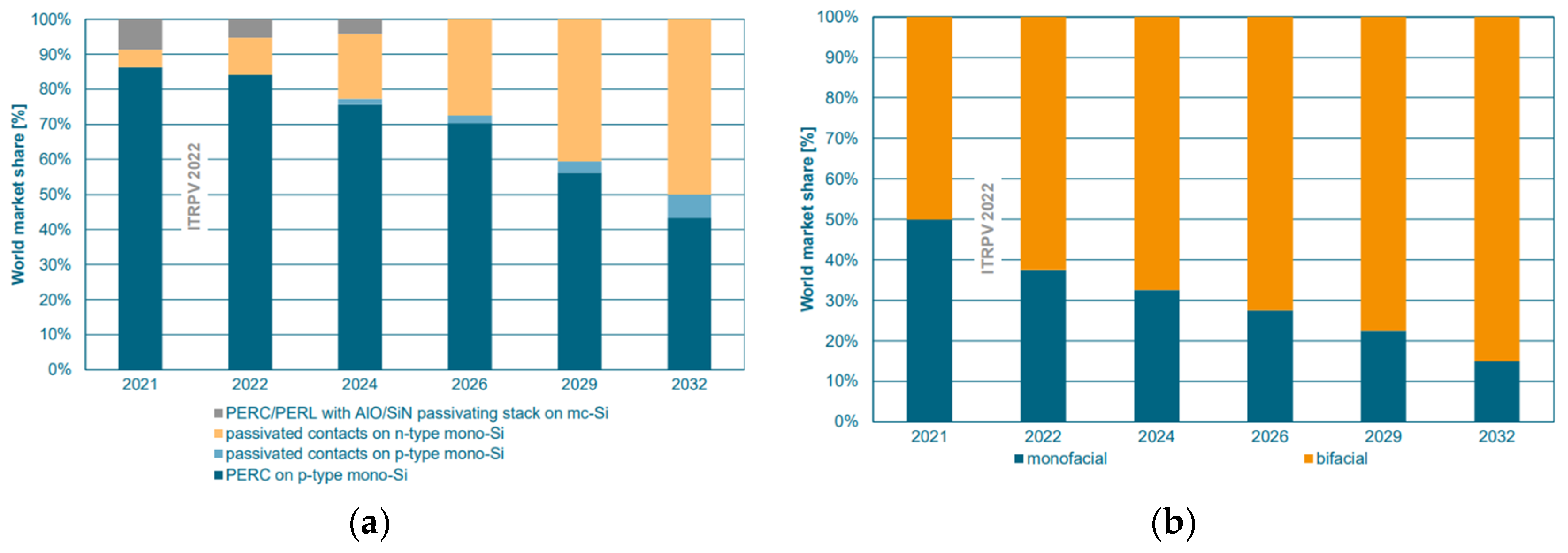
TOPCon cells convert more sunlight than P-type cells, which results in a higher cell and module efficiency. TOPCon cells can reach 28% efficiency (the PERC cell’s maximum efficiency is around 24%) [23]. TOPCon cells have a better power increase in bifacial modules than PERC modules. This is an important factor as bifacial solar modules are getting more and more popular on the market. Bifacial silicon solar cells can harvest light from both sides, increasing the overall energy yield. Figure 2 shows the current and forecast market share for c-Si cell concepts (Figure 2a) and bifacial cell technology (Figure 2b) [19].
Alongside the advancements achieved with TOPCon cells, silicon heterojunction (SHJ) cells also provide additional advantages compared to traditional homojunction cells and even efficiency gains, achieving remarkable efficiencies that even surpass TOPCon, reaching 26.81% [23]. This type of cell structure was originally developed by the Japanese company Sanyo in the 1990s [24], and already showed promising results, obtaining higher efficiencies than c-Si solar cell architectures of the time, particularly in terms of Voc and fill factor (FF). In the next few years, SHJ cells are expected to overtake Al-BSF solar cells in terms of their market share, becoming the second-most adopted commercial solar cell technology after PERC/TOPCon. This trend indicates a significant shift in the industry, with SHJ cells’ market share projected to increase to nearly 20% by 2032 [19].
SHJ cells are built by the deposition of stacks of intrinsic and doped hydrogenated amorphous silicon layers (a-Si:H) on the surface of crystalline silicon (c-Si) wafers [25]. The a-Si:H layer acts as a CSPC, thereby reducing carrier recombination between the silicon layer and the transparent conducting oxide (TCO) layer [26]. The latter aids lateral conduction and the formation of metal contacts. Because of the extra surface passivation provided by the a-Si:H layer, SHJ cells present higher Voc than PERC cells, namely 751 mV, and fill factors up to 86.59% for the cell demonstrated in [27]. Additionally, SHJ cells have a lower temperature coefficient than their PERC counterparts [28]. This implies that their efficiency will be less affected by temperature variations [29] and will perform better than PERC cells under realistic operating conditions [25].
Compared to Al-BSF, PERC and TOPCon structures, processing occurs at low temperatures in SHJ cells, typically under 250 °C [25]. The reason for this is the sensitivity of the a-Si:H layer to elevated temperatures—high temperatures deteriorate passivation layers, thereby reducing the minority carrier lifetime and efficiency [30]. In traditional homojunction structures, high-temperature processing is used for defect engineering, namely gettering, which removes unwanted metallic impurities in the bulk, and hydrogenation, i.e., hydrogen passivation of impurity-related and crystallographic defects. Because SHJ cells do not undergo this process, high-quality n-type Cz wafers are required for achieving high-efficiency SHJ cells. This argument was used in a recent review [25] to draw attention to defect engineering in SHJ cells to facilitate the use of lower-quality silicon wafers such as those made from low-lifetime SoG silicon [31], upgraded metallurgical-grade (UMG) silicon [32], and high-performance multicrystalline wafers [33]. Particularly in [31], it was shown how gettering plus hydrogenation can result in an increase of more than 70 mV for SHJ cells fabricated from low-lifetime SoG p-type Cz wafers. SHJ cells have demonstrated remarkable efficiencies, achieving 26.8% record efficiency. This value is only 3.2% lower than the theoretical limiting efficiency of silicon solar cells, i.e., 30%. This implies that the current single-junction solar cells are getting very close to their efficiency limit [3]. To overcome the Shockley–Queisser limit of single-junction solar cells, several strategies have been developed. The most prominent one is the tandem solar cell. Tandem cells, or multijunction, if there are more than two, are built by stacking single-junction solar cells in decreasing bandgap order [34]. This allows the structure to address what otherwise are unavoidable losses for single-junction solar cells: absorption and thermalization losses [35]. SHJ cells appear to be the perfect candidates for the bottom cell of a tandem stack, combined with perovskite solar cells at the top. Oxford PV reported a record one-sun conversion efficiency of 29.5% with two terminal perovskite/SHJ [36]. However, nonradiative recombination of the tandem stack and the high sensitivity of perovskite to low levels of humidity remain significant challenges that require further research and development [37]. Besides tandem cells, it is worth mentioning emerging areas such as the application of plasmonic nanostructures for improving light absorption and trapping in single-junction solar cells. The application of metallic nanoparticles in solar cells, particularly in perovskite solar cells, can lead to increased efficiency due to the plasmonic effect [38,39].
Research efforts have also focused on enhancing the durability and reliability of silicon solar cells. Improved materials, such as ARC and encapsulation materials, help to protect the cells from external factors like moisture, UV radiation and mechanical stress. This ensures that silicon solar cells can operate reliably for extended periods, delivering consistent electricity generation over their lifespan. Furthermore, recently, the potential of recycling solar cells and PV modules has gained attention and is becoming an important issue to make this renewable energy source greener and more sustainable.
A recent review on the recycling of PV modules [40] indicated that by 2050, 60 million tons of solar waste will be accumulated if no recycling strategies are developed. These authors presented various technical aspects of PV panel waste recycling and recovery, environmental safety and waste control. They also pointed out the importance of end-of-life (EOL) management for PV modules, which can create new industries and support economic value creation. PV EOL management also offers opportunities relating to each of the ‘3 Rs’ of sustainable waste management (i.e., reuse, recycle and repair). By 2030, the top three countries for cumulative PV waste are projected to include China, Germany and Japan [41]. The recycling of PV modules can involve various approaches, such as module reuse, component reuse, or material recovery. Tao et al. [42] emphasized the difficulty in establishing a consistent market for decommissioned modules in module reuse. Extracting components encounters challenges due to diverse structures, materials and variable cell efficiency. The common challenge across all cases is the expense associated with collecting, sorting and processing waste modules [42]. Several studies focus on enhancing the ease of disassembly in the design of the module, employing innovative technologies to maximize the reusability of valuable components [43,44]. Valuable materials found in solar panels include Si, aluminum (Al), silver (Ag), copper (Cu), tin (Sn), and the potentially harmful metal lead (Pb) [42]. Aluminum, glass, and silicon can be recycled through thermal and chemical methods. Mechanical separation extracts aluminum frames from solar panels, and thermal treatment easily recovers glass [45]. Despite relatively low prices, Al and glass remain profitable due to the substantial availability of recycled materials. Recovering more than 90% of silicon from original solar modules while meeting solar-grade standards involves separating different Si qualities. However, the present recovery rates for Ag and Cu are 74% and 83%, respectively, with the potential for improvement up to 95% [46].
In addition, regarding PV systems, it should be mentioned that besides roof-top installations and solar farms, new fields of installation have emerged like agrivoltaics, where PV modules are combined with crops growth, the dual use of solar energy for electricity- and food production [47], and floating PV. In the future, it is expected that land availability will be an issue (this applies to solar energy as well as to wind power, farming, building, etc.) and new technologies to tackle this aspect will be developed and used. This will trigger discussions about social acceptance and environmental, economic and social aspects.
In the following section, we will focus on and report on some of the industrial challenges for silicon solar cells.
3. Silicon Ingot Production for Solar Cells: Current State and Challenges
Crystalline silicon can be produced through two distinct methods. The monocrystalline PV cell method, established in the 1950s, involves the growth of cylindrical, single-crystal Si ingots measuring about 1.5–2 m in length. This is achieved using the Czochralski method, named after the Polish scientist Jan Czochralski [48]. Conversely, multicrystalline silicon is manufactured through directional solidification, also known as the vertical gradient freeze method. This technique is commonly employed to produce multicrystalline silicon ingots, with a yield ranging from 500 kg to 1 ton [49]. The method was initially proposed by Saito et al. [50].
3.1. Czochralski vs. Directional Solidification
The Czochralski (Cz) method for single-crystal growth was pioneered by Czochralski and has undergone significant advancements over the past 50 years, enabling the production of several hundred kilograms of ingots. A seed of a single crystal with a well-defined crystallographic orientation, either (100) or (111) orientations, is dipped into the melt and gradually pulled vertically to the surface, where silicon solidifies on the seed and adopts its orientation, as illustrated in Figure 3a. Notably, Dash’s practical procedure for dislocation elimination during the early stages of growth has enabled producing dislocation-free Cz ingots [51]. Moreover, precise control of the temperature gradient and the pulling rate is implemented to ensure the formation of dislocation-free crystals [52]. The dissolution of the quartz crucible into the melt leads to a relatively high oxygen concentration in the ingot. The main advantage of monocrystalline silicon cells is the high efficiency that results from a high-purity and defect-free microstructure. Currently, the Cz method has evolved into a highly sophisticated technique, governed by multiple parameters. This complexity adds further challenges in understanding and enhancing the current methodology.
The directional solidification (DS) or vertical gradient freeze (VGF) technique is used to produce multicrystalline silicon ingots which are distinguished by columnar grains that extend over height, as shown in Figure 3b. The SoG-Si feedstock is placed in a Si3N4-coated quartz crucible and heated under vacuum to 800 °C for degassing. Then, the furnace is filled with high-purity inert gas, typically 6N-argon, which is continuously injected to reduce the partial pressure of detrimental gases. Yuan et al. [54] proposed nitrogen gas as a cheap substitute for argon. They also claimed that nitrogen can be utilized as a doping source for silicon ingots where the concentration of dopants is controlled by adjusting the flow rate and the partial pressure of nitrogen in the furnace [54]. The nitrogen-doped Si wafers showed higher mechanical strength compared to the conventional wafers [54]. Increasing the flow rate of the inert gas during melting and solidification has a positive impact on reducing the melt contamination from the atmosphere [55] but it accelerates the coating degradation [56,57]. Also, less contamination and hence more homogenous ingots with no inclusions can be achieved by (i) rotating during the process [58,59] or stirring the melt with a magnetic field [60,61]. It has been found that the rotation of the crucible is beneficial to homogenize the concentration of light elements, namely carbon and nitrogen, in the melt under the saturation limit and avoid the precipitation of SiC and Si3N4 in the bulk [58,59]. Several approaches are based on the adjustment of the shape of the crucibles. Schmid et al. [62] developed a cone-shaped crucible which favors axial heat flux towards the cone tip and therefore yields a significant temperature gradient in this area. The optimization of different feedstock materials, as well as the seeding materials and sizes, has been also performed, aiming to enhance the quality and the microstate of the ingots [63,64,65,66]. A crucible with a notched bottom has been proposed to better control the grain growth at the beginning of the solidification [67]. Also, to prevent the metallic impurities from diffusion into the melt, several researchers have attempted to coat the crucible interior with different types of ultra-purity layers [68,69,70,71]. Moreover, Hendawi et al. [72,73] investigated key factors in silicon crystallization, including crucible types, coatings, and wetting principles, offering valuable insights for optimizing efficiency in the selection and use of crucibles and coatings.
Different crystallization techniques of Si ingots are suggested via the DS method. The traditional multi-crystalline Si ingots are produced by charging the feedstock directly in the Si3N4-coated crucible where liquid Si crystallizes on silicon nitride particles, resulting in the growth of large grains and high dislocation density. Later, Yang et al. [74] introduced the so-called high-performance mc-Si, where a seeding layer is used to ensure smaller but uniform grains. It has been found that the large fraction of grain boundaries suppresses the propagation of dislocations clusters in the ingots and hence enhances the cell performance [75]. Casting a monocrystalline Si ingot by VGF route was developed by [76], who placed mono-Si wafers with a crystal orientation of (100) as a seeding layer. However, a number of challenges have been found in mass scaling the mono-like ingots: (i) non-homogenous efficiency where top parts of the ingots provide low-performance cells, (ii) multi-crystallization and sub-grains close to the ingot walls, and (iii) the cost of the seeding layer [77,78]. Therefore, recent attempts have been reported to better control these defects and limit them close to the ingot walls by the Seed Manipulation for ARtificially controlled defect Technique (SMART) mono-like ingots [79] as well as the potential of reusing the seeding layer [77,80].
In this context, the Czochralski process has seen recent and rapid advancements, particularly in the size of grown ingots and the automation of the control process. The cost-effective mass production capabilities of the Czochralski process have thus caused a decline in the use of the directional solidification method in the industrial market, as was recently reported in the review by Ballif et al. [81].
3.2. Major Challenges of Cz Silicon Production
Despite its high level of maturity in the industrial sector, the Czochralski method (CZ) presents some challenges, especially when coping with increased demand. Below, we introduce some of these challenges.
3.2.1. Structure Loss
One of the crucial challenges in the Cz industry is losing the dislocation-free structure during growth, or what is termed as structure loss [82]. This problem is reported to occur in a considerable percentage of the grown ingots at different growth stages [83]. Remelting the infected ingots is the only available solution in the industry, which ultimately decreases the production yield. Several factors contribute to this structural loss, with the quality of the feedstock and crucible being of utmost importance. The potential causes of this failure are varied. Lanterne et al. [82,84] noted that the presence of a foreign particle or gas bubble at the solidification front can generate dislocations, eventually triggering a transition from a monocrystalline to a multicrystalline silicon structure. In contrast, Sortland et al. [85] argued that the presence of gas bubbles, or “pinholes”, does not necessarily lead to structure loss, as they are found in both well-structured and structurally compromised ingots. Additionally, it has been observed that the stress concentration around the pinhole remains below the level necessary for dislocation formation [85]. It was also found that the longer a crucible is used, the higher the likelihood is of experiencing structural loss due to crucible instability and the dissolution of silica particles in the melt [86]. Moreover, optimizing the pulling speed and stabilization time is crucial to mitigating potential disturbances during the growth process.
3.2.2. High Demand
It is expected that the PV capacity will more than quadruple from 150 GW in 2021 to 650 GW by 2030 [87]. The increasing demand for solar cells puts significant pressure on the silicon feedstock and ingot manufacturers. Consequently, producers are required to scale up the diameter of the ingots to meet the market’s needs. However, this increase in diameter presents an added challenge as it requires the utilization of larger crucibles, particularly since implementing a continuous growth process introduces considerable disturbances to the melt and increases the risk of contamination by foreign particles [88]. Currently, quartz crucibles are the sole option available to the industry. It has been demonstrated that larger crucibles carry a higher risk of defects, leading to reduced mechanical stability at high temperatures [89].
3.2.3. Cost and Efficiency
To enhance the efficiency of Cz silicon, it is necessary to increase its quality by producing consistent ingots with minimal variability. A crucial factor in achieving this is producing ingots with a uniform distribution of dopants. However, it is well-known that the current dominant doping elements in the market, i.e., phosphorus and gallium, have segregation coefficients that result in uneven dopant distribution within the ingots [90]. This leads to the need for remelting certain parts of the ingots due to doping concentrations falling below or exceeding the required levels. Therefore, additional costs are added due to wasted material and the inability to utilize the full potential of the ingot.
Also, the slow growth rate of Cz silicon ingots leads to higher energy consumption compared to alternative methods such as directional solidification [91]. However, cost reduction can be achieved through labor reduction and automation of the production line.
4. The Role of AI and How It Can Help to Solve Some of the PV Challenges
As data become an increasingly critical component across all industries, artificial intelligence (AI) and machine learning (ML) are playing a crucial role in advancing technological development and operational efficiency. AI and ML are revolutionizing a multitude of industries, from healthcare to finance. The PV industry is no exception to this trend. In recent years, more and more research has been completed to apply AI and, more specifically, ML across the PV value chain. To illustrate this, this section describes the novel application of ML in three key stages of the PV value chain: the analysis of silicon ingots, the optimization of solar cell design, and advanced defect characterization in solar cells.
The first application builds on the issues of structure loss described above in Section 3.2.1 Recent research [92] has demonstrated the impressive capabilities of ML, particularly deep learning (DL), in classifying the different types of structure loss occurring in CZ silicon ingots. The research proposes three pipelines based on DL and convolutional neural networks (CNN) to automate the task of classifying the three major types of structure loss. As illustrated in Figure 4, one of the proposed DL-based methods shows a remarkable accuracy progression as a function of training epochs (in the context of machine learning, an epoch refers to the one entire passing of training data through the algorithm). Remarkably, an accuracy of 92% was achieved with just 150 epochs of training and a limited dataset of 189 images, an amount considered relatively small in DL applications. This highlights the robustness and efficiency of the proposed solution. This advancement is significant as it suggests the potential for the automated classification of structure loss, a task traditionally reliant on human visual inspection. This automated approach could enhance accuracy, consistency, and speed in identifying structure loss, bringing about a transformative change in the PV industry.
Further down the value chain, ML and DL are also finding innovative applications. An example of this is [93], where neural networks and genetic algorithms were employed for the optimization of solar cell production lines, showing a potential increase in cell efficiency from 18.07% to 19.45%. Here, the authors noted that ML could outperform the traditional design of experiment (DoE) in optimizing the solar cell production line.
In the study, the authors designed a simulated production line of aluminum-back surface field (Al-BSF) solar cells, featuring 10 processing steps (such as saw damage etching, diffusion, and passivation) and 47 different process parameter inputs (such as etching duration, diffusion temperature, and deposition gas flow ratio). This number of parameters was chosen to demonstrate how ML could outperform traditional DoE, as the latter has severe limitations when the number of parameters surpasses 40 [94]. The outputs of the simulated experiment were used to produce solar cell recipes and efficiencies were determined using PC1D, a finite-element numerical solver used for modelling solar cells [95]. Systematically varying parameters in the recipe allowed the authors to generate a dataset containing 400,000 cells. Several ML algorithms were trained on this dataset to learn to predict the cell’s efficiency given an input set of parameters (recipe). A genetic algorithm was applied to the best-performing method to find a recipe that could result in higher-efficiency cells. The recipe was then varied to obtain a new dataset and the process was repeated. After five iterations, the initial maximum efficiency of 18.07 ± 0.29% had increased to 19.45 ± 0.31%.
The increase in efficiency is remarkable and although the pipeline was applied to Al-BSF, the authors noted that the proposed method could be extended to other cell structures, such as passivated emitter and rear contact (PERC) or silicon heterojunction (SHJ), thereby taking the PV industry one step closer to Industry 4.0.
Another exciting application of ML to the solar cell value chain is described in [96]. Here, the authors proposed an attention-based [97] framework to automatically detect defects in electroluminescence (EL) images.
In recent years, DL-based frameworks have become increasingly popular for defect detection in EL images [98,99], surpassing the accuracy of traditional computer vision methods. Ref. [96] builds on previous work that uses CNN for this task and introduces enhancements based on attention mechanisms. The work features the development of a novel Complementary Attention Network (CAN), which is used for removing background features and highlighting defects. The authors proposed combining this CAN with a Region Proposal Network [100], thereby implementing what they define as the novel Region Proposal Attention Network (RPAN). This RPAN is combined with a CNN, resulting in a framework that can efficiently detect defects, even in complex heterogeneous backgrounds. The authors tested the proposed method on an EL dataset containing 3629 images, and the results were remarkable, not only obtaining accuracies surpassing 95% but also outperforming other previous detectors.
The work presented in [96] has set the stage for further innovative research. A recent example of this is described in Ref. [101]. Here, the authors incorporated the RPAN method described above in a new DL framework for loss analysis based on luminescence images. This advanced framework consists of three modules: efficiency prediction, using the LumiNet CNN [102]; defect localization using the RPAN [96]; and defect removal and reconstruction using generative adversarial networks (GANs). Ref. [101] focuses on the GAN part. The presented results are remarkable, as the generator completed the patch, and was able to restore the busbars and background luminescence. Not only that but also the generator was successful in eliminating defects from the image and preserving features in the unmasked regions. This approach showed potential in aiding defect identification and enabling large-scale, quantitative analysis of luminescence image data.
With ML and DL proving instrumental in addressing issues like structure loss and solar cell design optimization, it becomes clear that the incorporation of these AI tools into the PV industry can drive significant operational improvements. As the field continues to evolve, there will be more opportunities to use these technologies to overcome other complex challenges within the PV value chain.
5. Conclusions
In this work, we have provided an overview of the status of silicon solar cell manufacturing. Our discussion has ranged from feedstock production to ingot processing to solar cell fabrication and included aspects on recycling and AI.
We first focused on the challenges and advancements in silicon ingot production for solar cells, particularly in the Czochralski (Cz) and directional solidification (DS) methods. The Cz method, despite recent improvements, faces issues such as structure loss, meeting demand for larger ingots, and ensuring uniform dopant distribution. Challenges in scaling up ingot diameter increase contamination risks and production costs. The slow growth rate also contributes to higher energy consumption. The DS method, producing multicrystalline silicon ingots, incorporates various techniques for quality enhancement. However, recent advancements in Cz technology have reduced the use of DS in the industrial market.
We then reviewed the development of silicon solar cell architectures. We have discussed modern silicon-based solar cell structures, including TOPCon and SHJ, and highlighted how applying preprocessing techniques traditionally used in homojunction solar cells, such as defect engineering, to SHJ cells can lead to notable improvements in Voc and overall efficiency. We have discussed how tandem structures built from a SHJ bottom cell combined with perovskite solar cells at the top can be perfect candidates for surpassing the single junction efficiency limit, and how metallic nanoparticles may enhance light absorption in perovskite solar cells.
In our discussion, we also emphasized the growing importance of recycling and sustainability aspects in the PV sector, including the steps of collecting, disassembling, sorting, and processing of PV module waste. These processes have the potential of increasing the recovery of key materials such as Si, Al, glass, Ag, and Cu.
Finally, we have discussed how artificial intelligence and machine learning may provide innovative solutions to overcome some of challenges that the PV industry faces. Our discussion has focused on the novel application of machine learning in the analysis of structure loss in silicon ingots, the optimization of solar cell design, and advanced defect characterization in solar cells. These applications show the crucial role that artificial intelligence is playing in advancing technological development and operational efficiency.
Overall, this work provides a broad overview of the current state of silicon solar cells from crystallization to solar cell manufacturing, and highlights the continuous effort to improve cell efficiency. It is clear that artificial intelligence is going to have an increasing role in PV industry and research.
Author Contributions
M.D.S.: conceptualization, methodology, writing-original draft preparation; writing-review and editing. R.H.: conceptualization, methodology, writing-original draft preparation; writing-review and editing. A.S.G.: conceptualization, methodology, writing-original draft preparation; writing-review and editing. All authors have read and agreed to the published version of the manuscript.
Funding
This research was funded by the Norwegian Research Center for Sustainable Solar Cell Technology (FME SUSOLTECH, project number 275639/E20). The center is co-sponsored by the Research Council of Norway and its research and industry partners.
Data Availability Statement
No new data were created or analyzed in this study. Data sharing is not applicable to this article.
Conflicts of Interest
The authors declare no conflict of interest. Alfredo Sanchez Garcia is still employed by SINTEF AS. SINTEF AS is a non-profit research institution. Therefore, Alfredo Sanchez Garcia has no conflict of interest to declare either.
References
- Fraunhofer Institute for Solar Energy Systems, ISE. Photovoltaics Report; ISE: Freiburg, Germany, 2023. [Google Scholar]
- Fernández, L. Cumulative Installed Solar Pv Capacity Worldwide from 2000 to 2022. Available online: https://www.statista.com/statistics/280220/global-cumulative-installed-solar-pv-capacity/ (accessed on 20 December 2023).
- Shockley, W.; Queisser, H.J. Detailed Balance Limit of Efficiency of p-n Junction Solar Cells. J. Appl. Phys. 1961, 32, 510–519. [Google Scholar] [CrossRef]
- Green, M.A.; Dunlop, E.D.; Hohl-Ebinger, J.; Yoshita, M.; Kopidakis, N.; Bothe, K.; Hinken, D.; Rauer, M.; Hao, X. Solar cell efficiency tables (Version 60). Prog. Photovolt. Res. Appl. 2022, 30, 687–701. [Google Scholar] [CrossRef]
- Woditsch, P.; Koch, W. Solar grade silicon feedstock supply for PV industry. Sol. Energy Mater. Sol. Cells 2002, 72, 11–26. [Google Scholar] [CrossRef]
- Yuge, N.; Sakaguchi, Y.; Terashima, H.; Aratani, F. Purification of silicon by directional solidification. Nippon. Kinzoku Gakkaishi/J. Jpn. Inst. Met. 1997, 61, 1094–1100. [Google Scholar] [CrossRef]
- Yuge, N.; Hanazawa, K.; Hiwasa, S.; Kato, Y. Removal of Metal Impurities in Molten Silicon by Directional Solidification with Electron Beam Heating. J. Jpn. Inst. Met. 2003, 67, 575–582. [Google Scholar] [CrossRef]
- Liu, T.; Dong, Z.; Zhao, Y.; Wang, J.; Chen, T.; Xie, H.; Li, J.; Ni, H.; Huo, D. Purification of metallurgical silicon through directional solidification in a large cold crucible. J. Cryst. Growth 2012, 355, 145–150. [Google Scholar] [CrossRef]
- Martorano, M.A.; Neto, J.B.F.; Oliveira, T.S.; Tsubaki, T.O. Refining of metallurgical silicon by directional solidification. Mater. Sci. Eng. B 2011, 176, 217–226. [Google Scholar] [CrossRef]
- Jiang, D.; Ren, S.; Shi, S.; Dong, W.; Qiu, J.; Tan, Y.; Li, J. Phosphorus Removal from Silicon by Vacuum Refiningand Directional Solidification. J. Electron. Mater. 2014, 43, 314–319. [Google Scholar] [CrossRef]
- Qiu, S.; Wen, S.; Fang, M.; Zhang, L.; Gan, C.; Jiang, D.; Tan, Y.; Li, J.; Luo, X. Process parameters influence on the growth rate during silicon purification by vacuum directional solidification. Vacuum 2016, 125, 40–47. [Google Scholar] [CrossRef]
- Pizzini, S. Towards solar grade silicon: Challenges and benefits for low cost photovoltaics. Sol. Energy Mater. Sol. Cells 2010, 94, 1528–1533. [Google Scholar] [CrossRef]
- Li, X.; Wu, J.; Xu, M.; Ma, W. Separation and purification of silicon from cutting kerf-loss slurry waste by electromagnetic and slag treatment technology. J. Clean. Prod. 2019, 211, 695–703. [Google Scholar] [CrossRef]
- Ning, S.; Shuo, D. Thin Film Deposition Technologies and Application in Photovoltaics. In Thin Films; Dongfang, Y., Ed.; IntechOpen: Rijeka, Croatia, 2022. [Google Scholar]
- Zhao, Y.; Procel, P.; Han, C.; Cao, L.; Yang, G.; Özkol, E.; Alcañiz, A.; Kovačević, K.; Limodio, G.; Santbergen, R.; et al. Strategies for realizing high-efficiency silicon heterojunction solar cells. Sol. Energy Mater. Sol. Cells 2023, 258, 112413. [Google Scholar] [CrossRef]
- Mandelkorn, J.; Lamneck, J.H. Simplified fabrication of back surface electric field silicon cells and novel characteristics of such cells. Sol. Cells 1990, 29, 121–130. [Google Scholar] [CrossRef]
- Kim, K.H.; Park, C.S.; Lee, J.D.; Lim, J.Y.; Yeon, J.M.; Kim, I.H.; Lee, E.J.; Cho, Y.H. Record high efficiency of screen-printed silicon aluminum back surface field solar cell: 20.29%. Jpn. J. Appl. Phys. 2017, 56, 08MB25. [Google Scholar] [CrossRef]
- Blakers, A.W.; Wang, A.; Milne, A.M.; Zhao, J.; Green, M.A. 22.8% efficient silicon solar cell. Appl. Phys. Lett. 1989, 55, 1363–1365. [Google Scholar] [CrossRef]
- International Technology Roadmap for Photovoltaic (ITRPV); VDMA: Frankfurt am Main, Germany, 2022.
- Zhao, J.; Wang, A.; Green, M.A. 24% efficient PERL structure silicon solar cells. In Proceedings of the IEEE Conference on Photovoltaic Specialists, Kissimmee, FL, USA, 21–25 May 1990; Volume 331, pp. 333–335. [Google Scholar]
- Zhao, J.; Wang, A.; Green, M.A. 24·5% Efficiency silicon PERT cells on MCZ substrates and 24·7% efficiency PERL cells on FZ substrates. Prog. Photovolt. Res. Appl. 1999, 7, 471–474. [Google Scholar] [CrossRef]
- JinkoSolar’s High-efficiency N-Type Monocrystalline Silicon Solar Cell Sets Our New Record with Maximum Conversion Efficiency of 26.4%. Available online: https://www.jinkosolar.com/en/site/newsdetail/1827 (accessed on 10 January 2024).
- The Complete Guide to TOPCon Technology. Available online: https://www.eco-greenenergy.com/the-complete-guide-to-topcon-technology/ (accessed on 23 December 2023).
- Tanaka, M.; Taguchi, M.; Matsuyama, T.; Sawada, T.; Tsuda, S.; Nakano, S.; Hanafusa, H.; Kuwano, Y. Development of New a-Si/c-Si Heterojunction Solar Cells: ACJ-HIT (Artificially Constructed Junction-Heterojunction with Intrinsic Thin-Layer). Jpn. J. Appl. Phys. 1992, 31, 3518. [Google Scholar] [CrossRef]
- Wright, M.; Stefani, B.V.; Soeriyadi, A.; Basnet, R.; Sun, C.; Weigand, W.; Yu, Z.; Holman, Z.; Macdonald, D.; Hallam, B. Progress with Defect Engineering in Silicon Heterojunction Solar Cells. Phys. Status Solidi (RRL)–Rapid Res. Lett. 2021, 15, 2100170. [Google Scholar] [CrossRef]
- Jiang, K.; Liu, W.; Yang, Y.; Yan, Z.; Huang, S.; Li, Z.; Li, X.; Zhang, L.; Liu, Z. Functions of oxygen atoms in hydrogenated amorphous silicon oxide layers for rear-emitter silicon heterojunction solar cells. J. Mater. Sci. Mater. Electron. 2022, 33, 416–426. [Google Scholar] [CrossRef]
- Lin, H.; Yang, M.; Ru, X.; Wang, G.; Yin, S.; Peng, F.; Hong, C.; Qu, M.; Lu, J.; Fang, L.; et al. Silicon heterojunction solar cells with up to 26.81% efficiency achieved by electrically optimized nanocrystalline-silicon hole contact layers. Nat. Energy 2023, 8, 789–799. [Google Scholar] [CrossRef]
- Dupré, O.; Vaillon, R.; Green, M.A. Thermal Behavior of Photovoltaic Devices; Springer: Cham, Germany, 2017. [Google Scholar]
- Garcia, A.S.; Kristensen, S.T.; Strandberg, R. Analytical Modeling of the Temperature Sensitivity of the Maximum Power Point of Solar Cells. IEEE J. Photovolt. 2022, 12, 1237–1242. [Google Scholar] [CrossRef]
- Stefaan, D.W.; Kondo, M. Boron-Doped a-Si:H/C-Si Interface Passivation: Degradation Mechanism. Appl. Phys. Lett. 2007, 91, 112109. [Google Scholar] [CrossRef]
- Hallam, B.; Chen, D.; Shi, J.; Einhaus, R.; Holman, Z.C.; Wenham, S. Pre-Fabrication Gettering and Hydrogenation Treatments for Silicon Heterojunction Solar Cells: A Possible Path to >700 mV Open-Circuit Voltages Using Low-Lifetime Commercial-Grade p-Type Czochralski Silicon. Sol. RRL 2018, 2, 1700221. [Google Scholar] [CrossRef]
- Vicari Stefani, B.; Weigand, W.; Wright, M.; Soeriyadi, A.; Yu, Z.; Kim, M.; Chen, D.; Holman, Z.; Hallam, B. P-type Upgraded Metallurgical-Grade Multicrystalline Silicon Heterojunction Solar Cells with Open-Circuit Voltages over 690 mV. Phys. Status Solidi A 2019, 216, 1900319. [Google Scholar] [CrossRef]
- Chen, D.; Kim, M.; Shi, J.; Vicari Stefani, B.; Yu, Z.; Liu, S.; Einhaus, R.; Wenham, S.; Holman, Z.; Hallam, B. Defect engineering of p-type silicon heterojunction solar cells fabricated using commercial-grade low-lifetime silicon wafers. Prog. Photovolt. Res. Appl. 2021, 29, 1165–1179. [Google Scholar] [CrossRef]
- Martí, A.; Araújo, G.L. Limiting efficiencies for photovoltaic energy conversion in multigap systems. Sol. Energy Mater. Sol. Cells 1996, 43, 203–222. [Google Scholar] [CrossRef]
- Hirst, L.C.; Ekins-Daukes, N.J. Fundamental losses in solar cells. Prog. Photovolt. Res. Appl. 2011, 19, 286–293. [Google Scholar] [CrossRef]
- Best Research-Cell Efficiency Chart. NREL Laboratory Cell Efficiency: 2023. Available online: https://www.nrel.gov/pv/cell-efficiency.html (accessed on 10 January 2024).
- Li, X.; Xu, Q.; Yan, L.; Ren, C.; Shi, B.; Wang, P.; Mazumdar, S.; Hou, G.; Zhao, Y.; Zhang, X. Silicon heterojunction-based tandem solar cells: Past, status, and future prospects. Nanophotonics 2020, 10, 2001–2022. [Google Scholar] [CrossRef]
- Jacak, J.E.; Jacak, W.A. Routes for Metallization of Perovskite Solar Cells. Materials 2022, 15, 2254. [Google Scholar] [CrossRef]
- Jacak, W.A. Quantum Nano-Plasmonics; Cambridge University Press: Cambridge, UK, 2020. [Google Scholar]
- Divya, A.; Adish, T.; Kaustubh, P.; Zade, P.S. Review on recycling of solar modules/panels. Sol. Energy Mater. Sol. Cells 2023, 253, 112151. [Google Scholar] [CrossRef]
- Chowdhury, M.S.; Rahman, K.S.; Chowdhury, T.; Nuthammachot, N.; Techato, K.; Akhtaruzzaman, M.; Tiong, S.K.; Sopian, K.; Amin, N. An overview of solar photovoltaic panels’ end-of-life material recycling. Energy Strategy Rev. 2020, 27, 100431. [Google Scholar] [CrossRef]
- Tao, M.; Fthenakis, V.; Ebin, B.; Steenari, B.-M.; Butler, E.; Sinha, P.; Corkish, R.; Wambach, K.; Simon, E.S. Major challenges and opportunities in silicon solar module recycling. Prog. Photovolt. Res. Appl. 2020, 28, 1077–1088. [Google Scholar] [CrossRef]
- Tao, J.; Yu, S. Review on feasible recycling pathways and technologies of solar photovoltaic modules. Sol. Energy Mater. Sol. Cells 2015, 141, 108–124. [Google Scholar] [CrossRef]
- Doi, T.; Igari, S.; Tsuda, I. Development of a recyclable PV-module-expansion to multi-cells modules. In Proceedings of the Conference Record of the Thirty-First IEEE Photovoltaic Specialists Conference, Lake Buena Vista, FL, USA, 3–7 January 2005; pp. 1773–1776. [Google Scholar]
- Jung, B.; Park, J.; Seo, D.; Park, N. Sustainable System for Raw-Metal Recovery from Crystalline Silicon Solar Panels: From Noble-Metal Extraction to Lead Removal. ACS Sustain. Chem. Eng. 2016, 4, 4079–4083. [Google Scholar] [CrossRef]
- Huang, W.-H.; Shin, W.J.; Wang, L.; Sun, W.-C.; Tao, M. Strategy and technology to recycle wafer-silicon solar modules. Sol. Energy 2017, 144, 22–31. [Google Scholar] [CrossRef]
- Manni, M.; Aghaei, M.; Sizkouhi, A.M.M.; Kumar, R.R.R.; Stølen, R.; Steen-Hansen, A.E.; Di Sabatino, M.; Moazami, A.; Völler, S.; Jelle, B.P.; et al. Solar Energy in the Built Environment. In Reference Module in Earth Systems and Environmental Sciences; Elsevier: Amsterdam, The Netherlands, 2023. [Google Scholar]
- Yu, X.; Yang, D. Growth of Crystalline Silicon for Solar Cells: Czochralski Si. In Handbook of Photovoltaic Silicon; Yang, D., Ed.; Springer: Berlin/Heidelberg, Germany, 2019; pp. 129–174. [Google Scholar]
- Ganesh, R.B.; Ryningen, B.; Syvertsen, M.; Øvrelid, E.; Saha, I.; Tathgar, H.; Rajeswaran, G. Growth and characterization of multicrystalline silicon ingots by directional solidification for solar cell applications. Energy Procedia 2011, 8, 371–376. [Google Scholar] [CrossRef]
- Saito, T.; Shimura, A.; Ichikawa, S. A new directional solidification technique for polycrystalline solar grade silicon. In Proceedings of the 15th Photovoltaic Specialists Conference, Kissimmee, FL, USA, 12–15 May 1981. [Google Scholar]
- Dash, W.C. Growth of Silicon Crystals Free from Dislocations. J. Appl. Phys. 2004, 30, 459–474. [Google Scholar] [CrossRef]
- Goetzberger, A.; Hebling, C.; Schock, H.-W. Photovoltaic materials, history, status and outlook. Mater. Sci. Eng. R Rep. 2003, 40, 1–46. [Google Scholar] [CrossRef]
- Hendawi, R. Reusable Crucible Materials and Coatings for Photovoltaic Silicon Applications. PhD Thesis, NTNU, Trondheim, Norway, 2021. [Google Scholar]
- Yuan, S.; Hu, D.; Yu, X.; Zhang, F.; Luo, H.; He, L.; Yang, D. Controllable Nitrogen Doping in Multicrystalline Silicon by Casting Under Low Cost Ambient Nitrogen. Silicon 2018, 10, 1717–1722. [Google Scholar] [CrossRef]
- Qi, X.; Xue, Y.; Su, W.; Ma, W.; Liu, L. Effect of Argon Flow on Oxygen and Carbon Coupled Transport in an Industrial Directional Solidification Furnace for Crystalline Silicon Ingots. Crystals 2021, 11, 421. [Google Scholar] [CrossRef]
- Hendawi, R.; Ciftja, A.; Arnberg, L.; Di Sabatino, M. Kinetics of silicon nitride coatings degradation and its influence on liquid infiltration in PV silicon crystallization processes. Sol. Energy Mater. Sol. Cells 2021, 230, 111190. [Google Scholar] [CrossRef]
- Hendawi, R.; Arnberg, L.; Di Sabatino, M. Effect of gas atmospheres on the interactions between liquid silicon and coated graphite substrates. Sol. Energy Mater. Sol. Cells 2022, 235, 111452. [Google Scholar] [CrossRef]
- Bellmann, M.P.; Meese, E.A.; Arnberg, L. Effect of accelerated crucible rotation on the segregation of impurities in vertical Bridgman growth of multi-crystalline silicon. J. Cryst. Growth 2011, 318, 239–243. [Google Scholar] [CrossRef]
- Bellmann, M.P.; Meese, E.A. Effect of steady crucible rotation on the segregation of impurities in vertical Bridgman growth of multi-crystalline silicon. J. Cryst. Growth 2011, 333, 1–6. [Google Scholar] [CrossRef]
- Pätzold, O.; Grants, I.; Wunderwald, U.; Jenkner, K.; Cröll, A.; Gerbeth, G. Vertical gradient freeze growth of GaAs with a rotating magnetic field. J. Cryst. Growth 2002, 245, 237–246. [Google Scholar] [CrossRef]
- Kiessling, F.M.; Büllesfeld, F.; Dropka, N.; Frank-Rotsch, C.; Müller, M.; Rudolph, P. Characterization of mc-Si directionally solidified in travelling magnetic fields. J. Cryst. Growth 2012, 360, 81–86. [Google Scholar] [CrossRef]
- Schmid, E.; Poklad, A.; Heinze, V.; Meier, D.; Pätzold, O.; Stelter, M. Growth of multicrystalline silicon in a cone-shaped crucible. J. Cryst. Growth 2015, 416, 1–7. [Google Scholar] [CrossRef]
- Reimann, C.; Trempa, M.; Lehmann, T.; Rosshirt, K.; Stenzenberger, J.; Friedrich, J.; Hesse, K.; Dornberger, E. Influence of different seed materials on multi-crystalline silicon ingot properties. J. Cryst. Growth 2016, 434, 88–95. [Google Scholar] [CrossRef]
- Schwanke, S.; Trempa, M.; Reimann, C.; Kuczynski, M.; Schroll, G.; Sans, J.; Friedrich, J. Production of high performance multi-crystalline silicon ingots for PV application by using contamination-free SixNy seed particles. J. Cryst. Growth 2019, 522, 151–159. [Google Scholar] [CrossRef]
- Huang, C.; Zhang, H.; Yuan, S.; Wu, Y.; Zhang, X.; You, D.; Wang, L.; Yu, X.; Wan, Y.; Yang, D. Multicrystalline silicon assisted by polycrystalline silicon slabs as seeds. Sol. Energy Mater. Sol. Cells 2018, 179, 312–318. [Google Scholar] [CrossRef]
- Coletti, G.; Kvande, R.; Mihailetchi, V.D.; Geerligs, L.J.; Arnberg, L.; Øvrelid, E.J. Effect of iron in silicon feedstock on p- and n-type multicrystalline silicon solar cells. J. Appl. Phys. 2008, 104, 104913. [Google Scholar] [CrossRef]
- Li, T.F.; Yeh, K.M.; Hsu, W.C.; Lan, C.W. High-quality multi-crystalline silicon (mc-Si) grown by directional solidification using notched crucibles. J. Cryst. Growth 2011, 318, 219–223. [Google Scholar] [CrossRef]
- Zhang, H.; Hu, D.; Zhong, D.; Huang, C.; Yuan, S.; You, D.; Zhang, X.; Wan, Y. The effect of diffusion barrier on minority carrier lifetime improvement of seed assisted cast silicon ingot. J. Cryst. Growth 2020, 541, 125684. [Google Scholar] [CrossRef]
- Trempa, M.; Sturm, F.; Kranert, C.; Schwanke, S.; Reimann, C.; Friedrich, J.; Schenk, C. Impact of different SiO2 diffusion barrier layers on lifetime distribution in multi-crystalline silicon ingots. J. Cryst. Growth 2020, 532, 125378. [Google Scholar] [CrossRef]
- Lei, Q.; He, L.; Ao, P.; Li, X.; Liu, S.; Zhang, X.; Liao, L.; Zhou, L. Study on reducing the contamination of metal impurities for casting silicon ingots by using non-oxide crucible barrier layer. Sol. Energy Mater. Sol. Cells 2021, 231, 111132. [Google Scholar] [CrossRef]
- Wolny, F.; Krause, A.; Müller, M.; Fischer, G.; Neuhaus, H. Reduced metal contamination from crucible and coating using a silicon nitride based diffusion barrier for the growth of cast quasi-single crystalline silicon ingots. J. Cryst. Growth 2019, 514, 49–53. [Google Scholar] [CrossRef]
- Hendawi, R.; Arnberg, L.; Di Sabatino, M. Crucibles and Coatings for Silicon Melting and Crystallization: An In-Depth Review of Key Considerations. Prog. Mater. Sci. 2023; in press. [Google Scholar]
- Hendawi, R.; Arnberg, L.; Di Sabatino, M. Novel coatings for graphite materials in PV silicon applications: A study of the surface wettability and interface interactions. Sol. Energy Mater. Sol. Cells 2022, 234, 111422. [Google Scholar] [CrossRef]
- Yang, Y.M.; Yu, A.; Hsu, B.; Hsu, W.C.; Yang, A.; Lan, C.W. Development of high-performance multicrystalline silicon for photovoltaic industry. Prog. Photovolt. Res. Appl. 2015, 23, 340–351. [Google Scholar] [CrossRef]
- Stokkan, G.; Hu, Y.; Mjøs, Ø.; Juel, M. Study of evolution of dislocation clusters in high performance multicrystalline silicon. Sol. Energy Mater. Sol. Cells 2014, 130, 679–685. [Google Scholar] [CrossRef]
- Stoddard, N.; Wu, B.; Witting, I.; Wagener, M.C.; Park, Y.; Rozgonyi, G.A.; Clark, R. Casting Single Crystal Silicon: Novel Defect Profiles from BP Solar’s Mono2 TM Wafers. Solid State Phenom. 2008, 131–133, 1–8. [Google Scholar]
- Guerrero, I.; Parra, V.; Carballo, T.; Black, A.; Miranda, M.; Cancillo, D.; Moralejo, B.; Jiménez, J.; Lelièvre, J.-F.; del Cañizo, C. About the origin of low wafer performance and crystal defect generation on seed-cast growth of industrial mono-like silicon ingots. Prog. Photovolt. Res. Appl. 2014, 22, 923–932. [Google Scholar] [CrossRef]
- Song, L.; Yu, X. Defect engineering in cast mono-like silicon: A review. Prog. Photovolt. Res. Appl. 2021, 29, 294–314. [Google Scholar] [CrossRef]
- Takahashi, I.; Joonwichien, S.; Iwata, T.; Usami, N. Seed manipulation for artificially controlled defect technique in new growth method for quasi-monocrystalline Si ingot based on casting. Appl. Phys. Express 2015, 8, 105501. [Google Scholar] [CrossRef]
- He, L.; Yuan, S.; Xu, Y.; Lei, Q.; Mao, W.; Luo, H.; He, X.; Li, X.; Wang, L.; Yang, D.; et al. Evaluation of large-scale recycled seed for cast monocrystalline silicon: Defect multiplication mechanisms and feasibility. Sol. Energy Mater. Sol. Cells 2021, 230, 111266. [Google Scholar] [CrossRef]
- Ballif, C.; Haug, F.-J.; Boccard, M.; Verlinden, P.J.; Hahn, G. Status and perspectives of crystalline silicon photovoltaics in research and industry. Nat. Rev. Mater. 2022, 7, 597–616. [Google Scholar] [CrossRef]
- Lanterne, A.; Gaspar, G.; Hu, Y.; Øvrelid, E.; Sabatino, M.D. Investigation of different cases of dislocation generation during industrial Cz silicon pulling. Phys. Status Solidi C 2016, 13, 827–832. [Google Scholar] [CrossRef]
- Hendawi, R.; Di Sabatino, M. Analyzing structure loss in Czochralski silicon growth: Root causes investigation through surface examination. J. Cryst. Growth 2024, 629, 127564. [Google Scholar] [CrossRef]
- Lanterne, A.; Gaspar, G.; Hu, Y.; Øvrelid, E.; Di Sabatino, M. Characterization of the loss of the dislocation-free growth during Czochralski silicon pulling. J. Cryst. Growth 2017, 458, 120–128. [Google Scholar] [CrossRef]
- Sortland, Ø.S.; Øvrelid, E.J.; M’Hamdi, M.; Di Sabatino, M. Investigation of pinholes in Czochralski silicon ingots in relation to structure loss. J. Cryst. Growth 2019, 510, 1–6. [Google Scholar] [CrossRef]
- Sortland, Ø.S.; Jomâa, M.; M’Hamdi, M.; Øvrelid, E.J.; Di Sabatino, M. Statistical analysis of structure loss in Czochralski silicon growth. AIP Conf. Proc. 2019, 2147, 100002. [Google Scholar]
- World Energy Outlook; IRENA: Masdar City, United Arab Emirates, 2022.
- Warden, G.K.; Juel, M.; Gaweł, B.A.; Di Sabatino, M. Recent developments on manufacturing and characterization of fused quartz crucibles for monocrystalline silicon for photovoltaic applications. Open Ceram. 2023, 13, 100321. [Google Scholar] [CrossRef]
- Peng, L.; Qin, S.; Gu, X. Effects of melting parameters and quartz purity on silica glass crucible produced by arc method. Eng. Res. Express 2020, 2, 015046. [Google Scholar] [CrossRef]
- Forster, M.; Fourmond, E.; Einhaus, R.; Lauvray, H.; Kraiem, J.; Lemiti, M. Ga co-doping in Cz-grown silicon ingots to overcome limitations of B and P compensated silicon feedstock for PV applications. Phys. Status Solidi C 2011, 8, 678–681. [Google Scholar] [CrossRef]
- Schubert, M.C.; Schindler, F.; Benick, J.; Riepe, S.; Krenckel, P.; Richter, A.; Müller, R.; Hammann, B.; Nold, S. The potential of cast silicon. Sol. Energy Mater. Sol. Cells 2021, 219, 110789. [Google Scholar] [CrossRef]
- Sanchez Garcia, A.; Hendawi, R.; Di Sabatino, M. Machine learning methods for structure loss classification in Czochralski silicon ingots. Submitt. Cryst. Growth Des. 2023; in press. [Google Scholar]
- Buratti, Y.; Eijkens, C.; Hameiri, Z. Optimization of Solar Cell Production Lines Using Neural Networks and Genetic Algorithms. ACS Appl. Energy Mater. 2020, 3, 10317–10322. [Google Scholar] [CrossRef]
- Roy, R.K. Design of Experiments Using The Taguchi Approach: 16 Steps to Product and Process Improvement; John Wiley & Sons: Hoboken, NJ, USA, 2001. [Google Scholar]
- Haug, H.; Greulich, J. PC1Dmod 6.2–Improved Simulation of c-Si Devices with Updates on Device Physics and User Interface. Energy Procedia 2016, 92, 60–68. [Google Scholar] [CrossRef]
- Su, B.; Chen, H.; Chen, P.; Bian, G.; Liu, K.; Liu, W. Deep Learning-Based Solar-Cell Manufacturing Defect Detection With Complementary Attention Network. IEEE Trans. Ind. Inform. 2021, 17, 4084–4095. [Google Scholar] [CrossRef]
- Vaswani, A.; Shazeer, N.; Parmar, N.; Uszkoreit, J.; Jones, L.; Gomez, A.N.; Kaiser, L.; Polosukhin, I. Attention Is All You Need. arXiv 2023, arXiv:1706.03762. [Google Scholar]
- Chen, F.C.; Jahanshahi, M.R. NB-CNN: Deep Learning-Based Crack Detection Using Convolutional Neural Network and Naïve Bayes Data Fusion. IEEE Trans. Ind. Electron. 2018, 65, 4392–4400. [Google Scholar] [CrossRef]
- Deitsch, S.; Christlein, V.; Berger, S.; Buerhop-Lutz, C.; Maier, A.; Gallwitz, F.; Riess, C. Automatic classification of defective photovoltaic module cells in electroluminescence images. Sol. Energy 2019, 185, 455–468. [Google Scholar] [CrossRef]
- Han, H.; Gao, C.; Zhao, Y.; Liao, S.; Tang, L.; Li, X. Polycrystalline silicon wafer defect segmentation based on deep convolutional neural networks. Pattern Recognit. Lett. 2020, 130, 234–241. [Google Scholar] [CrossRef]
- Buratti, Y.; Abdullah-Vetter, Z.; Sowmya, A.; Trupke, T.; Hameiri, Z. A Deep Learning Approach for Loss-Analysis from Luminescence Images. In Proceedings of the 2021 IEEE 48th Photovoltaic Specialists Conference (PVSC), Fort Lauderdale, FL, USA, 20–25 June 2021. [Google Scholar]
- Buratti, Y.; Sowmya, A.; Evans, R.; Trupke, T.; Hameiri, Z. Half and full solar cell efficiency binning by deep learning on electroluminescence images. Prog. Photovolt. Res. Appl. 2022, 30, 276–287. [Google Scholar] [CrossRef]
Figure 1.
Schematic view of the solar cell architectures of the PERC (left) and TOPCon (right) cells with an illustration of the sunlight direction on top and charge carrier directions [23]. Reprinted with permission from RENA Technologies (https://www.rena.com, accessed on 3 January 2024).
Figure 1.
Schematic view of the solar cell architectures of the PERC (left) and TOPCon (right) cells with an illustration of the sunlight direction on top and charge carrier directions [23]. Reprinted with permission from RENA Technologies (https://www.rena.com, accessed on 3 January 2024).

Figure 2.
Market share of different c-Si cell concepts (a) and market share for bifacial cell technology (b). Reprinted with permission from VDMA [19].
Figure 2.
Market share of different c-Si cell concepts (a) and market share for bifacial cell technology (b). Reprinted with permission from VDMA [19].

Figure 3.
Schematic drawings of (a) Czochralski puller, (b) Directional solidification [53].
Figure 3.
Schematic drawings of (a) Czochralski puller, (b) Directional solidification [53].

Figure 4.
Validation loss (left) and accuracy (right) as a function of the training epochs for one of the studied DL methods. In both figures, the metric is displayed in blue, and the orange intervals represent the standard deviation (STD) at each epoch. Modified from Ref. [92].
Figure 4.
Validation loss (left) and accuracy (right) as a function of the training epochs for one of the studied DL methods. In both figures, the metric is displayed in blue, and the orange intervals represent the standard deviation (STD) at each epoch. Modified from Ref. [92].

Disclaimer/Publisher’s Note: The statements, opinions and data contained in all publications are solely those of the individual author(s) and contributor(s) and not of MDPI and/or the editor(s). MDPI and/or the editor(s) disclaim responsibility for any injury to people or property resulting from any ideas, methods, instructions or products referred to in the content. |
© 2024 by the authors. Licensee MDPI, Basel, Switzerland. This article is an open access article distributed under the terms and conditions of the Creative Commons Attribution (CC BY) license (https://creativecommons.org/licenses/by/4.0/).
Share and Cite
MDPI and ACS Style
Di Sabatino, M.; Hendawi, R.; Garcia, A.S. Silicon Solar Cells: Trends, Manufacturing Challenges, and AI Perspectives. Crystals 2024, 14, 167. https://doi.org/10.3390/cryst14020167
AMA Style
Di Sabatino M, Hendawi R, Garcia AS. Silicon Solar Cells: Trends, Manufacturing Challenges, and AI Perspectives. Crystals. 2024; 14(2):167. https://doi.org/10.3390/cryst14020167
Chicago/Turabian StyleDi Sabatino, Marisa, Rania Hendawi, and Alfredo Sanchez Garcia. 2024. "Silicon Solar Cells: Trends, Manufacturing Challenges, and AI Perspectives" Crystals 14, no. 2: 167. https://doi.org/10.3390/cryst14020167
Note that from the first issue of 2016, this journal uses article numbers instead of page numbers. See further details here.