
Crystallography and Interface Structures in As-Arc Melted and Laser Surface-Remelted Aluminum–Silicon Alloys with and without Strontium Addition

Abstract
:1. Introduction
2. Experimental Procedures
3. Results
4. Discussion
5. Conclusions
Author Contributions
Funding
Data Availability Statement
Acknowledgments
Conflicts of Interest
References
- Pereira, C.L.; Gomes, L.F.; Garcia, A.; Spinelli, J.E. Comparing the Roles of Sb and Bi on Microstructures and Application Properties of the Al-15% Si Alloy. J. Alloys Compd. 2021, 878, 160343. [Google Scholar] [CrossRef]
- Samuel, A.; Zedan, Y.; Doty, H.; Songmene, V.; Samuel, F.H. A Review Study on the Main Sources of Porosity in Al-Si Cast Alloys. Adv. Mater. Sci. Eng. 2021, 2021, 1921603. [Google Scholar] [CrossRef]
- Dash, S.S.; Chen, D. A Review on Processing–Microstructure–Property Relationships of Al-Si Alloys: Recent Advances in Deformation Behavior. Metals 2023, 13, 609. [Google Scholar] [CrossRef]
- Samal, P.; Mani Babu, D.; Kiran, S.V.; Surekha, B.; Vundavilli, P.R.; Mandal, A. Study of Microstructural and Machining Characteristics of Hypereutectic Al-Si Alloys Using Wire-EDM for Photovoltaic Application. Silicon 2020, 13, 4407–4419. [Google Scholar] [CrossRef]
- Shamsuzzoha, M.; Hogan, L.M. Crystal Morphology of Unmodified Aluminium-Silicon Eutectic Microstructures. J. Cryst. Growth 1986, 76, 429–439. [Google Scholar] [CrossRef]
- Shamsuzzoha, M.; Hogan, L.M.; Smith, D.J.; Deymier, P.A. A Transmission and High-Resolution Electron Microscope Study of Cozonally Twinned Growth of Eutectic Silicon in Unmodified Al-Si Alloys. J. Cryst. Growth 1991, 112, 635–643. [Google Scholar] [CrossRef]
- Liu, X.; Zhang, Y.; Beausir, B.; Liu, F.; Esling, C.; Yu, F.; Zhao, X.; Zuo, L. Twin-Controlled Growth of Eutectic Si in Unmodified and Sr-Modified Al-12.7%Si Alloys Investigated by SEM/EBSD. Acta Mater. 2015, 97, 338–347. [Google Scholar] [CrossRef]
- Pierantoni, M.; Gremaud, M.; Magnin, P.; Stoll, D.; Kurz, W. The Coupled Zone Of Rapidly Solidified A1-Si Alloys In Laser Treatment. Acta Metall. Mater. 1992, 40, 1637–1644. [Google Scholar] [CrossRef]
- Mazahery, A.; Shabani, M.O. Modification Mechanism and Microstructural Characteristics of Eutectic Si in Casting Al-Si Alloys: A Review on Experimental and Numerical Studies. JOM 2014, 66, 726–738. [Google Scholar] [CrossRef]
- Ho, C.R. Modification of Hypoeutectic Al-Si Alloys. J. Mater. Sci. 1995, 30, 1912–1920. [Google Scholar] [CrossRef]
- Knuutinen, A.; Nogita, K.; Mcdonald, S.D.; Dahle, A.K. Modification of Al-Si Alloys with Ba, Ca, Y and Yb. J. Light Met. 2001, 1, 229–240. [Google Scholar] [CrossRef]
- Lu, S.-Z.; Hellawell, A. Modification of AI·Si Alloys: Microstructure, Thermal Analysis, and Mechanisms. JOM 1995, 47, 38–40. [Google Scholar] [CrossRef]
- Chang, J.Y.; Kim, G.H.; Moon, I.G.; Choi, C.S. Rare Earth Concentration in the Primary Si Crystal In Rare Earth added Al-21wt.%Si Alloy. Scr. Mater. 1998, 39, 307–314. [Google Scholar] [CrossRef]
- Liang, S.M.; Schmid-Fetzer, R. Phosphorus in Al-Si Cast Alloys: Thermodynamic Prediction of the AlP and Eutectic (Si) Solidification Sequence Validated by Microstructure and Nucleation Undercooling Data. Acta Mater. 2014, 72, 41–56. [Google Scholar] [CrossRef]
- Qiyang, L.; Qingchun, L.I. Modification Of Ai-Si Alloys with Sodium. Acta Metall. Mater. 1991, 39, 2497–2502. [Google Scholar] [CrossRef]
- Fat-Halla, N. Structural Modification of Al-Si Eutectic Alloy by Sr and its effect on Tensile and Fracture characteristics. J. Mater. Sci. 1989, 24, 2488–2492. [Google Scholar] [CrossRef]
- Fatahalla, N.; Hafiz, M.; Abdulkhalek, M. Effect of Microstructure on the Mechanical Properties and Fracture of Commercial Hypoeutectic Al-Si Alloy Modified with Na, Sb and Sr. J. Mater. Sci. 1999, 34, 3555–3564. [Google Scholar] [CrossRef]
- Chang, J.; Moon, I.; Choi, C. Refinement of Cast Microstructure of Hypereutectic Al-Si Alloys through the Addition of Rare Earth Metals. J. Mater. Sci. 1998, 33, 5015–5023. [Google Scholar] [CrossRef]
- Li, J.; Hage, F.; Wiessner, M.; Romaner, L.; Scheiber, D.; Sartory, B.; Ramasse, Q.; Schumacher, P. The Roles of Eu during the Growth of Eutectic Si in Al-Si Alloys. Sci. Rep. 2015, 5, 13802. [Google Scholar] [CrossRef]
- Nogita, K.; Drennan, J.; Dahle, A.K. Evaluation of Silicon Twinning in Hypo-Eutectic Al-Si Alloys. Mater. Trans. 2003, 44, 625–628. [Google Scholar] [CrossRef]
- Barrirero, J.; Pauly, C.; Engstler, M.; Ghanbaja, J.; Ghafoor, N.; Li, J.; Schumacher, P.; Odén, M.; Mücklich, F. Eutectic Modification by Ternary Compound Cluster Formation in Al-Si Alloys. Sci. Rep. 2019, 9, 5506. [Google Scholar] [CrossRef]
- Sha, X.; Chen, X.; Ning, H.; Xiao, L.; Yin, D.; Mao, L.; Zheng, J.; Zhou, H. Modification of Eutectic Si in Al-Si-(Ba) Alloy by Inducing a Novel 9R Structure in Twins. Materials 2018, 11, 1151. [Google Scholar] [CrossRef]
- Lu, S.-Z.; Hellawell, A. The Mechanism of Silicon Modification in Aluminum-Silicon Alloys: Impurity Induced Twinning. Metall. Trans. A 1986, 18, 1721–1733. [Google Scholar] [CrossRef]
- Lien, H.H.; Mazumder, J.; Wang, J.; Misra, A. Microstructure Evolution and High Density of Nanotwinned Ultrafine Si in Hypereutectic Al-Si Alloy by Laser Surface Remelting. Mater. Charact. 2020, 161, 110147. [Google Scholar] [CrossRef]
- Abboud, J.; Mazumder, J. Developing of Nano Sized Fibrous Eutectic Silicon in Hypereutectic Al–Si Alloy by Laser Remelting. Sci. Rep. 2020, 10, 12090. [Google Scholar] [CrossRef]
- Vasudevan, G.; Anbukkarasi, R.; Sanil, H.; Ravi, M. Combined Effect of Sr-Addition and Pressure Induced Solidification on Eutectic-Si Morphology and Mechanical Properties of Squeeze Cast Al-Si Binary Alloy. Mater. Today Commun. 2023, 34, 105104. [Google Scholar] [CrossRef]
- Öztürk, İ.; Hapçı Ağaoğlu, G.; Erzi, E.; Dispinar, D.; Orhan, G. Effects of Strontium Addition on the Microstructure and Corrosion Behavior of A356 Aluminum Alloy. J. Alloys Compd. 2018, 763, 384–391. [Google Scholar] [CrossRef]
- Ganesh, M.R.S.; Reghunath, N.J.; Levin, M.; Prasad, A.; Doondi, S.; Shankar, K.V. Strontium in Al–Si–Mg Alloy: A Review. Met. Mater. Int. 2022, 28, 1–40. [Google Scholar] [CrossRef]
- Guo, J.; Guan, Z.P.; Yan, R.F.; Ma, P.K.; Wang, M.H.; Zhao, P.; Wang, J.G. Effect of Modification with Different Contents of Sb and Sr on the Thermal Conductivity of Hypoeutectic Al-Si Alloy. Metals 2020, 10, 1637. [Google Scholar] [CrossRef]
- Wang, Y.; Zhang, Z.; Zheng, S.; Wang, W.; Bian, X. Effect of Sr Addition on the Microstructure of a Rapidly Solidified Al-12 Wt.% Si Alloy. Pract. Metallogr. 2005, 42, 411–422. [Google Scholar] [CrossRef]
- Ghosh, A.; Wu, W.; Sahu, B.P.; Wang, J.; Misra, A. Enabling Plastic Co-Deformation of Disparate Phases in a Laser Rapid Solidified Sr-Modified Al–Si Eutectic through Partial-Dislocation-Mediated-Plasticity in Si. Mater. Sci. Eng. A 2023, 885, 145648. [Google Scholar] [CrossRef]
- Shamsuzzoha, M.; Hogan, L. The crystal morphology of fibrous silicon in strontium-modified Al-Si eutectic. Philos. Mag. A 1986, 54, 459–477. [Google Scholar] [CrossRef]
- Liu, Y.; Su, H.; Shen, Z.; Zhao, D.; Guo, Y.; Li, S.; Guo, M.; Liu, L.; Fu, H. Effect of Seed Orientations on Crystallographic Texture Control in Faceted Al2O3/YAG Eutectic Ceramic during Directional Solidification. J. Mater. Sci. Technol. 2023, 146, 86–101. [Google Scholar] [CrossRef]
- Fan, Z.; Zhao, Y.; Tan, Q.; Mo, N.; Zhang, M.X.; Lu, M.; Huang, H. Nanostructured Al2O3-YAG-ZrO2 Ternary Eutectic Components Prepared by Laser Engineered Net Shaping. Acta Mater. 2019, 170, 24–37. [Google Scholar] [CrossRef]
- Wu, W.; Gong, M.; Wei, B.; Misra, A.; Wang, J. Atomistic Modeling of Interface Strengthening in Al-Si Eutectic Alloys. Acta Mater. 2022, 225, 117586. [Google Scholar] [CrossRef]
- Wang, X.; Zhong, Y.; Sun, Q.; Li, Y.; Zhang, W.; Qi, D.; Wang, D.; Jiang, B. Crystallography and Interfacial Structure in a Directionally Solidified Al2O3/Y3Al5O12/ZrO2 Eutectic Crystal. Scr. Mater. 2018, 145, 23–27. [Google Scholar] [CrossRef]


| Alloy Type | Parallel Direction | Parallel Planes |
|---|---|---|
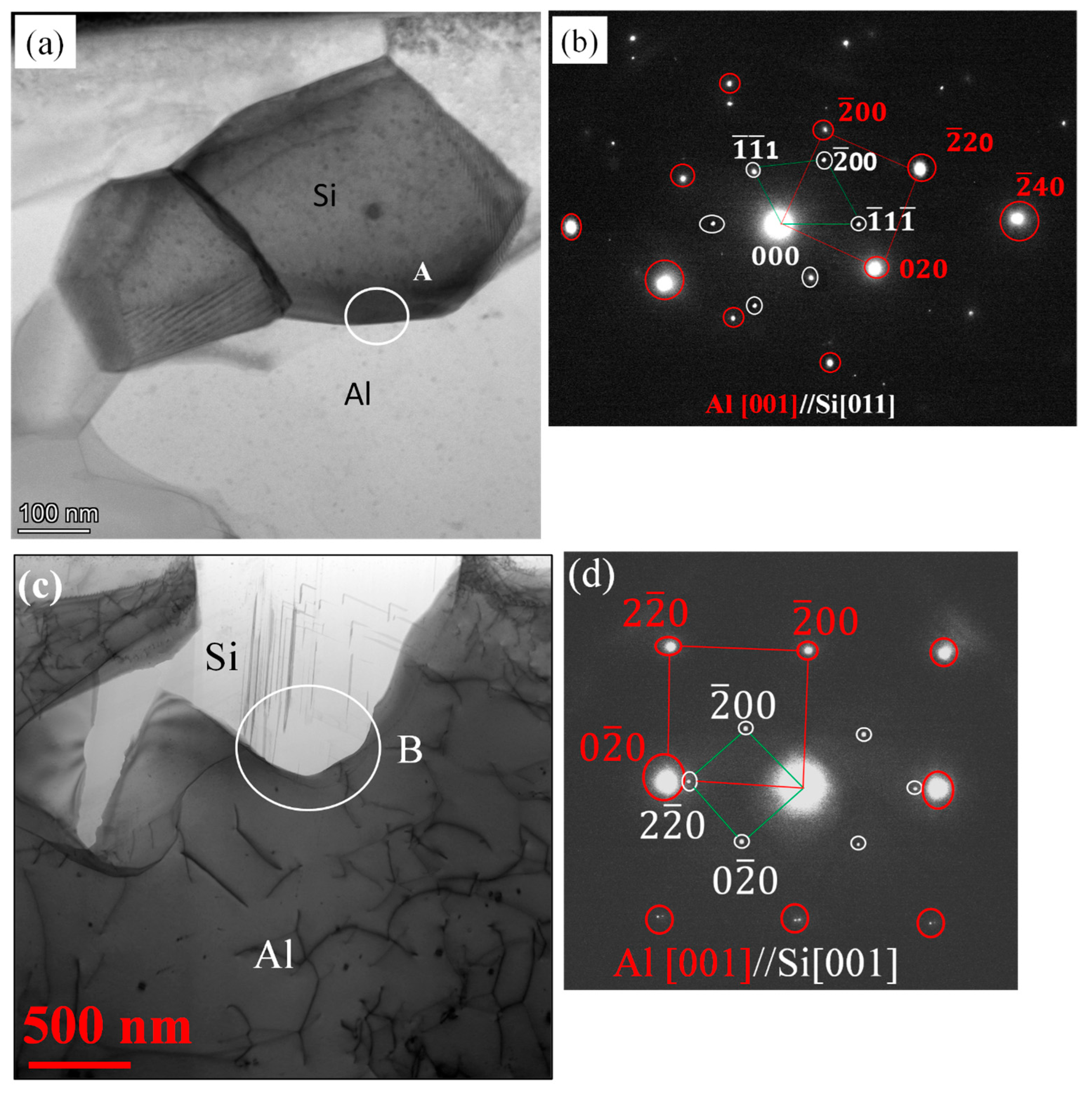
| As-cast Al-Si eutectic (Si flake) (Present study) | Al<001>//Si<011> | }Si |
| As-cast Al-Si eutectic (Si flake) [5] | Al<211>//Si<110> | {102}Al//{111}Si |
| Al<100>//Si<110> | {012}Al//{111}Si | |
| As-cast Al-Si-Sr eutectic (Si flake) (Present study) | Al<001>//Si<001> | }Si |
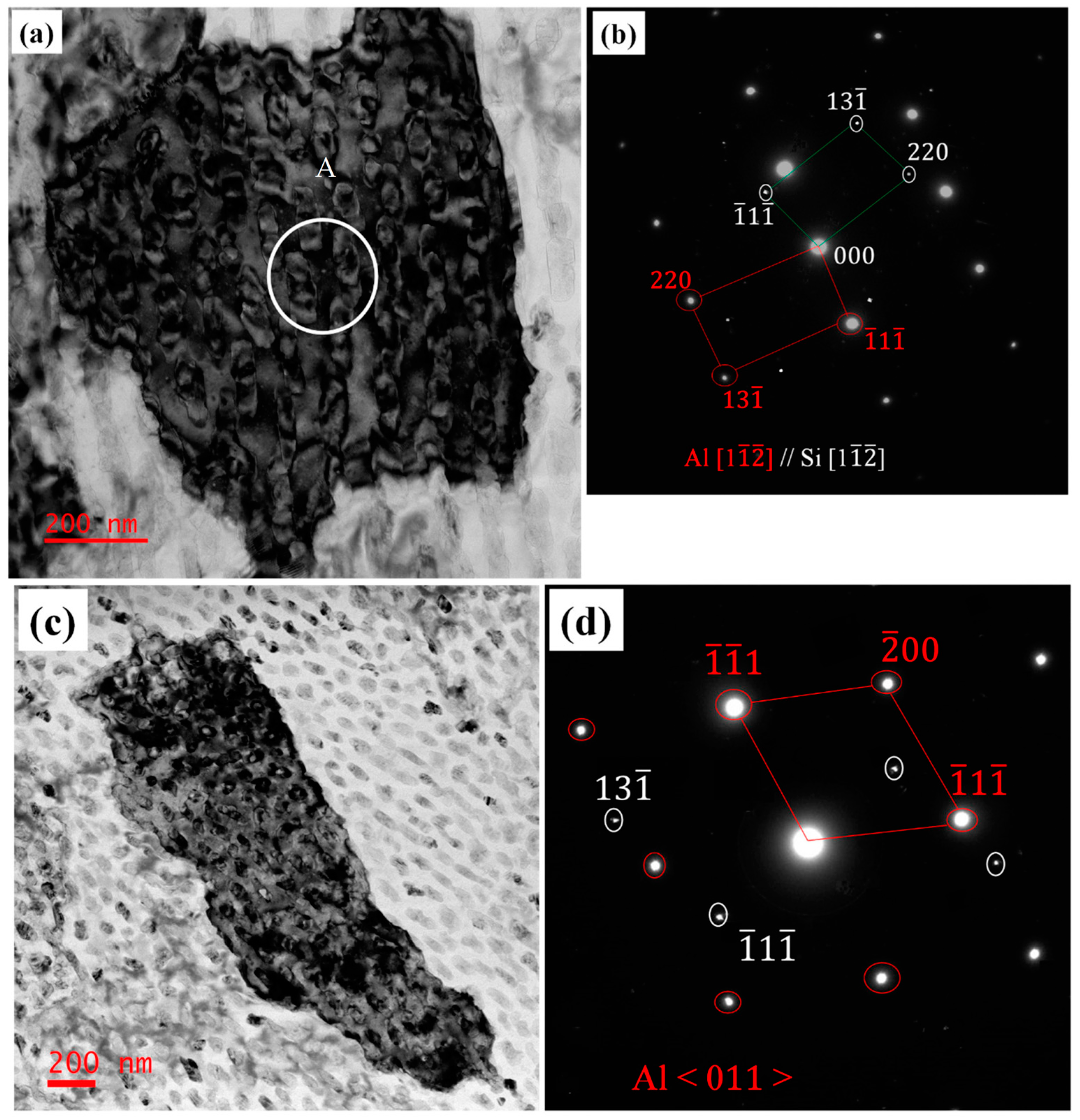
| LSR Al-20Si nanoeutectic (Si nanofibers) (Present study) | Al<111>//Si<112> | }Si |
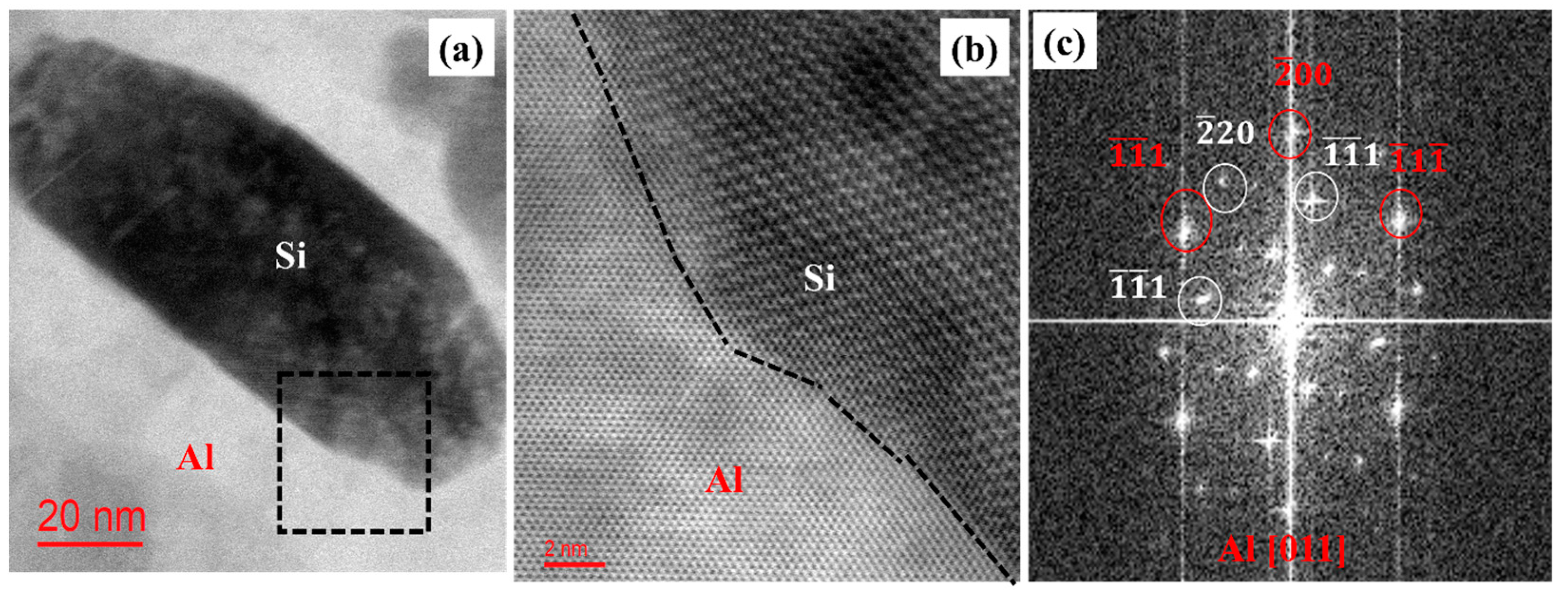
| LSR Al-20Si nanoeutectic (Si nanofibers) [24] | Al<111>Al//Si<112> | {112}Al//{111}Si |
| LSR Al-20Si-0.2Sr nanoeutectic (Si nanofibers) (Present study) | Al<112>//Si<112> | 12° mis-orientation between {113}Al and {113}Si, {111}Al and {111}Si, {220}Al and {220}Si |
| Parallel Planes | Interface Type | d-Spacings (nm) | nAl/nSi | εx/y (%) |
|---|---|---|---|---|
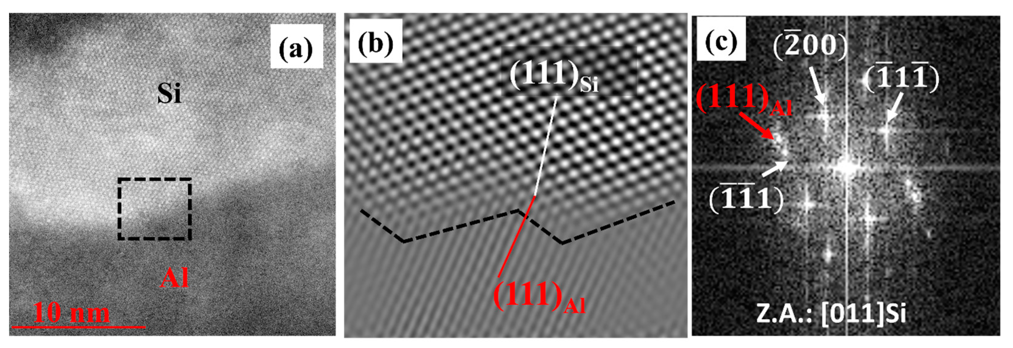
| (111)Al//(111)Si | Semi-coherent | dAl(111) = 0.2338 dSi(111) = 0.3113 | 19/14 [31] | 1.9 |
| Coherent | dAl(111) = 0.2338 dSi(111) = 0.3106 | 4/3 | 0.13 |
Disclaimer/Publisher’s Note: The statements, opinions and data contained in all publications are solely those of the individual author(s) and contributor(s) and not of MDPI and/or the editor(s). MDPI and/or the editor(s) disclaim responsibility for any injury to people or property resulting from any ideas, methods, instructions or products referred to in the content. |
© 2024 by the authors. Licensee MDPI, Basel, Switzerland. This article is an open access article distributed under the terms and conditions of the Creative Commons Attribution (CC BY) license (https://creativecommons.org/licenses/by/4.0/).
Share and Cite
Sahu, B.P.; Andani, M.T.; Ghosh, A.; Wang, J.; Misra, A. Crystallography and Interface Structures in As-Arc Melted and Laser Surface-Remelted Aluminum–Silicon Alloys with and without Strontium Addition. Crystals 2024, 14, 283. https://doi.org/10.3390/cryst14030283
Sahu BP, Andani MT, Ghosh A, Wang J, Misra A. Crystallography and Interface Structures in As-Arc Melted and Laser Surface-Remelted Aluminum–Silicon Alloys with and without Strontium Addition. Crystals. 2024; 14(3):283. https://doi.org/10.3390/cryst14030283
Chicago/Turabian StyleSahu, Bibhu P., Mohsen T. Andani, Arkajit Ghosh, Jian Wang, and Amit Misra. 2024. "Crystallography and Interface Structures in As-Arc Melted and Laser Surface-Remelted Aluminum–Silicon Alloys with and without Strontium Addition" Crystals 14, no. 3: 283. https://doi.org/10.3390/cryst14030283