
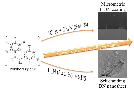
How to Increase the h-BN Crystallinity of Microfilms and Self-Standing Nanosheets: A Review of the Different Strategies Using the PDCs Route

 , ,
, , 
Abstract
:
1. Introduction
2. First strategy: Rapid Thermal Annealing (RTA)
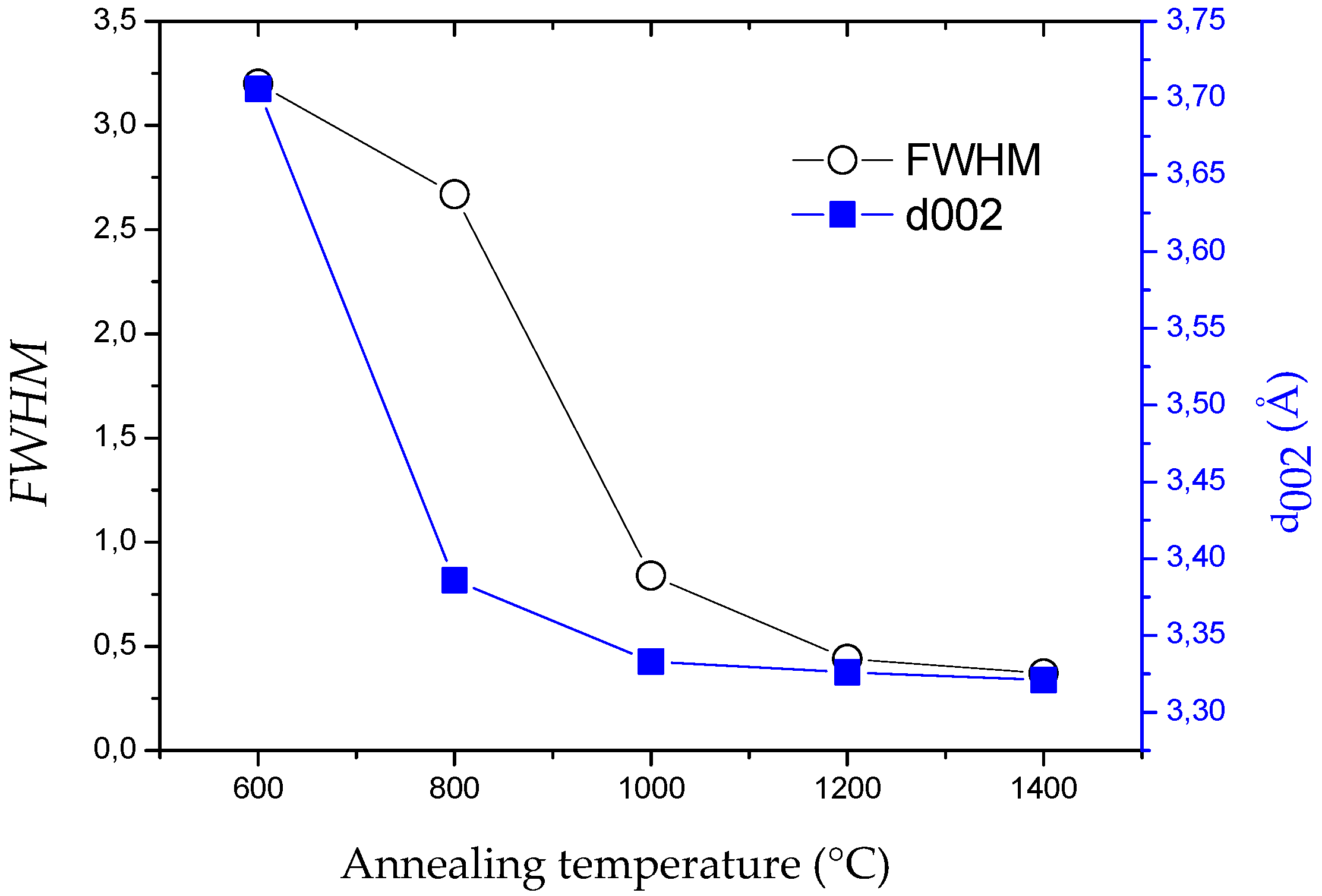
2.1. Influence of the Annealing Temperature
2.2. Influence of Annealing Process and Atmosphere (RTA)
3. Second Strategy: Li3N as Crystallization Promoter
3.1. Evidence of Li3N Effect
3.2. Influence of the Annealing Temperature on h-BN Crystallization
3.3. Thick h-BN Synthesis
3.4. BNNS Preparation
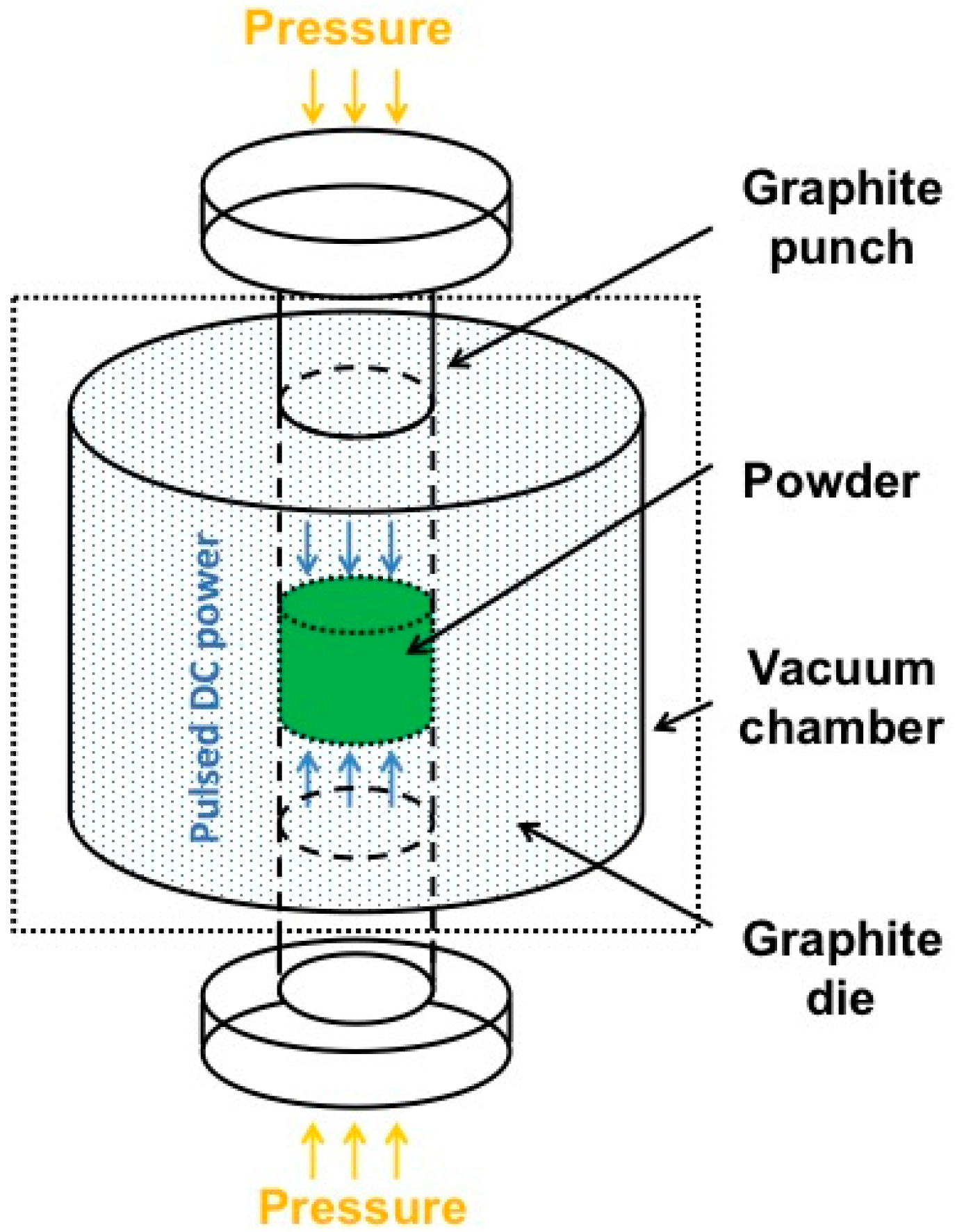
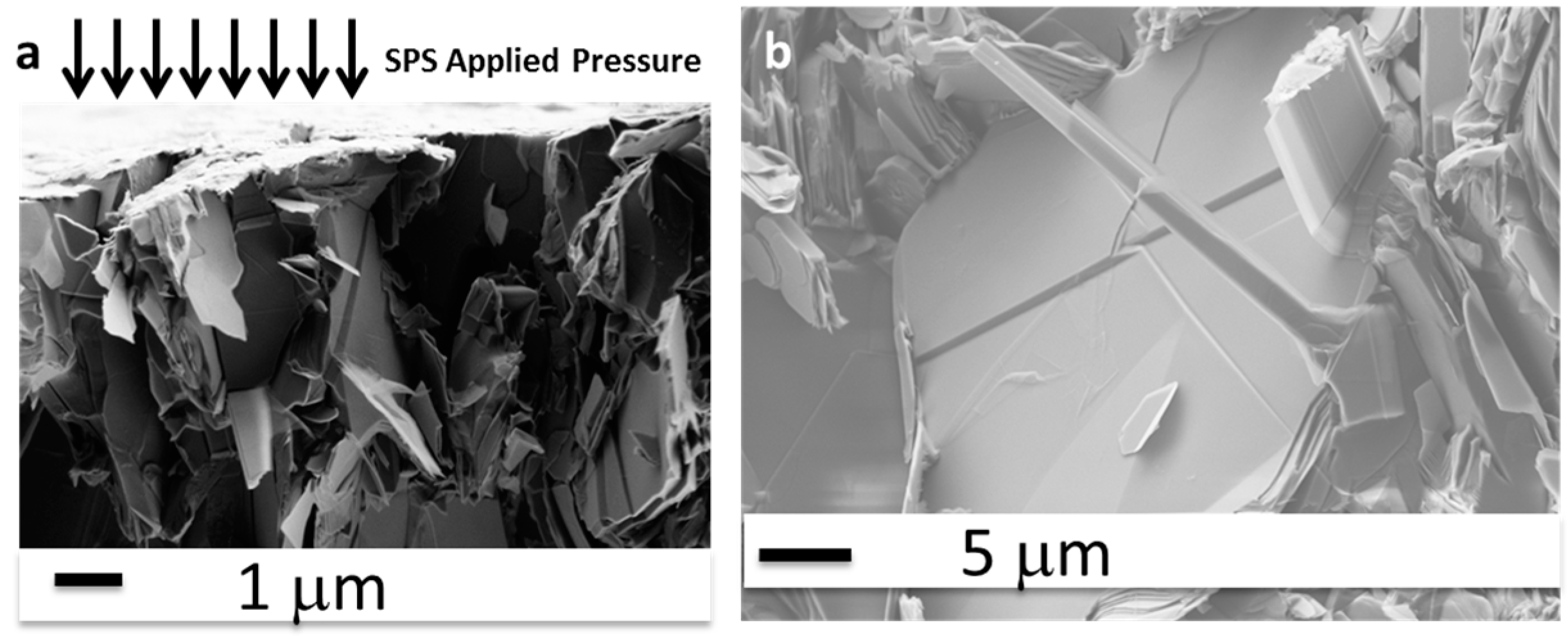
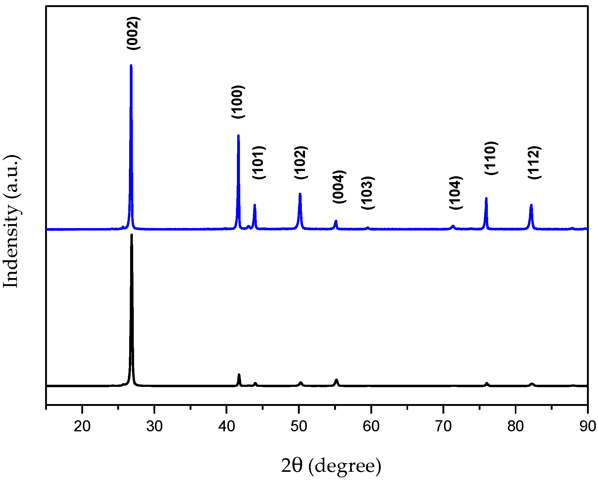
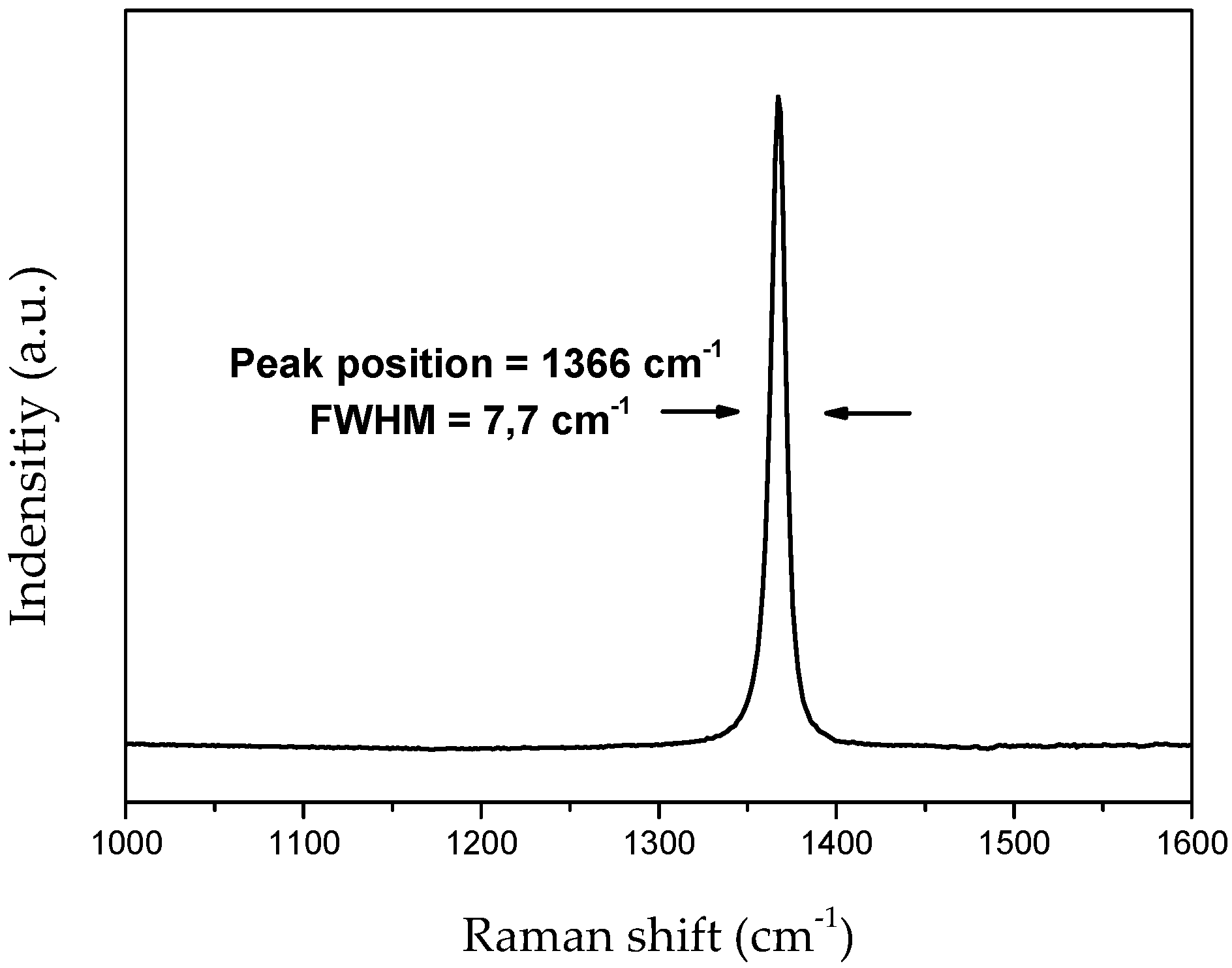
4. Third Strategy: Combining PDCs with SPS
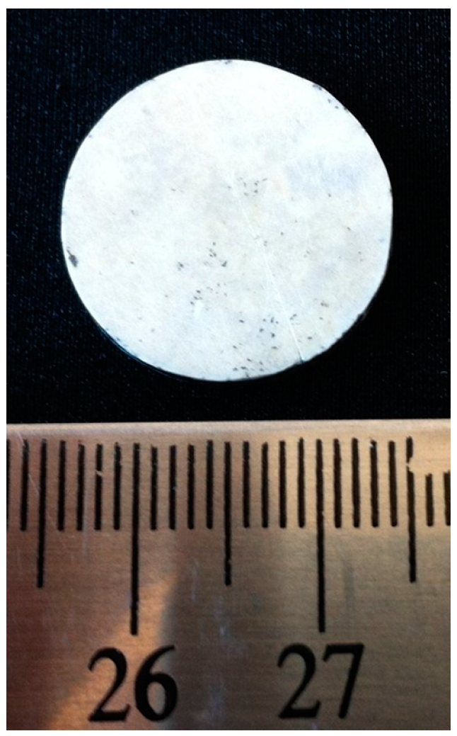
4.1. Characterization of the Bulk h-BN Pellet
4.2. Characterization of Single Crystal Flakes
4.3. Characterisation of the BNNS
5. Materials and Methods
5.1. Borazine and PBN Syntheses
5.2. Characteization Tools
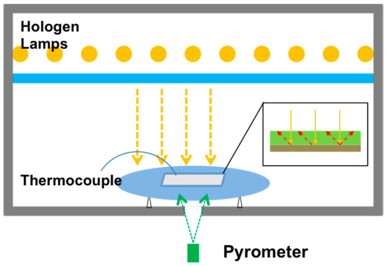
5.3. Specific Apparatus
6. Conclusions
Acknowledgments
Author Contributions
Conflicts of Interest
References
- Paine, R.T.; Narula, C.K. Synthetic routes to boron nitride. Chem. Rev. 1990, 90, 73–91. [Google Scholar] [CrossRef]
- Han, W.-Q. Anisotropic Hexagonal Boron Nitride Nanomaterials: Synthesis and Applications. In Nanotechnologies for the Life Sciences; Wiley-VCH Verlag GmbH & Co. KGaA: Weinheim, Germany, 2007. [Google Scholar]
- Jiang, X.-F.; Weng, Q.; Wang, X.-B.; Li, X.; Zhang, J.; Golberg, D.; Bando, Y. Recent Progress on Fabrications and Applications of Boron Nitride Nanomaterials: A Review. J. Mater. Sci. Technol. 2015, 31, 589–598. [Google Scholar] [CrossRef]
- Toury, B.; Miele, P. A new polyborazine-based route to boron nitride fibres. J. Mater. Chem. 2004, 14, 2609–2611. [Google Scholar] [CrossRef]
- Toury, B.; Bernard, S.; Cornu, D.; Chassagneux, F.; Létoffé, J.-M.; Miele, P. High-performance boron nitride fibers obtained from asymmetric alkylaminoborazine. J. Mater. Chem. 2003, 13, 274–279. [Google Scholar] [CrossRef]
- Toury, B.; Miele, P.; Cornu, D.; Vincent, H.; Bouix, J. Boron Nitride Fibers Prepared from Symmetric and Asymmetric Alkylaminoborazines. Adv. Funct. Mater. 2002, 12, 228–234. [Google Scholar] [CrossRef]
- Miele, P.; Bernard, S.; Cornu, D.; Toury, B. Recent Developments in Polymer-Derived Ceramic Fibers (PDCFs): Preparation, Properties and Applications—A Review. Soft Mater. 2007, 4, 249–286. [Google Scholar] [CrossRef]
- Bernard, S.; Ayadi, K.; Berthet, M.-P.; Chassagneux, F.; Cornu, D.; Letoffe, J.-M.; Miele, P. Evolution of structural features and mechanical properties during the conversion of poly[(methylamino)borazine] fibers into boron nitride fibers. J. Solid State Chem. 2004, 177, 1803–1810. [Google Scholar] [CrossRef]
- Kalay, S.; Yilmaz, Z.; Sen, O.; Emanet, M.; Kazanc, E.; Çulha, M. Synthesis of boron nitride nanotubes and their applications. Beilstein J. Nanotechnol. 2015, 6, 84–102. [Google Scholar] [CrossRef] [PubMed]
- Tiano, A.L.; Park, C.; Lee, J.W.; Luong, H.H.; Gibbons, L.J.; Chu, S.-H.; Applin, S.; Gnoffo, P.; Lowther, S.; Kim, H.J.; et al. Boron nitride nanotube: Synthesis and applications. Proc. SPIE 2014, 9060. [Google Scholar] [CrossRef]
- Wang, J.; Lee, C.H.; Bando, Y.; Golberg, D.; Yap, Y.K. Multiwalled Boron Nitride Nanotubes: Growth, Properties, and Applications. In B-C-N Nanotubes and Related Nanostructures; Springer New York: New York, NY, USA, 2009; pp. 23–44. [Google Scholar]
- Stéphan, O.; Bando, Y.; Loiseau, A.; Willaime, F.; Shramchenko, N.; Tamiya, T.; Sato, T. Formation of small single-layer and nested BN cages under electron irradiation of nanotubes and bulk material. Appl. Phys. A 1998, 67, 107–111. [Google Scholar] [CrossRef]
- Golberg, D.; Bando, Y.; Stéphan, O.; Kurashima, K. Octahedral boron nitride fullerenes formed by electron beam irradiation. Appl. Phys. Lett. 1998, 73, 2441–2443. [Google Scholar] [CrossRef]
- Lin, Y.; Connell, J.W. Advances in 2D boron nitride nanostructures: Nanosheets, nanoribbons, nanomeshes, and hybrids with graphene. Nanoscale 2012, 4, 6908. [Google Scholar] [CrossRef] [PubMed]
- Arenal, R.; Lopez-Bezanilla, A. Boron nitride materials: An overview from 0D to 3D (nano)structures. Wiley Interdiscip. Rev. Comput. Mol. Sci. 2015, 5, 299–309. [Google Scholar] [CrossRef]
- Haubner, R.; Wilhelm, M.; Weissenbacher, R.; Lux, B. Boron Nitrides—Properties, Synthesis and Applications; Springer Berlin Heidelberg: Berlin, Germany; Heidelberg, Germany, 2002. [Google Scholar]
- Clere, T.M. Method for Making High Thermal Diffusivity Boron Nitride Powders. Google Patents U.S. 6764975 B1, 20 July 2004. [Google Scholar]
- Lin, K.Y.; Raman, C.; Xiang, B.; Murugaiah, A. Composition comprising exfoliated boron nitride and method for forming such compositions; Google Patents US 20140077125 A1, 20 March 2014. [Google Scholar]
- Chantrell, P.G.; Popper, P. Inorganic Polymers for Ceramics; Special Ceramics; Academic Press; Popper: New York, NY, USA, 1965; Volume 4. [Google Scholar]
- Colombo, P.; Mera, G.; Riedel, R.; Sorarù, G.D. Polymer-Derived Ceramics: 40 Years of Research and Innovation in Advanced Ceramics: Polymer-Derived Ceramics. J. Am. Ceram. Soc. 2010, 93, 1805–1837. [Google Scholar] [CrossRef]
- Bernard, S.; Salameh, C.; Miele, P. Boron nitride ceramics from molecular precursors: Synthesis, properties and applications. Dalton Trans. 2016, 45, 861–873. [Google Scholar] [CrossRef] [PubMed]
- Rice, R. Ceramics from polymer pyrolysis, opportunities and needs—A materials perspective. Am. Ceram. Soc. Bull. 1983, 62, 889–892. [Google Scholar]
- Walker, B.; Rice, R.; Becher, P.; Bender, B.; Coblenz, W. Preparation and properties of monolithic and composite ceramics produced by polymer pyrolysis. Am. Ceram. Soc. Bull. 1983, 62, 916–923. [Google Scholar]
- Wynne, K.J.; Rice, R.W. Ceramics Via Polymer Pyrolysis dagger. Annu. Rev. Mater. Sci. 1984, 14, 297–334. [Google Scholar] [CrossRef]
- Bernard, S.; Miele, P. Polymer-Derived Boron Nitride: A Review on the Chemistry, Shaping and Ceramic Conversion of Borazine Derivatives. Materials 2014, 7, 7436–7459. [Google Scholar] [CrossRef]
- Kusari, U.; Bao, Z.; Cai, Y.; Ahmad, G.; Sandhage, K.H.; Sneddon, L.G. Formation of nanostructured, nanocrystalline boron nitride microparticles with diatom-derived 3-D shapes. Chem. Commun. 2007, 1177–1179. [Google Scholar] [CrossRef] [PubMed]
- Zhong, W.; Wang, S.; Li, J.; Bechelany, M.C.; Ghisleni, R.; Rossignol, F.; Balan, C.; Chartier, T.; Bernard, S.; Miele, P. Design of carbon fiber reinforced boron nitride matrix composites by vacuum-assisted polyborazylene transfer molding and pyrolysis. J. Eur. Ceram. Soc. 2013, 33, 2979–2992. [Google Scholar] [CrossRef]
- Li, J.; Bernard, S.; Salles, V.; Gervais, C.; Miele, P. Preparation of Polyborazylene-Derived Bulk Boron Nitride with Tunable Properties by Warm-Pressing and Pressureless Pyrolysis. Chem. Mater. 2010, 22, 2010–2019. [Google Scholar] [CrossRef]
- Alauzun, J.G.; Ungureanu, S.; Brun, N.; Bernard, S.; Miele, P.; Backov, R.; Sanchez, C. Novel monolith-type boron nitride hierarchical foams obtained through integrative chemistry. J. Mater. Chem. 2011, 21, 14025–14030. [Google Scholar] [CrossRef]
- Termoss, H.; Toury, B.; Brioude, A.; Dazord, J.; Le Brusq, J.; Miele, P. High purity boron nitride thin films prepared by the PDCs route. Surf. Coat. Technol. 2007, 201, 7822–7828. [Google Scholar] [CrossRef]
- Yuan, S.; Toury, B.; Benayoun, S. Novel chemical process for preparing h-BN solid lubricant coatings on titanium-based substrates for high temperature tribological applications. Surf. Coat. Technol. 2015, 272, 366–372. [Google Scholar] [CrossRef]
- Termoss, H.; Toury, B.; Pavan, S.; Brioude, A.; Bernard, S.; Cornu, D.; Valette, S.; Benayoun, S.; Miele, P. Preparation of boron nitride-based coatings on metallic substrates via infrared irradiation of dip-coated polyborazylene. J. Mater. Chem. 2009, 19, 2671–2674. [Google Scholar] [CrossRef]
- Yuan, S.; Benayoun, S.; Brioude, A.; Dezellus, O.; Beaugiraud, B.; Toury, B. New potential for preparation of performing h-BN coatings via polymer pyrolysis in RTA furnace. J. Eur. Ceram. Soc. 2013, 33, 393–402. [Google Scholar] [CrossRef]
- Lattemann, M.; Sell, K.; Ye, J.; Persson, P.Å.O.; Ulrich, S. Stress reduction in nanocomposite coatings consisting of hexagonal and cubic boron nitride. Thin Films 2006, 200, 6459–6464. [Google Scholar] [CrossRef]
- Mitu, B.; Bilkova, P.; Marotta, V.; Orlando, S.; Santagata, A. RF plasma reactive pulsed laser deposition of boron nitride thin films. Appl. Surf. Sci. 2005, 247, 123–127. [Google Scholar] [CrossRef]
- Mroz, W.; Kosydar, R.; Jelinek, M.; Kocourek, T.; Major, B. Phase formation and microstructure of boron nitride thin layers deposited using Nd:YAG and KrF lasers. Thin Films 2006, 200, 6438–6443. [Google Scholar] [CrossRef]
- Greber, T.; Brandenberger, L.; Corso, M.; Tamai, A.; Osterwalder, J. Single layer hexagonal boron nitride films on Ni(110). E-J. Surf. Sci. Nanotechnol. 2006, 4, 410–413. [Google Scholar] [CrossRef]
- Ćavar, E.; Westerström, R.; Mikkelsen, A.; Lundgren, E.; Vinogradov, A.S.; Ng, M.L.; Preobrajenski, A.B.; Zakharov, A.A.; Mårtensson, N. A single h-BN layer on Pt(1 1 1). Surf. Sci. 2008, 602, 1722–1726. [Google Scholar] [CrossRef]
- Le Gallet, S.; Chollon, G.; Rebillat, F.; Guette, A.; Bourrat, X.; Naslain, R.; Couzi, M.; Bruneel, J. Microstructural and microtextural investigations of boron nitride deposited from BCl3–NH3–H2 gas mixtures. J. Eur. Ceram. Soc. 2004, 24, 33–44. [Google Scholar] [CrossRef]
- Deb, B.; Bhattacharjee, B.; Ganguli, A.; Chaudhuri, S.; Pal, A.K. Boron nitride films synthesized by RF plasma CVD of borane–ammonia and nitrogen. Mater. Chem. Phys. 2002, 76, 130–136. [Google Scholar] [CrossRef]
- Dekempeneer, E.H.A.; Kuypers, S.; Vercammen, K.; Meneve, J.; Smeets, J.; Gibson, P.N.; Gissler, W. Scratch-resistant transparent boron nitride films. Surf. Coat. Technol. 1998, 100–101, 45–48. [Google Scholar] [CrossRef]
- Soltani, A.; Thévenin, P.; Bath, A. Optical properties of boron nitride thin films deposited by microwave PECVD. Mater. Sci. Eng. B 2001, 82, 170–172. [Google Scholar] [CrossRef]
- Yuan, S. Elaboration de Revêtements de Nitrure (h-BN et SI3N4) par Pyrolyse de Polymere Précéramique: Caractérisations Chimiques, Structurales, Mécaniques et Tribologiques. Ph.D. Thesis, Ecole Centrale de Lyon, Ecully, France, 2013. [Google Scholar]
- Middleman, S. The role of gas-phase reactions in boron nitride growth by chemical vapor deposition. Mater. Sci. Eng. A 1993, 163, 135–140. [Google Scholar] [CrossRef]
- Kho, J.-G.; Moon, K.-T.; Nouet, G.; Ruterana, P.; Kim, D.-P. Boron-rich boron nitride (BN) films prepared by a single spin-coating process of a polymeric precursor. Thin Solid Films 2001, 389, 78–83. [Google Scholar] [CrossRef]
- Design, Processing, and Properties of Ceramic Materials from Preceramic Precursors. In Materials Science and Technologies; Bernard, S. (Ed.) Nova Science Publishers: New York, NY, USA, 2012.
- Beck, J.S.; Albani, C.R.; McGhie, A.R.; Rothman, J.B.; Sneddon, L.G. Dibromoborane-dimethyl sulfide: A simple molecular precursor for the formation of bulk powders and fiber coatings of boron nitride. Chem. Mater. 1989, 1, 433–438. [Google Scholar] [CrossRef]
- Bonnetot, B.; Guilhon, F.; Viala, J.C.; Mongeot, H. Boron Nitride Matrixes and Coatings Obtained from Tris(methylamino)borane. Application to the Protection of Graphite against Oxidation. Chem. Mater. 1995, 7, 299–303. [Google Scholar] [CrossRef]
- Thévenot, F.; Doche, C.; Mongeot, H.; Guilhon, F.; Miele, P.; Cornu, D.; Bonnetot, B. Boron Nitride Obtained from Molecular Precursors: Aminoboranes Used as a BN Source for Coatings, Matrix, and Si3N4–BN Composite Ceramic Preparation. J. Solid State Chem. 1997, 133, 164–168. [Google Scholar] [CrossRef]
- Cornu, D.; Miele, P.; Toury, B.; Bonnetot, B.; Mongeot, H.; Bouix, J. Boron nitride matrices and coatings from boryl borazine molecular precursors. J. Mater. Chem. 1999, 9, 2605–2610. [Google Scholar] [CrossRef]
- Borek, T.T.; Qiu, X.; Rayfuse, L.M.; Datye, A.K.; Paine, R.T.; Allard, L.F. Boron Nitride Coatings on Oxide Substrates: Role of Surface Modifications. J. Am. Ceram. Soc. 1991, 74, 2587–2591. [Google Scholar] [CrossRef]
- Paciorek, K.J.L.; Masuda, S.R.; Kratzer, R.H.; Schmidt, W.R. Processible precursor for boron nitride coatings and matrixes. Chem. Mater. 1991, 3, 88–91. [Google Scholar] [CrossRef]
- Kim, D.P.; Economy, J. Fabrication of oxidation-resistant carbon fiber/boron nitride matrix composites. Chem. Mater. 1993, 5, 1216–1220. [Google Scholar] [CrossRef]
- Cavallo, F.; Rojas Delgado, R.; Kelly, M.M.; Sánchez Pérez, J.R.; Schroeder, D.P.; Xing, H.G.; Eriksson, M.A.; Lagally, M.G. Exceptional Charge Transport Properties of Graphene on Germanium. ACS Nano 2014, 8, 10237–10245. [Google Scholar] [CrossRef] [PubMed]
- Dean, C.R.; Young, A.F.; Meric, I.; Lee, C.; Wang, L.; Sorgenfrei, S.; Watanabe, K.; Taniguchi, T.; Kim, P.; Shepard, K.L.; Hone, J. Boron nitride substrates for high-quality graphene electronics. Nat. Nanotechnol. 2010, 5, 722–726. [Google Scholar] [CrossRef] [PubMed]
- Gannett, W.; Regan, W.; Watanabe, K.; Taniguchi, T.; Crommie, M.F.; Zettl, A. Boron nitride substrates for high mobility chemical vapor deposited graphene. Appl. Phys. Lett. 2011, 98, 242105. [Google Scholar] [CrossRef]
- Lee, G.-H.; Yu, Y.-J.; Lee, C.; Dean, C.; Shepard, K.L.; Kim, P.; Hone, J. Electron tunneling through atomically flat and ultrathin hexagonal boron nitride. Appl. Phys. Lett. 2011, 99, 243114. [Google Scholar] [CrossRef]
- Golberg, D.; Bando, Y.; Huang, Y.; Terao, T.; Mitome, M.; Tang, C.; Zhi, C. Boron Nitride Nanotubes and Nanosheets. ACS Nano 2010, 4, 2979–2993. [Google Scholar] [CrossRef] [PubMed]
- Decker, R.; Wang, Y.; Brar, V.W.; Regan, W.; Tsai, H.-Z.; Wu, Q.; Gannett, W.; Zettl, A.; Crommie, M.F. Local Electronic Properties of Graphene on a BN Substrate via Scanning Tunneling Microscopy. Nano Lett. 2011, 11, 2291–2295. [Google Scholar] [CrossRef] [PubMed]
- Xue, J.; Sanchez-Yamagishi, J.; Bulmash, D.; Jacquod, P.; Deshpande, A.; Watanabe, K.; Taniguchi, T.; Jarillo-Herrero, P.; LeRoy, B.J. Scanning tunnelling microscopy and spectroscopy of ultra-flat graphene on hexagonal boron nitride. Nat. Mater. 2011, 10, 282–285. [Google Scholar] [CrossRef] [PubMed]
- Song, L.; Ci, L.; Lu, H.; Sorokin, P.B.; Jin, C.; Ni, J.; Kvashnin, A.G.; Kvashnin, D.G.; Lou, J.; Yakobson, B.I.; et al. Large scale growth and characterization of atomic hexagonal boron nitride layers. Nano Lett. 2010, 10, 3209–3215. [Google Scholar] [CrossRef] [PubMed]
- Shi, Y.; Hamsen, C.; Jia, X.; Kim, K.K.; Reina, A.; Hofmann, M.; Hsu, A.L.; Zhang, K.; Li, H.; Juang, Z.-Y.; et al. Synthesis of Few-Layer Hexagonal Boron Nitride Thin Film by Chemical Vapor Deposition. Nano Lett. 2010, 10, 4134–4139. [Google Scholar] [CrossRef] [PubMed]
- Zhang, C.; Fu, L.; Zhao, S.; Zhou, Y.; Peng, H.; Liu, Z. Controllable Co-segregation Synthesis of Wafer-Scale Hexagonal Boron Nitride Thin Films. Adv. Mater. 2014, 26, 1776–1781. [Google Scholar] [CrossRef] [PubMed]
- Gao, Y.; Ren, W.; Ma, T.; Liu, Z.; Zhang, Y.; Liu, W.-B.; Ma, L.-P.; Ma, X.; Cheng, H.-M. Repeated and Controlled Growth of Monolayer, Bilayer and Few-Layer Hexagonal Boron Nitride on Pt Foils. ACS Nano 2013, 7, 5199–5206. [Google Scholar] [CrossRef] [PubMed]
- Lu, G.; Wu, T.; Yuan, Q.; Wang, H.; Wang, H.; Ding, F.; Xie, X.; Jiang, M. Synthesis of large single-crystal hexagonal boron nitride grains on Cu–Ni alloy. Nat. Commun. 2015, 6. [Google Scholar] [CrossRef] [PubMed]
- Caneva, S.; Weatherup, R.S.; Bayer, B.C.; Brennan, B.; Spencer, S.J.; Mingard, K.; Cabrero-Vilatela, A.; Baehtz, C.; Pollard, A.J.; Hofmann, S. Nucleation Control for Large, Single Crystalline Domains of Monolayer Hexagonal Boron Nitride via Si-Doped Fe Catalysts. Nano Lett. 2015, 15, 1867–1875. [Google Scholar] [CrossRef] [PubMed]
- Park, J.-H.; Park, J.C.; Yun, S.J.; Kim, H.; Luong, D.H.; Kim, S.M.; Choi, S.H.; Yang, W.; Kong, J.; Kim, K.K.; et al. Large-Area Monolayer Hexagonal Boron Nitride on Pt Foil. ACS Nano 2014, 8, 8520–8528. [Google Scholar] [CrossRef] [PubMed]
- Camilli, L.; Sutter, E.; Sutter, P. Growth of two-dimensional materials on non-catalytic substrates: H-BN/Au(111). 2D Mater. 2014, 1, 025003. [Google Scholar] [CrossRef]
- Corso, M.; Auwärter, W.; Muntwiler, M.; Tamai, A.; Greber, T.; Osterwalder, J. Boron Nitride Nanomesh. Science 2004, 303, 217–220. [Google Scholar] [CrossRef] [PubMed]
- Simonson, R.J.; Paffett, M.T.; Jones, M.E.; Koel, B.E. A vibrational study of borazine adsorbed on Pt(111) and Au(111) surfaces. Surf. Sci. 1991, 254, 29–44. [Google Scholar] [CrossRef]
- Preobrajenski, A.B.; Nesterov, M.A.; Ng, M.L.; Vinogradov, A.S.; Mårtensson, N. Monolayer h-BN on lattice-mismatched metal surfaces: On the formation of the nanomesh. Chem. Phys. Lett. 2007, 446, 119–123. [Google Scholar] [CrossRef]
- Sutter, P.; Lahiri, J.; Albrecht, P.; Sutter, E. Chemical Vapor Deposition and Etching of High-Quality Monolayer Hexagonal Boron Nitride Films. ACS Nano 2011, 5, 7303–7309. [Google Scholar] [CrossRef] [PubMed]
- Kim, K.K.; Hsu, A.; Jia, X.; Kim, S.M.; Shi, Y.; Hofmann, M.; Nezich, D.; Rodriguez-Nieva, J.F.; Dresselhaus, M.; Palacios, T.; et al. Synthesis of Monolayer Hexagonal Boron Nitride on Cu Foil Using Chemical Vapor Deposition. Nano Lett. 2012, 12, 161–166. [Google Scholar] [CrossRef] [PubMed]
- Tay, R.Y.; Griep, M.H.; Mallick, G.; Tsang, S.H.; Singh, R.S.; Tumlin, T.; Teo, E.H. T.; Karna, S.P. Growth of Large Single-Crystalline Two-Dimensional Boron Nitride Hexagons on Electropolished Copper. Nano Lett. 2014, 14, 839–846. [Google Scholar] [CrossRef] [PubMed]
- Wang, L.; Wu, B.; Chen, J.; Liu, H.; Hu, P.; Liu, Y. Monolayer Hexagonal Boron Nitride Films with Large Domain Size and Clean Interface for Enhancing the Mobility of Graphene-Based Field-Effect Transistors. Adv. Mater. 2014, 26, 1559–1564. [Google Scholar] [CrossRef] [PubMed]
- Yuan, S.; Linas, S.; Journet, C.; Steyer, P.; Garnier, V.; Bonnefont, G.; Brioude, A.; Toury, B. Pure & crystallized 2D Boron Nitride sheets synthesized via a novel process coupling both PDCs and SPS methods. Sci. Rep. 2016, 6, 20388. [Google Scholar] [PubMed]
- Watanabe, K.; Taniguchi, T.; Kanda, H. Direct-bandgap properties and evidence for ultraviolet lasing of hexagonal boron nitride single crystal. Nat. Mater. 2004, 3, 404–409. [Google Scholar] [CrossRef] [PubMed]
- Kubota, Y.; Watanabe, K.; Tsuda, O.; Taniguchi, T. Deep Ultraviolet Light-Emitting Hexagonal Boron Nitride Synthesized at Atmospheric Pressure. Science 2007, 317, 932–934. [Google Scholar] [CrossRef] [PubMed]
- Termoss, H. Préparation de Revêtements de Nitrure de Bore (BN) par voie Polymère Précéramique: Etude Des Paramètres d’élaboration: Caractérisations Physico-Chimiques, Ph.D. Thesis, Université Claude Bernard-Lyon I, Villeurbanne, France, 2009. [Google Scholar]
- Kho, J.-G.; Moon, K.-T.; Kim, J.-H.; Kim, D.-P. Properties of Boron Nitride (BxNy) Films Produced by the Spin-Coating Process of Polyborazine. J. Am. Ceram. Soc. 2000, 83, 2681–2683. [Google Scholar] [CrossRef]
- Chan, V.Z.-H.; Rothman, J.B.; Palladino, P.; Sneddon, L.G.; Composto, R.J. Characterization of boron nitride thin films prepared from a polymer precursor. J. Mater. Res. 1996, 11, 373–380. [Google Scholar] [CrossRef]
- Vilcarromero, J.; Carreño, M.N.; Pereyra, I. Mechanical properties of boron nitride thin films obtained by RF-PECVD at low temperatures. Thin Solid Films 2000, 373, 273–276. [Google Scholar] [CrossRef]
- Nemanich, R.J.; Solin, S.A.; Martin, R.M. Light scattering study of boron nitride microcrystals. Phys. Rev. B 1981, 23, 6348–6356. [Google Scholar] [CrossRef]
- Mera, G. Polymer Derived-Ceramic MicroElectroMechanical Systems (PDC-MEMS). In Design, Processing and Properties of Ceramic Materials from Preceramic Precursors. Materials Science and Technologies; Bernard, S., Ed.; Nova Science Publisher: New York, NY, USA, 2011. [Google Scholar]
- Gervais, C.; Maquet, J.; Babonneau, F.; Duriez, C.; Framery, E.; Vaultier, M.; Florian, P.; Massiot, D. Chemically Derived BN Ceramics: Extensive 11B and 15N Solid-State NMR Study of a Preceramic Polyborazilene. Chem. Mater. 2001, 13, 1700–1707. [Google Scholar] [CrossRef]
- Fazen, P.J.; Beck, J.S.; Lynch, A.T.; Remsen, E.E.; Sneddon, L.G. Thermally induced borazine dehydropolymerization reactions. Synthesis and ceramic conversion reactions of a new high-yield polymeric precursor to boron nitride. Chem. Mater. 1990, 2, 96–97. [Google Scholar] [CrossRef]
- Sneddon, L.G.; Mirabelli, M.G.L.; Lynch, A.T.; Fazen, P.J.; Su, K.; Beck, J.S. Polymeric precursors to boron based ceramics. Pure Appl. Chem. 2009, 63, 407–410. [Google Scholar] [CrossRef]
- Fazen, P.J.; Remsen, E.E.; Beck, J.S.; Carroll, P.J.; McGhie, A.R.; Sneddon, L.G. Synthesis, Properties, and Ceramic Conversion Reactions of Polyborazylene. A High-Yield Polymeric Precursor to Boron Nitride. Chem. Mater. 1995, 7, 1942–1956. [Google Scholar] [CrossRef]
- Watanabe, K.; Taniguchi, T.; Kanda, H. Ultraviolet luminescence spectra of boron nitride single crystals grown under high pressure and high temperature. Phys. Status Solidi A 2004, 201, 2561–2565. [Google Scholar] [CrossRef]
- Solozhenko, V.L.; Turkevich, V.Z. Kinetics of cBN crystallization in the Li3N-BN system at 6.6 GPa. Diam. Relat. Mater. 1998, 7, 43–46. [Google Scholar] [CrossRef]
- Shipilo, V.B.; Ignatenko, O.V.; Shempel, N.A.; Azarko, I.I.; Lebedev, S.A. Crystallization of cubic boron nitride in the system Li3N-BN (4–10 wt % Li3N). Inorg. Mater. 2011, 44, 258–262. [Google Scholar] [CrossRef]
- Guo, X.-F.; Xu, B.; Zhang, W.; Lv, M.-Z.; Yang, H.-M.; Fan, X.-H. Thermodynamic Analysis about Nucleation and Growth of Cubic Boron Nitride Crystals in the hBN-Li3N System under High Pressure and High Temperature. Entropy 2015, 17, 755–762. [Google Scholar] [CrossRef]
- Von der Gönna, J.; Meurer, H.J.; Nover, G.; Peun, T.; Schönbohm, D.; Will, G. In-situ investigations of the reversible hBN-cBN-hBN-transformation in the Li3N-BN catalyst system using synchrotron radiation. Mater. Lett. 1998, 33, 321–326. [Google Scholar] [CrossRef]
- Du, Y.; Su, Z.; Yang, D.; Yang, X.; Ji, X.; Gong, X.; Zhang, T. Synthesis of black cBN single crystal in hBN–Li3N–B system. Mater. Lett. 2007, 61, 3409–3412. [Google Scholar] [CrossRef]
- Sheng Yuan, B.T. Low-Temperature Synthesis of Highly Crystallized Hexagonal Boron Nitride Sheets with Li3N as Additive Agent. Eur. J. Inorg. Chem. 2014, 2014. [Google Scholar] [CrossRef]
- Solozhenko, V.L.; Turkevich, V.Z. High pressure phase equilibria in the Li3N-BN system: In situ studies. Mater. Lett. 1997, 32, 179–184. [Google Scholar] [CrossRef]
- Yamane, H.; Kikkawa, S.; Koizumi, M. High- and low-temperature phases of lithium boron nitride, Li3BN2: Preparation, phase relation, crystal structure, and ionic conductivity. J. Solid State Chem. 1987, 71, 1–11. [Google Scholar] [CrossRef]
- Jacobson, N.; Farmer, S.; Moore, A.; Sayir, H. High-Temperature Oxidation of Boron Nitride: I, Monolithic Boron Nitride. J. Am. Ceram. Soc. 1999, 82, 393–398. [Google Scholar] [CrossRef]
- Vincent, H.; Chassagneux, F.; Vincent, C.; Bonnetot, B.; Berthet, M.; Vuillermoz, A.; Bouix, J. Microtexture and structure of boron nitride fibres by transmission electron microscopy, X-ray diffraction, photoelectron spectroscopy and Raman scattering. Mater. Sci. Eng. A 2003, 340, 181–192. [Google Scholar] [CrossRef]
- Bezrukov, G.; Butuzov, V.; Nikitina, T.; Feldgun, L.; Filonenk, N.E.; Khatelishvili, G.V. On crystallization of cubic boron nitride and of synthetic diamond. Dokl. Akad. NAUK SSSR 1968, 179, 1326. [Google Scholar]
- Li, S.; Guo, X.; Xu, B.; Wang, H. Fracture morphology and XRD layered characterization of cBN cake. J. Synth. Cryst. 2012, 41, 15–19. [Google Scholar]
- Xu, B.; Lv, M.-Z.; Yang, H.-M.; Wen, Z.-X. Thermodynamic Analysis of the V-Shaped Area of High Pressure and High Temperature in Cubic Boron Nitride Synthesis with Li3N as a Catalyst. Entropy 2014, 16, 912–920. [Google Scholar] [CrossRef]
- Yuan, S.; Toury, B.; Journet, C.; Brioude, A. Synthesis of hexagonal boron nitride graphene-like few layers. Nanoscale 2014, 6, 7838–7841. [Google Scholar] [CrossRef] [PubMed]
- Xu, L.Q.; Zhan, J.H.; Hu, J.Q.; Bando, Y.; Yuan, X.L.; Sekiguchi, T.; Mitome, M.; Golberg, D. High-Yield Synthesis of Rhombohedral Boron Nitride Triangular Nanoplates. Adv. Mater. 2007, 19, 2141–2144. [Google Scholar] [CrossRef]
- Sediri, H.; Pierucci, D.; Hajlaoui, M.; Henck, H.; Patriarche, G.; Dappe, Y.J.; Yuan, S.; Toury, B.; Belkhou, R.; Silly, M.G.; et al. Atomically Sharp Interface in an h-BN-epitaxial graphene van der Waals Heterostructure. Sci. Rep. 2015, 5, 16465. [Google Scholar] [CrossRef] [PubMed] [Green Version]
- Britnell, L.; Gorbachev, R.; Jalil, R.; Belle, B.; Schedin, F.; Mishchenko, A.; Georgiou, T.; Katsnelson, M.I.; Eaves, L.; Morozov, S.V.; et al. Field-effect tunneling transistor based on vertical graphene heterostructures. Science 2012, 335, 947–950. [Google Scholar] [CrossRef] [PubMed] [Green Version]
- Mehr, W.; Dabrowski, J.C.; Scheytt, G.; Lippert, Y.H.; Xie, M.C.; Lemme, M.; Ostling, G. Lupina Vertical Graphene Base Transistor. IEEE Elect. Device Lett. 2012, 33, 691–693. [Google Scholar] [CrossRef]
- Liu, Z.; Ma, L.; Shi, G.; Zhou, W.; Gong, Y.; Lei, S.; Yang, X.; Zhang, J.; Yu, J.; Hackenberg, K.P.; et al. In-plane heterostructures of graphene and hexagonal boron nitride with controlled domain sizes. Nat. Nanotechnol. 2013, 8, 119–124. [Google Scholar] [CrossRef] [PubMed]
- Moulder, J.; Stickle, W.; Sobol, P.; Bomben, K. Handbook of X-ray Photoelectron Spectroscopy; Perkin-Elmer: Eden Prairie, MN, USA, 1992. [Google Scholar]
- Clubine, B. Synthesis and Characterization of Bulk Single Crystal Hexagonal Boron Nitride from Metal Solvents; Kansas State University: Manhattan, KS, USA, 2012. [Google Scholar]
- Wideman, T.; Sneddon, L.G. Convenient procedures for the laboratory preparation of borazine. Inorg. Chem. 1995, 34, 1002–1003. [Google Scholar] [CrossRef]


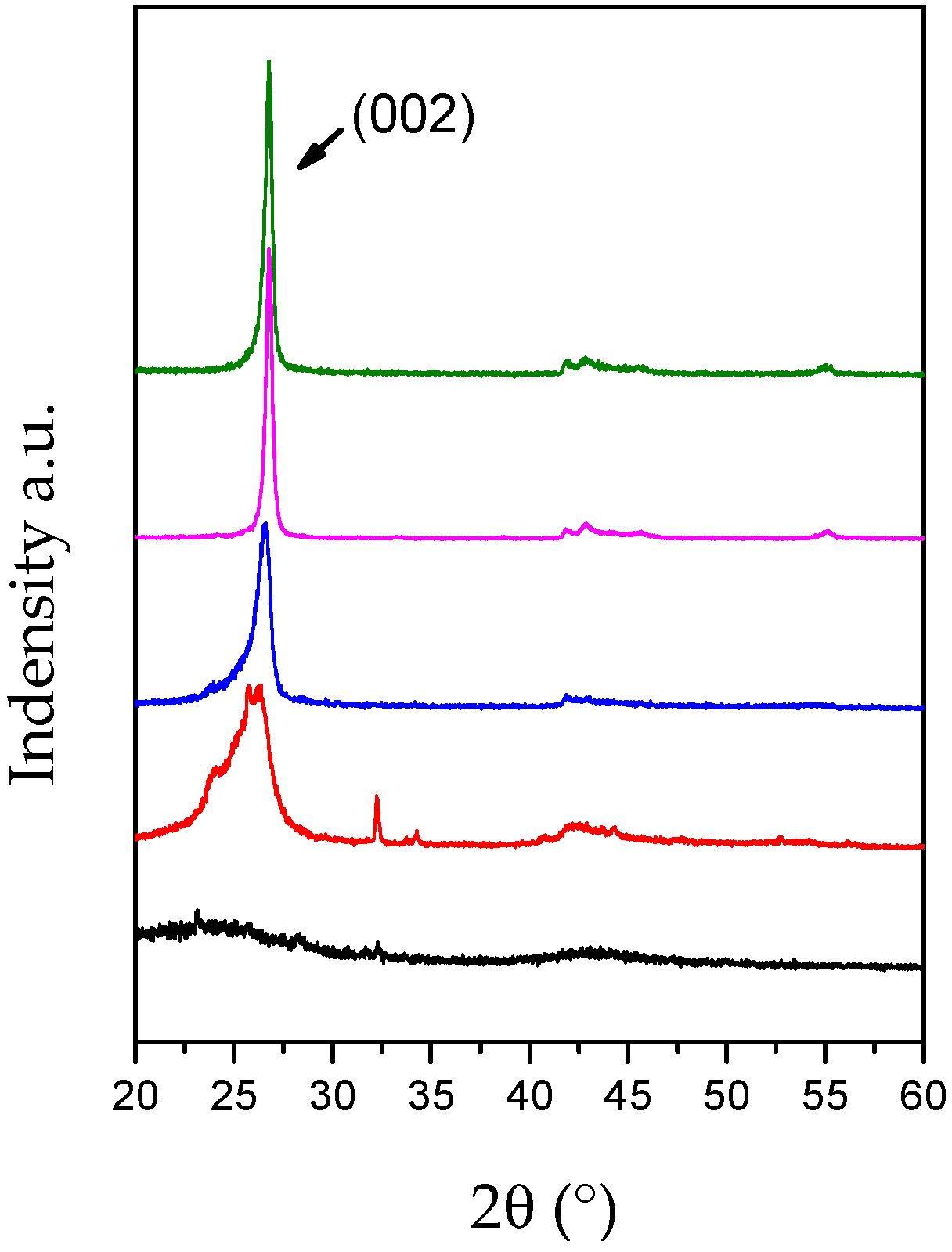
| Sample | θ002 (°) | d002 (Å) 1 | FWHM(002) | Lc (nm) |
|---|---|---|---|---|
| TiBN1200 | 24.5 | 3.60 | 4.83 | 1.7 |
| TiBN1350-9f | 25.8 | 3.44 | 2.9 | 3.0 |
| TiBN1350-6f | 25.3 | 3.52 | 2.8 | 2.9 |
| Sample | d002 (Å) | θ002 (°) | FWHM(002) | θ10 (°) | FWHM(10) | Lc (nm) | La (nm) |
|---|---|---|---|---|---|---|---|
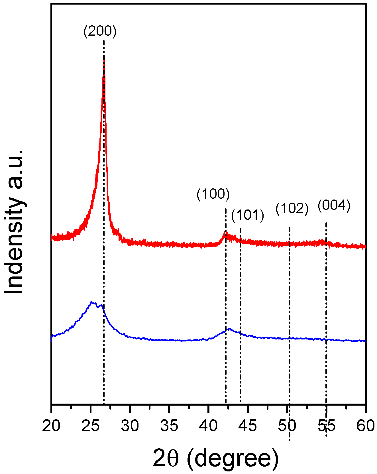
| Commercial h-BN | 3.31 | 26.9 | 0.35 | 41.7 | - | - 1 | - 1 |
| Li3N-PBN | 3.33 | 26.7 | 0.92 | 42.0 | 1.0 | 37.8 | 38.0 |
| PBN | 3.54 | 25.1 | 3.61 | 42.6 | 2.2 | 2.3 | 8.6 |
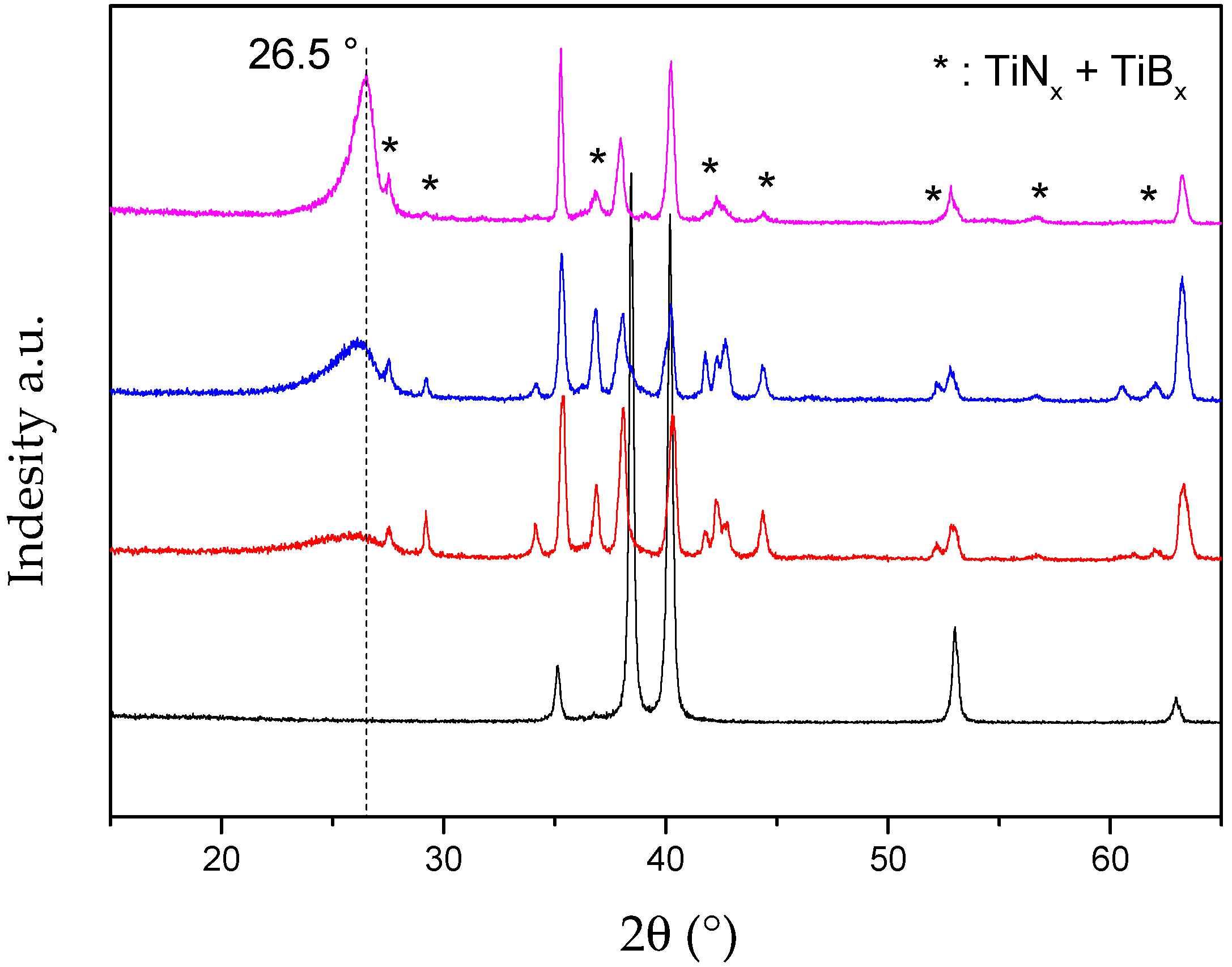
| Sample | d002 (Å) | θ002 (°) | FWHM(002) | Lc (nm) |
|---|---|---|---|---|
| TiBN5 | 3.33 | 26.6 | 0.67 | 26 |
| TiBN3 | 3.41 | 26.1 | 0.92 | 19 |
| TiBN1 | 3.55 | 25.9 | 1.54 | 11 |
| Signal intensity | (200) | (100) | (101) | (102) | (004) | (110) | (112) |
|---|---|---|---|---|---|---|---|
| Theoretical Intensity | 100 | 15 | 6 | 15 | 6 | 5 | 5 |
| Calculated intensity | 100 | 3.7 | 2.5 | 0 | 5 | 2.8 | 2 |
© 2016 by the authors; licensee MDPI, Basel, Switzerland. This article is an open access article distributed under the terms and conditions of the Creative Commons Attribution (CC-BY) license (http://creativecommons.org/licenses/by/4.0/).
Share and Cite
Yuan, S.; Journet, C.; Linas, S.; Garnier, V.; Steyer, P.; Benayoun, S.; Brioude, A.; Toury, B. How to Increase the h-BN Crystallinity of Microfilms and Self-Standing Nanosheets: A Review of the Different Strategies Using the PDCs Route. Crystals 2016, 6, 55. https://doi.org/10.3390/cryst6050055
Yuan S, Journet C, Linas S, Garnier V, Steyer P, Benayoun S, Brioude A, Toury B. How to Increase the h-BN Crystallinity of Microfilms and Self-Standing Nanosheets: A Review of the Different Strategies Using the PDCs Route. Crystals. 2016; 6(5):55. https://doi.org/10.3390/cryst6050055
Chicago/Turabian StyleYuan, Sheng, Catherine Journet, Sébastien Linas, Vincent Garnier, Philippe Steyer, Stéphane Benayoun, Arnaud Brioude, and Bérangère Toury. 2016. "How to Increase the h-BN Crystallinity of Microfilms and Self-Standing Nanosheets: A Review of the Different Strategies Using the PDCs Route" Crystals 6, no. 5: 55. https://doi.org/10.3390/cryst6050055