
Freeform Phononic Waveguides


Department of Physics, Advanced Technology Institute, University of Surrey, Guildford, Surrey GU2 7XH, UK
*
Author to whom correspondence should be addressed.
Crystals 2017, 7(12), 353; https://doi.org/10.3390/cryst7120353
Submission received: 15 October 2017
/
Revised: 13 November 2017
/
Accepted: 24 November 2017
/
Published: 28 November 2017
(This article belongs to the Special Issue Phononics)
Abstract
:We employ a recently introduced class of artificial structurally-disordered phononic structures that exhibit large and robust elastic frequency band gaps for efficient phonon guiding. Phononic crystals are periodic structures that prohibit the propagation of elastic waves through destructive interference and exhibit large band gaps and ballistic propagation of elastic waves in the permitted frequency ranges. In contrast, random-structured materials do not exhibit band gaps and favour localization or diffusive propagation. Here, we use structures with correlated disorder constructed from the so-called stealthy hyperuniform disordered point patterns, which can smoothly vary from completely random to periodic (full order) by adjusting a single parameter. Such amorphous-like structures exhibit large band gaps (comparable to the periodic ones), both ballistic-like and diffusive propagation of elastic waves, and a large number of localized modes near the band edges. The presence of large elastic band gaps allows the creation of waveguides in hyperuniform materials, and we analyse various waveguide architectures displaying nearly 100% transmission in the GHz regime. Such phononic-circuit architectures are expected to have a direct impact on integrated micro-electro-mechanical filters and modulators for wireless communications and acousto-optical sensing applications.
1. Introduction
Phononic crystals are artificial materials with periodically arranged components. They were introduced more than two decades ago as the elastic waves’ analogue of photonic crystals [1]. These materials can exhibit large frequency regions of prohibited propagation of elastic waves—the so-called phononic band gaps (PBGs)—in either two or three dimensions. Phononic band gap materials [2] have a direct impact on a vast number of applications, including audible filters [3], acoustic diodes [4], ultrasound imaging [5], optomechanics [6], heat conduction, and energy harvesting [7,8,9,10], etc. On the other hand, disorder in elastic media [11,12,13,14] is important for a large range of applications including acoustic filters [15], piezoelectric materials [16], biological materials [17], fracture [18], and manipulation of the thermal conductance [7,19], etc. Despite this and in contrast to the vast body of studies dealing with the effects of disorder on photonic structures, the research of disordered phononic systems and the effect of disorder on phononic band gaps has been sparse, with a few notable exceptions [12,20,21,22].
In general, hyperuniform disordered structures [23], which exhibit short- and long-range uniformity, have been investigated in the last decade as an intermediate regime between ordered and totally (uncorrelated) disordered structures [20,21,24] and have received increasing attention in the context of controlling the flow of electromagnetic radiation at the micron scale. The recently introduced hyperuniform disordered phononic structures (HDPS) [21], have the advantage of combining the properties of both periodic and random counterpart extremes. This combination makes them ideal for phonon manipulation since they can exhibit large band gaps, statistical isotropy, localization, and diffusive propagation at the same time. In this work, we theoretically analyse propagation of elastic waves in the GHz frequency region and extensively explore various architecture designs to discuss 2D and 3D waveguided architectures. We demonstrate that waveguides in hyperuniform structures display transmission field profiles with nearly 100% transmission in for a very thin, freeform-shape 3D waveguided architecture.
2. Phononic Band Gaps in Two-Dimensional HDPS
2.1. The Hyperuniform Structure
In this work, we consider a hyperuniform point pattern made [25,26] of 500 points distributed within a square of 22.4-m side length, using periodic boundary conditions for the box (super-cell) as shown in the left-hand panel of Figure 1.
The diffraction pattern, proportional to the intensity of the Fourier (shown in the right-hand panel of Figure 1), exhibits a disk of practically zero interior intensity, with a radius 2.5 m, corresponding to a stealthy parameter of [25]. The average distance among the cylinders is 1 m and the diameter of each cylinder is 0.5 m. For material parameters, we consider that the cylinders are made of lead with density of 11.4 g/cm, shear wave velocity of 860 m/s, and longitudinal wave velocity of 2160 m/s. The surrounding matrix is assumed to consist of epoxy with density of 1.2 g/cm, shear wave of velocity 1160 m/s, and longitudinal wave velocity of 2830 m/s. These parameters have been used in the study of disorder in phononic structures in the past [14] and provide optimized band gaps for the corresponding periodic structures.
2.2. Band Structure for Out-of-Plane Elastic Wave Modes
We start our discussion with 2D structures, i.e., assuming infinite (homogeneous) extent along the third (z) dimension. In this case, elastic waves polarized within the plane propagate independently of elastic waves polarized normal to this plane. All the results are obtained from theoretical simulations with the help of well-established finite element commercial software (COMSOL Multiphysics®). The scattering cross for a (shear) out-of-plane polarized incident plane wave is shown in Figure 2a. The isolated cylinder is excited at 0.28 GHz, with z component of the elastic field and the mode profile shown in the Figure 2a (inset). When considering a photonic crystal made out of identical cylinders, the mode described above hybridizes and evolves in the mode located at the lower edge of the phononic band gap. This mode contributes to the opening of the band gap, which in the case of a square periodic structure (PC) of lattice constant a = 1 m has a relative size of 64%, extending from 0.36 GHz to 0.70 GHz, as shown in Figure 2b. The band structure of the HDPS made of of identical cylinders (Figure 1a) is shown in Figure 2c. We note that, due to the 500-time folding of the BS (compared to the periodic case), the bands appear almost flat. However, the effective velocity in both the PC and the HDPS remains the same in the long wavelength limit. Figure 2d shows that the transmission from a finite (along the x axis) slab of the structure becomes very small in the region of the band gap, as expected. Compared to previous approaches in correlated disordered phononic structures [13,14], we find band gaps of similar size. However, we emphasize that our structures originate from completely disordered structures, without any signature of an underlying periodicity, and are hence much more flexible. We will exploit this for the design freeform waveguides. Moreover, we also note that as the parameter decreases, disorder and non-uniformity of the structure increase and, as a result, the size band gap also decreases. Therefore, in the current study we keep the value fixed to 0.5 to achieve the largest band gap and hence, the spectral range over which freeform waveguiding can be implemented.
2.3. Band Structure for in-Plane Elastic Wave Modes
The scattering cross for a shear in-plane polarized incident plane wave is shown in Figure 3a. We consider excitation of a mode of the cylinder at 0.64 GHz, with the magnitude of the elastic field shown in the inset of Figure 3a. In the case of the photonic crystal structure, this evolves again in the lower edge mode of the phononic band gap. In the case of a square PC of lattice constant a = 1 m, the phononic band gap has a relative size of 32%, extending from 0.67 GHz to 0.93 GHz, as shown in Figure 3b. The band structure of the HDPS Figure 1a is shown in Figure 3c. We note again that, due to the folding of the band structure, the bands appear almost flat. The effective velocity in both the PC and the HDPS remains the same in the long wavelength limit. However, the band gap decreases a little bit (relative size 26%) extending from 0.67 GHz to 0.87 GHz. We also note that the coincidence of the lower band edge in the two cases is related to the existence of the single-cylinder mode described above, which develops into the lower band-edge mode in both the periodic and disordered structure cases. Figure 3d shows that the transmission from a finite (along the x axis) slab of the structure becomes very small, for both in-plane shear (polarized along the y axis) and longitudinal (polarized along the x axis) incident waves in the region of the band gap.
3. Freeform Waveguides
3.1. 2D Modes in Nearly-Hyperuniform Structures
The existence of large band gaps in the HDPS can be exploited to construct efficient waveguide structures. We employ here the bottom-up approach discussed previously [21,27,28,29,30], which leads to a nearly-hyperuniform distribution of points. Specifically, we consider an arbitrarily-shaped waveguide path formed by equidistant scattering centres and surrounded by a bulk hyperuniform-like material. In contrast to previous works, we assume here only a single line of equidistant cylinders homogeneously aligned parallel to the waveguide path. The rest of the structure is defined within a square region of side 40 m. The position of the points is found by minimizing a repelling potential of the form , r being the distance among the points, under periodic boundary conditions. In total, we consider 1600 points within our domain, decorated with identical cylinders. We consider three different arbitrary waveguide paths, as shown in Figure 4. All these paths have a continuously changing slope throughout the entire shape and therefore cannot be implemented on a photonic crystal platform. While for some of the paths one can identify alternatives possible to implement in either periodic phononic crystals or curvilinear defined periodic structures, the hyperuniform-like platform described here allows for ultimate flexibility both in terms of the arbitrariness of the waveguide path and the ability to accommodate various freeform designs on a single platform. The unique feature is directly related to the nearly-deal statistical isotropy and homogeneity of the hyperuniform surround.
3.2. Out-of-Plane 2D Waveguide Modes
Transmission for the out-of-plane modes through these arbitrary-shaped waveguide is shown in Figure 5a, together with transmission of a straight waveguide. Our results demonstrate that in the region of the band gap, the freeform HDPS waveguides provide efficient guiding as compared to the straight waveguide. In the case of the 90°-bend waveguide, the efficiency drops after 0.6 GHz, while for the hyperbolic tangent shaped waveguide, the efficiency is remains high up to 0.6 GHz. We also note that in the high transmission regions, the elastic field is nearly perfectly confined around the waveguide path (Figure 5b–e).
3.3. In-Plane 2D Waveguide Modes
Transmission for the in-plane modes through these arbitrary shaped waveguide is shown in Figure 6a, together with transmission of a straight waveguide. In the region around 0.7 GHz and 0.8 GHz, the efficiency of the freeform waveguides reaches 100%. We also note that at the high transmission regions, the fields are again very well localized around the waveguide path, as shown in Figure 6b–e. The sharp drops of the transmission for the arbitrary shaped waveguides are due to excitation of localized modes at the sharper corners of the bends, which block transmission at certain frequencies. These regions of low-transmission could, in principle, be eliminated through further optimisation of the waveguide surround. Elsewhere, transmission is comparable to that of a periodic straight waveguide. Moreover, lower-efficiency waveguiding occurs even beyond the spectral region of the phononic band gap.
3.4. Waveguide Modes in 3D Slabs
Motivated by the recent progrss in the fabrication of finite-height hypersonic band gap structures [31,32,33], we now consider a realistic 3D slab architecture. For simplicity, we assume that our structure is suspended in air. In this case the modes of the out-of-plane and in-plane polarization are no longer separable. Hence, we do not expect an absolute band gap, since there is no spectral overlap between the out-of-plane and in-plane band gaps found in the 2D structures. However, these structures exhibit spectral regions of very low transmission [21], which we plan to exploit to create practical 3D slab waveguides with a height equal to the average separation distance of the cylinders, i.e., 1 m. We note that for much larger heights the finite size effects should be minimal and therefore one should retrieve the same results as in the 2D case.
In Figure 7, we identify a nearly-optimal confined waveguided mode at a frequency of 0.52 GHz, displaying overall transmission above 95%. We note that due to the suspended-membrane architecture, the main losses are related to in-slab propagation outside the waveguide channel. While the vertical losses do not play a major role, in order to improve the guiding performance and extend the spectral range over which the guiding occurs, further optimization of the structure may be necessary. The main main target of such an optimization procedure would be to identify configurations that allow for the formation of a complete 2D band, which can be employed in 3D slab architectures. However, such an optimization and the the study broadband response of the waveguide architecture is a computer resource-intensive problem and is beyond the scope of our study.
4. Conclusions
We have analysed structurally-disordered hyperuniform phononic crystals (HDPS). These structures originate from random point patterns by optimizing their Fourier spectrum to achieve an isotropic structure factor that vanishes for all vectors within a specific radius. The resulting hyperuniform structures display amorphous-like short-range ordering and well-defined long-range uniformity (Figure 1), with an average separation distance of 1 m among cylinders. In such structures both ballistic-like propagation (at lower wavelengths) and diffusive transport (at higher frequencies) together with large and robust phononic band gaps coexist. By using finite-element methods and supercell techniques, we have calculated the band structure of HDPS in the sub-GHz regime. Large PBGs, comparable to their periodic counterparts, have been identified, accompanied by huge transmission drops in the relevant frequency regions for all possible polarizations. We note that our results should be qualitatively similar for a wide range of material parameters, provided that a strong enough contrast between the cylinders and the matrix is maintained [31,32,33].
We have shown that the presence of the phononic band gaps in hyperuniform disordered structures makes them ideal candidates for the implementation of highly efficient, freeform waveguides. There is a high efficiency of such structures as arbitrary-shaped waveguides in 2D (very large height). The designed waveguides perform very well for both in-plane and out-of-plane polarization guiding and even for 3D-slab waveguide architectures. Our study predicts transmission efficiency up to 100% within the frequency regions of the band gaps of the relevant HDPS for the freeform waveguides. Our findings can provide a significant advance in the design of phononic integrated circuits providing a versatile platform on which various circuit elements can be connected with highly-efficient waveguides following arbitrary-shaped pathways. Although we have focused on microscale applications, we expect that the understanding and control of such coupling between random and short-range ordered structures is important for other length-scale regimes, e.g., macroscale, for exploring seismic wave propagation in correlated disorder materials, fracture in complex structures, and the nanoscale in applications related to thermal transport.
Supplementary Materials
The data underlying the findings of this study are available without restriction. Details of the data and how to request access are available from the University of Surrey publications repository: http://doi.org/10.15126/surreydata.00845033.
Acknowledgments
This work was partially supported by the University of Surrey’s IAA award to MF, EPSRC (United Kingdom) Strategic Equipment Grant No. EP/L02263X/1 (EP/M008576/1) and EPSRC (United Kingdom) Grant EP/M027791/1.
Author Contributions
Marian Florescu initiated the programme, oversaw and directed the project, designed the waveguide architectures and wrote the paper. Georgios Gkantzounis designed the waveguide architectures, performed simulations and wrote the paper.
Conflicts of Interest
The authors declare no conflict of interest.
References
- Kushwaha, M.S.; Halevi, P. Band-gap engineering in periodic elastic composites. Appl. Phys. Lett. 1994, 64, 1085. [Google Scholar]
- Deymier, P.A. Acoustic Metamaterials and Phononic Crystals; Springer Science & Business Media: New York, NY, USA, 2013; Volume 173. [Google Scholar]
- Vasseur, J.O.; Deymier, P.A.; Khelif, A.; Lambin, P.; Djafari-Rouhani, B.; Akjouj, A.; Dobrzynski, L.; Fettouhi, N.; Zemmouri, J. Phononic crystal with low filling fraction and absolute acoustic band gap in the audible frequency range: A theoretical and experimental study. Phys. Rev. E 2002, 65, 056608. [Google Scholar]
- Li, X.F.; Ni, X.; Feng, L.; Lu, M.H.; He, C.; Chen, Y.F. Tunable unidirectional sound propagation through a sonic-crystal-based acoustic diode. Phys. Rev. Lett. 2011, 106, 084301. [Google Scholar]
- Sukhovich, A.; Jing, L.; Page, J.H. Negative refraction and focusing of ultrasound in two-dimensional phononic crystals. Phys. Rev. B 2008, 77, 014301. [Google Scholar]
- Aspelmeyer, M.; Kippenberg, T.J.; Marquardt, F. Cavity optomechanics. Rev. Mod. Phys. 2014, 86, 1391–1452. [Google Scholar]
- Maldovan, M. Sound and heat revolutions in phononics. Nature 2013, 503, 209217. [Google Scholar]
- Davis, B.L.; Hussein, M.I. Nanophononic metamaterial: Thermal conductivity reduction by local resonance. Phys. Rev. Lett. 2014, 112, 055505. [Google Scholar]
- Lv, H.; Tian, X.; Wang, M.Y.; Li, D. Vibration energy harvesting using a phononic crystal with point defect states. Appl. Phys. Lett. 2013, 102, 034103. [Google Scholar]
- Schuler, C.J.; Wolff, C.; Busch, K.; Florescu, M. Thermal emission from finite photonic crystals. Appl. Phys. Lett. 2009, 95, 241103. [Google Scholar] [Green Version]
- Yuan, Z.D.; Chen, J.C. Elastic wave propagation in two-dimensional ordered and weakly disordered phononic crystals. Chin. Phys. Lett. 2005, 22, 889–891. [Google Scholar]
- Wagner, M.R.; Graczykowski, B.; Reparaz, J.S.; Sachat, A.E.; Sledzinska, M.; Alzina, F.; Torres, C.M.S. Two-Dimensional phononic crystals: Disorder matters. Nano Lett. 2016, 16, 5661–5668. [Google Scholar]
- Still, T.; Cheng, W.; Retsch, M.; Sainidou, R.; Wang, J.; Jonas, U.; Stefanou, N.; Fytas, G. Simultaneous occurrence of structure-directed and particle-resonance-induced phononic gaps in colloidal films. Phys. Rev. Lett. 2008, 100, 194301. [Google Scholar]
- Chen, A.L.; Wang, Y.S. Study on band gaps of elastic waves propagating in one-dimensional disordered phononic crystals. Physica B 2007, 392, 369–378. [Google Scholar]
- Tourin, A.; Van Der Biest, F.; Fink, M. Time reversal of ultrasound through a phononic crystal. Phys. Rev. Lett. 2006, 96, 104301. [Google Scholar]
- Wang, Y.Z.; Li, F.M.; Huang, W.H.; Wang, Y.S. The propagation and localization of Rayleigh waves in disordered piezoelectric phononic crystals. J. Mech. Phys. Solids 2008, 56, 1578–1590. [Google Scholar]
- Davies, B.; King, A.; Newman, P.; Minett, A.; Dunstan, C.R.; Zreiqat, H. Hypothesis: Bones toughness arises from the suppression of elastic waves. Sci. Rep. 2014, 4, 7538. [Google Scholar]
- Shekhawat, A.; Zapperi, S.; Sethna, J.P. From damage percolation to crack nucleation through finite size criticality. Phys. Rev. Lett. 2013, 110, 185505. [Google Scholar]
- Zen, N.; Puurtinen, T.A.; Isotalo, T.J.; Chaudhuri, S.; Maasilta, I.J. Engineering thermal conductance using a two-dimensional phononic crystal. Nat. Commun. 2014, 5, 3435. [Google Scholar]
- Limonov, M.F.; De La Rue, R.M. Optical Properties of Photonic Structures: Interplay of Order and Disorder; CRC Press, Taylor & Francis Group: Boca Raton, FL, USA, 2012. [Google Scholar]
- Gkantzounis, G.; Amoah, T.; Florescu, M. Hyperuniform disordered phononic structures. Phys. Rev. B 2017, 95, 094120. [Google Scholar]
- Chen, A.L.; Wang, Y.S.; Li, J.B.; Zhang, C. Localisation of elastic waves in two-dimensional randomly disordered solid phononic crystals. Waves Random Complex 2010, 20, 104–121. [Google Scholar]
- Torquato, S.; Stillinger, F.H. Local density fluctuations, hyperuniformity, and order metrics. Phys. Rev. E 2003, 68, 041113. [Google Scholar]
- Florescu, M.; Torquato, S.; Steinhardt, P.J. Designer disordered materials with large, complete photonic band gaps. Proc. Natl. Acad. Sci. USA 2009, 106, 20658. [Google Scholar]
- Uche, O.U.; Torquato, S.; Stillinger, F.H. Collective coordinates control of density distributions. Phys. Rev. E 2006, 74, 031104. [Google Scholar]
- Batten, R.D.; Stillinger, F.H.; Torquato, S. Classical disordered ground states: Super-Ideal gases, and stealth and equi-luminous materials. J. Appl. Phys. 2008, 104, 033504. [Google Scholar]
- Florescu, M.; Torquato, S.; Steinhardt, P.J. Effects of random link removal on the photonic band gaps of honeycomb networks. Appl. Phys. Lett. 2010, 97, 10–13. [Google Scholar]
- Amoah, T.; Florescu, M. High-Q optical cavities in hyperuniform disordered materials. Phys. Rev. B 2015, 91, 020201(R). [Google Scholar]
- Tsitrin, S.; Williamson, E.P.; Amoah, T.; Nahal, G.; Chan, H.L.; Florescu, M.; Man, W. Unfolding the band structure of non-crystalline photonic band gap materials. Sci. Rep. 2015, 5, 13301. [Google Scholar] [Green Version]
- Sellers, S.R.; Man, W.; Sahba, S.; Florescu, M. Local self-uniformity in photonic networks. Nat. Commun. 2017, 8, 14439. [Google Scholar]
- Sato, A.; Pennec, Y.; Yanagishita, T.; Masuda, H.; Knoll, W.; Djafari-Rouhani, B.; Fytas, G. Cavity-type hypersonic phononic crystals. New J. Phys. 2012, 14, 113032. [Google Scholar]
- Yudistira, D.; Boes, A.; Graczykowski, B.; Alzina, F.; Yeo, L.Y.; Sotomayor Torres, C.M.; Mitchell, A. Nanoscale pillar hypersonic surface phononic crystals. Phys. Rev. B 2016, 94, 094304. [Google Scholar]
- Gorishnyy, T.; Ullal, C.K.; Maldovan, M.; Fytas, G.; Thomas, E.L. Hypersonic phononic crystals. Phys. Rev. Lett. 2005, 94, 115501. [Google Scholar]
Figure 1.
(a) The 2D structure considered in this work and (b) its corresponding diffraction pattern.
Figure 1.
(a) The 2D structure considered in this work and (b) its corresponding diffraction pattern.
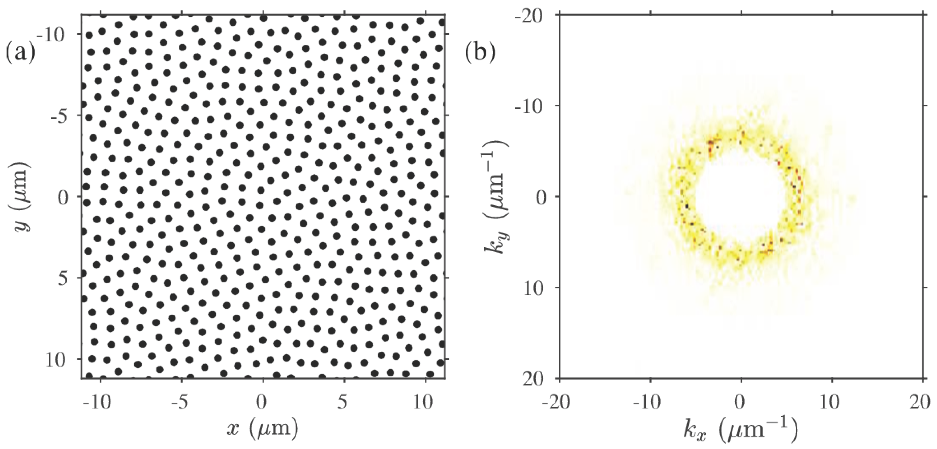
Figure 2.
Out-of-plane modes. (a) Scattering cross section of a single Pb (infinite) cylinder in epoxy. The z component of the elastic field for excitation from the left with a z-polarized plane wave at 0.28 GHz is shown in the inset (black circle denotes the position of the cylinder). (b) The 2D band structure of the periodic crystal of Pb in epoxy. The horizontal broken lines denote the band gap edges of the hyperuniform disordered phononic structures (HDPS). (c) The 2D band structure of the HDPS. (d) Transmission of the HDPS for a z- polarized incident plane wave.
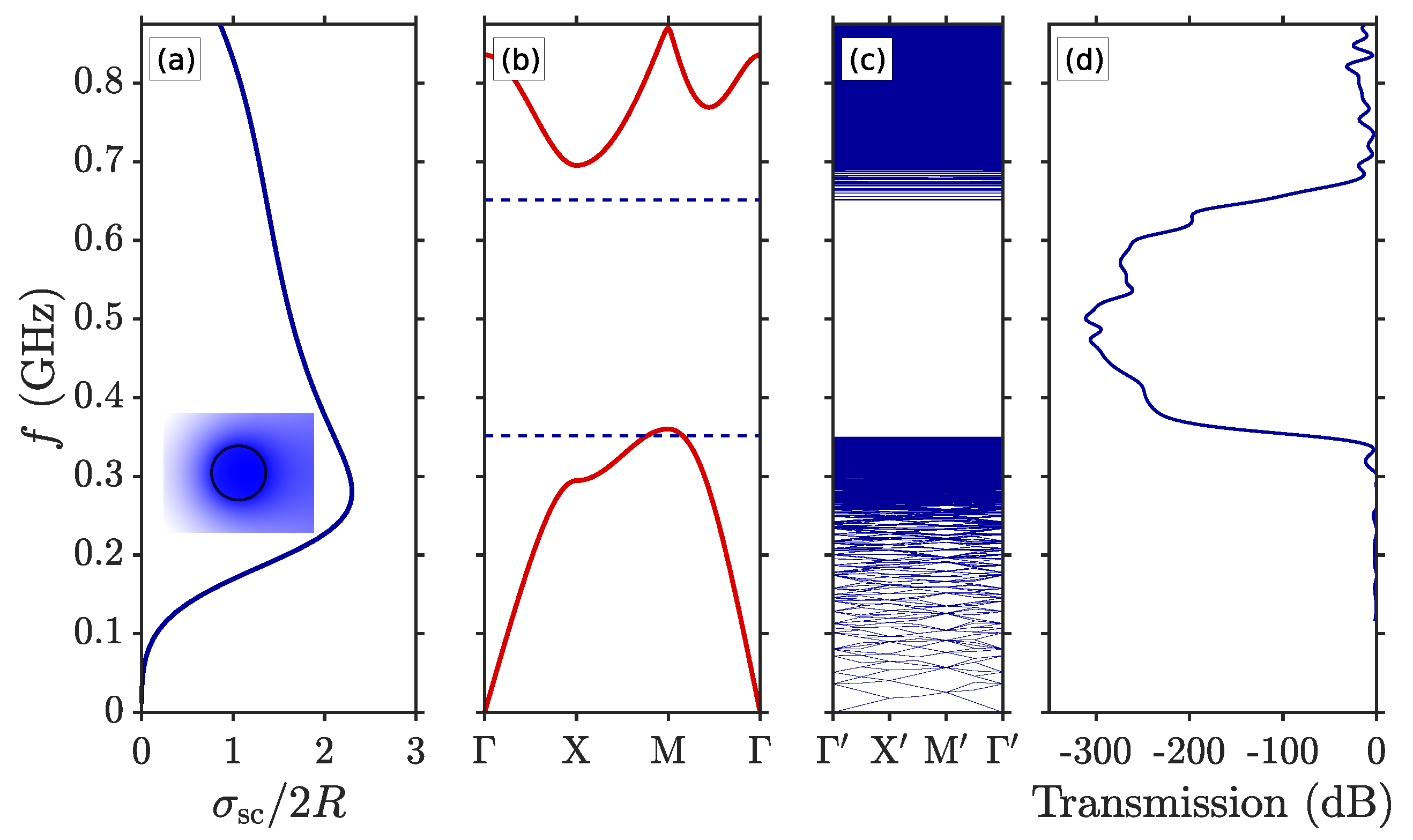
Figure 3.
In-plane modes. (a) Scattering cross section of a single Pb (infinite) cylinder in epoxy. The magnitude of the elastic field for excitation from the left with a shear plane wave at 0.64 GHz is shown in the inset (black circle denotes the position of the cylinder). (b) The 2D band structure of the periodic crystal of Pb in epoxy. The horizontal broken lines denote the band gap edges of the HDPS. (c) The 2D band structure of the HDPS. (d) Transmission of the HDPS for the longitudinal (solid line) and transverse (dashed line) incident plane wave.
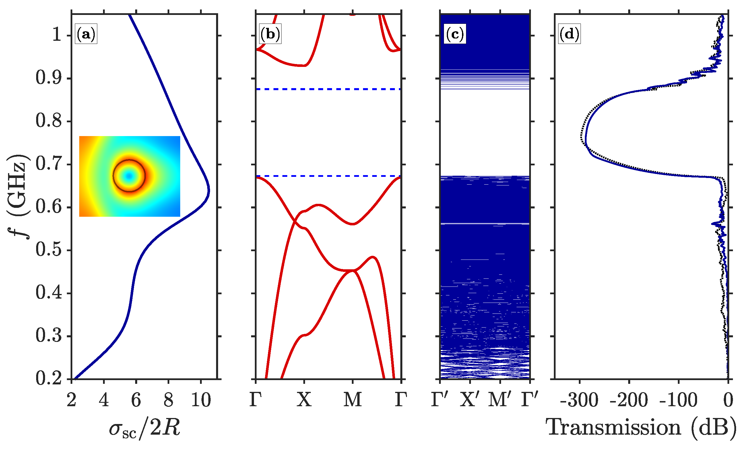
Figure 4.
(a) A hyperbolic tangent-shaped waveguide; (b) a cosine-shaped waveguide; and (c) a 90°-bend waveguide.
Figure 4.
(a) A hyperbolic tangent-shaped waveguide; (b) a cosine-shaped waveguide; and (c) a 90°-bend waveguide.
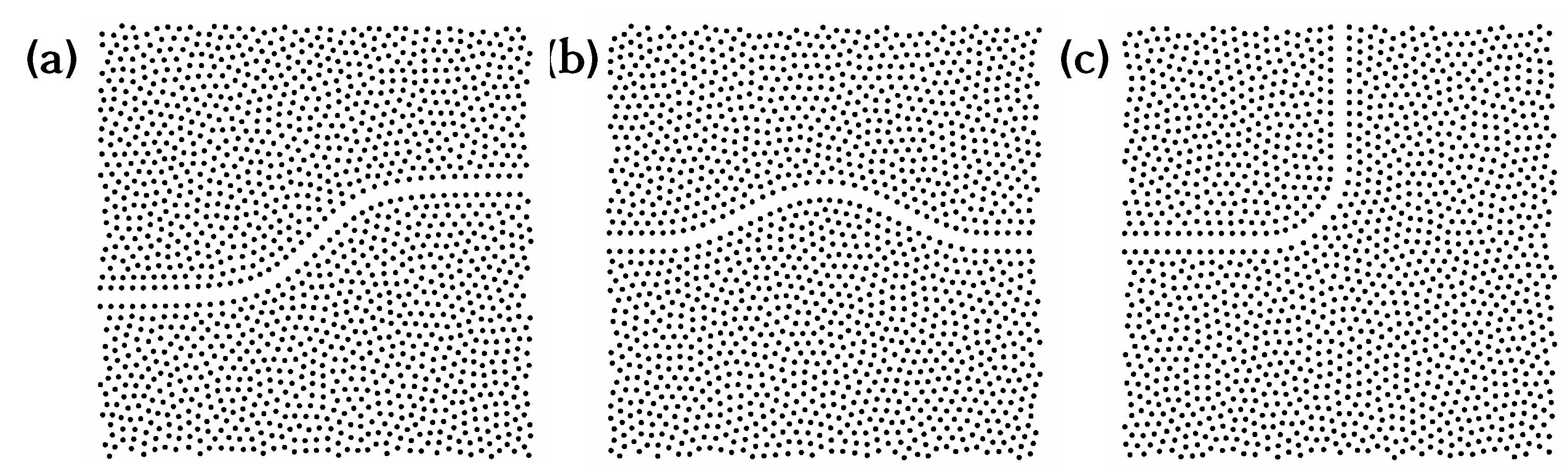
Figure 5.
(a) Transmission of the out-of-plane 2D modes for the waveguides in Figure 4a,c is shown by the blue, red, and green lines, respectively. With the black lines the corresponding transmitted power of a straight waveguide is shown with the black line for comparision. A snapshot of the elastic field vertical component at a propagating frequency of 0.46 GHz is shown in (b–d) for the straight waveguide, and the waveguides in Figure 4a,c, respectively.
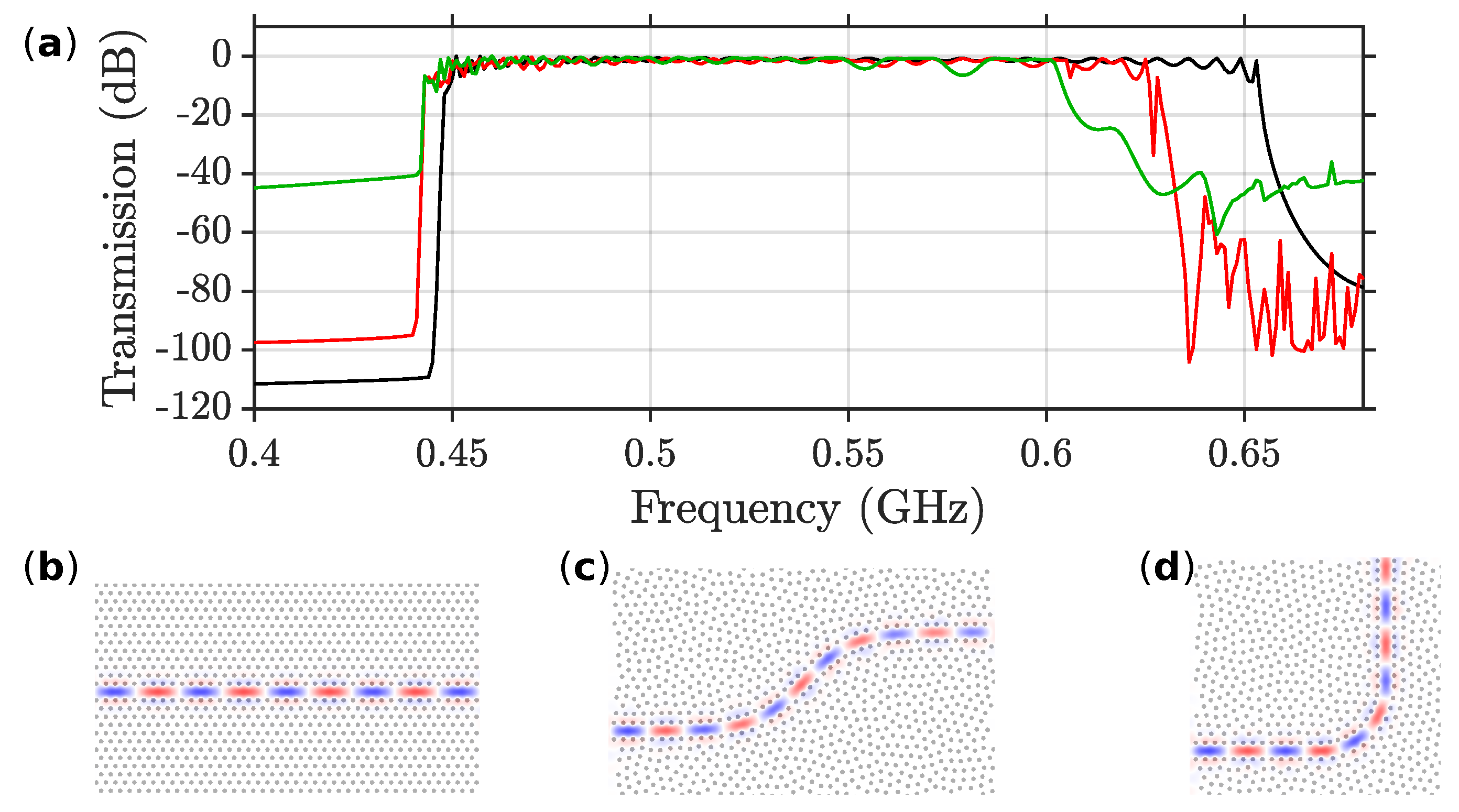
Figure 6.
(a) Transmitted power for the waveguides in Figure 4a–c as shown by the blue, red, and green lines, respectively. With the black lines the corresponding transmitted power of a straight waveguide is shown with the black line for comparision. A snapshot of the elastic field magnitude at a propagating frequency of 0.71 GHz is shown in (b–e) for the straight waveguide, and the waveguides in Figure 4a–c, respectively.
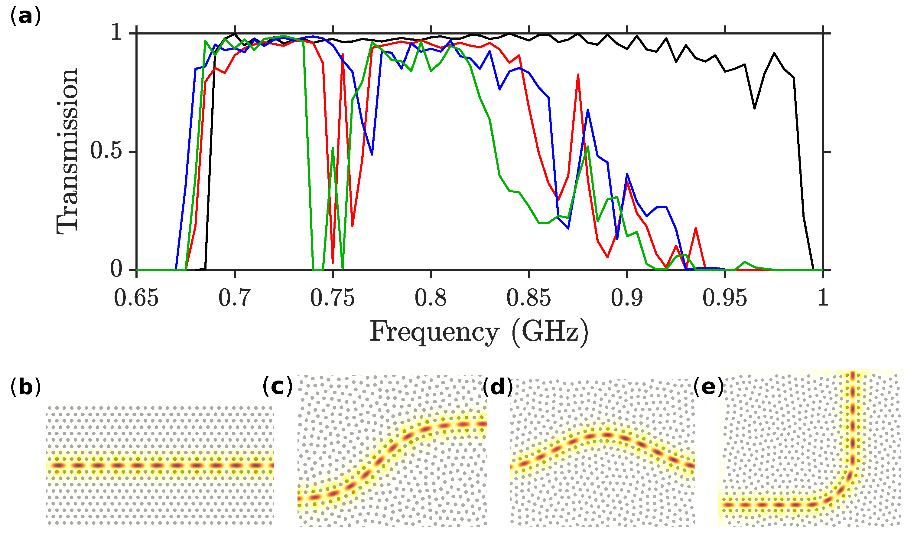
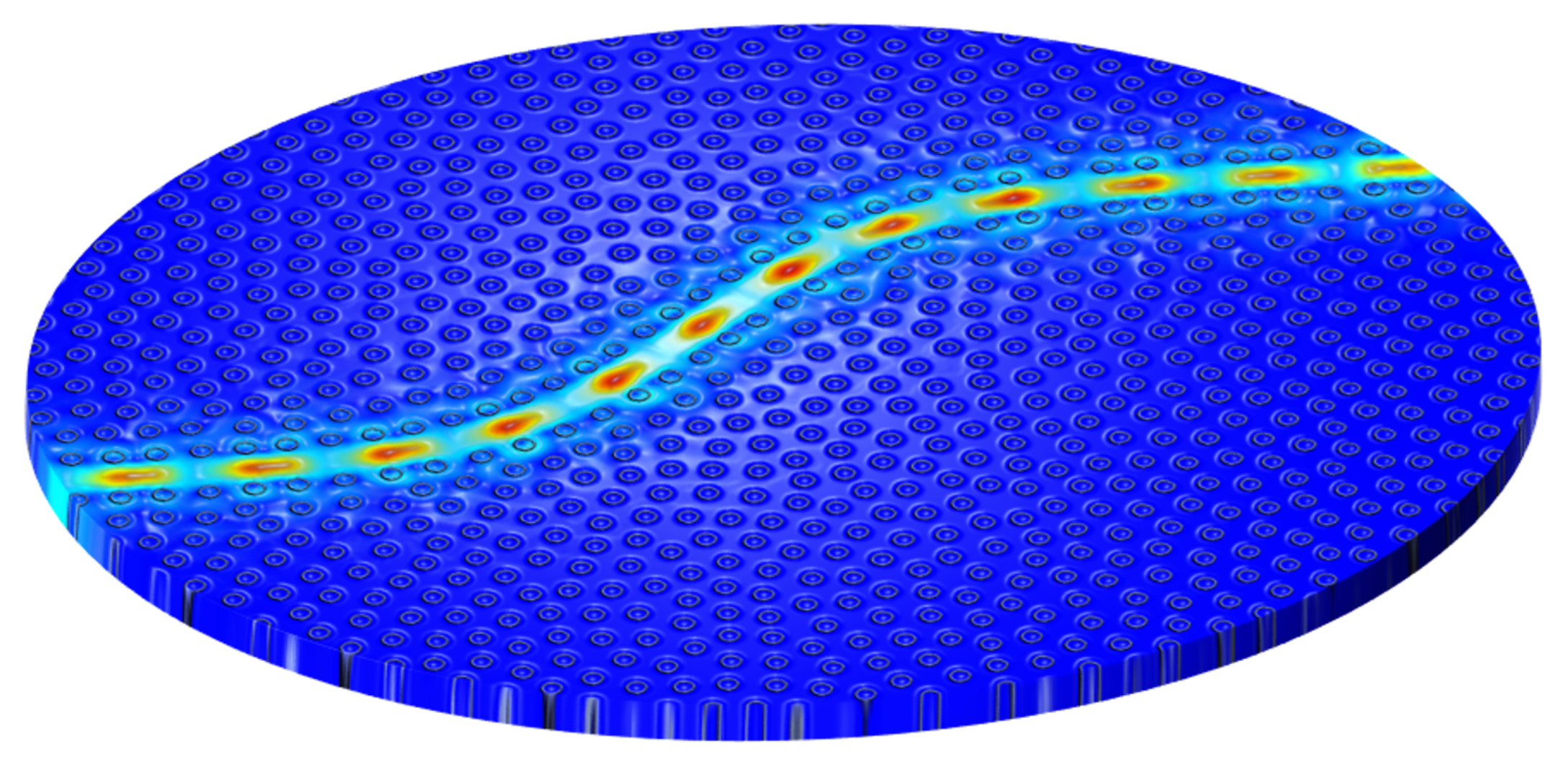
Figure 7.
Snapshot of the elastic field profile at an incident wave frequency of 0.52 GHz for the waveguide shown in Figure 4a, with a finite height of 1 m. The color scale represents the magnitude of the elastic field while the local disturbance is proportional (with orders of magnitude larger, for visualization) to the actual disturbance due to the elastic field traveling through the waveguide.

© 2017 by the authors. Licensee MDPI, Basel, Switzerland. This article is an open access article distributed under the terms and conditions of the Creative Commons Attribution (CC BY) license (http://creativecommons.org/licenses/by/4.0/).
Share and Cite
MDPI and ACS Style
Gkantzounis, G.; Florescu, M. Freeform Phononic Waveguides. Crystals 2017, 7, 353. https://doi.org/10.3390/cryst7120353
AMA Style
Gkantzounis G, Florescu M. Freeform Phononic Waveguides. Crystals. 2017; 7(12):353. https://doi.org/10.3390/cryst7120353
Chicago/Turabian StyleGkantzounis, Georgios, and Marian Florescu. 2017. "Freeform Phononic Waveguides" Crystals 7, no. 12: 353. https://doi.org/10.3390/cryst7120353
Note that from the first issue of 2016, this journal uses article numbers instead of page numbers. See further details here.