Article

Graphene-Hexagonal Boron Nitride Heterostructure as a Tunable Phonon–Plasmon Coupling System

Key Laboratory for Wide Band Gap Semiconductor Materials and Devices of Education, School of Microelectronics, Xidian University, Xi’an 710071, China
*
Authors to whom correspondence should be addressed.
Crystals 2017, 7(2), 49; https://doi.org/10.3390/cryst7020049
Submission received: 31 December 2016 / Revised: 30 January 2017 / Accepted: 4 February 2017 / Published: 10 February 2017

Abstract

:
The layered van der Waals (vdW) heterostructure, assembled from monolayer graphene, hexagonal boron nitride (h-BN) and other atomic crystals in various combinations, is emerging as a new paradigm with which to attain desired electronic and optical properties. In this paper, we study theoretically the mid-infrared optical properties of the vdW heterostructure based on the graphene–h-BN system. The light–matter interaction of this heterostructure system is described by the hyperbolic phonon–plasmon polaritons which originate from the coupling modes of surface plasmon polaritons (SPPs) in graphene with hyperbolic phonon polaritons (HPPs) in h-BN. By numerical simulation, we find that the coupling modes are governed by the Fermi level of monolayer graphene, the thickness of the h-BN slab and the mode excitation sequence of SPPs and HPPs. Moreover, the response of the coupling modes of the graphene–h-BN heterostructure on a noble metal layer is also proposed in this paper.

1. Introduction

In recent years, two-dimensional (2D) materials and layered materials including graphene, hexagonal boron nitride (h-BN), and transition metal dichalcogenides (TMDs) have attracted major attention for applications in optoelectronics and technology such as vibrational spectroscopy and stimulated Raman scattering [1,2,3,4,5,6]. Polaritons, hybrid modes of photons and charge dipole carrying excitations in crystals, are also of interest in the heterostructures which are assembled from 2D materials. Polaritons are generally divided into two types: surface plasmon polaritons (SPPs) and phonon polaritons. Such modes have been shown in related applications such as subwavelength imaging [7], quantum information [8,9], and sensing engineering [10]. In the graphene–h-BN vdW heterostructures [11] system we proposed, SPPs and hyperbolic phonon polaritons (HPPs) are established in monolayer graphene and h-BN, respectively. Generally, graphene SPPs are of great interest for extremely small volumes, broad frequency range (in the mid-infrared and terahertz range), ultrahigh speed and very low energy consumption. Remarkably, the strong light–matter interaction in graphene can be controlled effectively by tuning the Fermi energy [12,13], which denotes that graphene SPP can be effectively regulated [14,15,16,17]. However, graphene SPPs damp out quickly due to scattering loss from substrates and impurities. Apart from graphene, h-BN is a van der Walls crystal [18] as well as a wide bandgap (~6 eV) electrical insulator. Furthermore, h-BN also shows natural hyperbolicity [19,20,21,22,23], which means that the relative dielectric constants in-plane and out-of-plane have opposite signs. This property leads to a hyperbolic or indefinite dispersion for electromagnetic waves propagating inside such a material and results in the excitation of surface phonon-polariton mode. In our system, SPPs modes of coherent oscillations of the electron density in graphene and HPPs modes of the atomic vibrations in h-BN produce hybrid plasmon–phonon modes [24,25,26]. These hybrid modes, regarded as an advanced version of 2D metamaterials, can absorb the virtues of both the hyperbolic dielectric h-BN and graphene by offering more freedom to manipulate infrared waves and thus create new functional optical devices. Due to exceptionally narrow resonance linewidths, up to 300 times narrower than the free-space wavelength, hybridized phonon–plasmon polaritons (HPPP) modes have been demonstrated sub-diffraction polariton propagation and sub-wavelength imaging with nanoscale resolution [19,23].
In this paper, we systematically investigated the graphene–h-BN heterostructure system, which shows strong plasmon–phonon coupling resonance in the mid-infrared regime. Moreover, we give more comprehensive discussions on the field patterns and their propagation features associated with the hybrid coupling with graphene, especially when the properties of graphene are varied. The propagation characteristics can be tuned by controlling the Fermi level of graphene. Compared with the model mentioned in the previous paper [23], the effect of the sequence of excitation on the HPPP modes has been investigated in our model. Furthermore, we introduce the metal SPP in our model to further study the coupling modes’ properties. These aspects affect the coupling modes in such a way that they change the optical properties of the stack graphene–h-BN system.

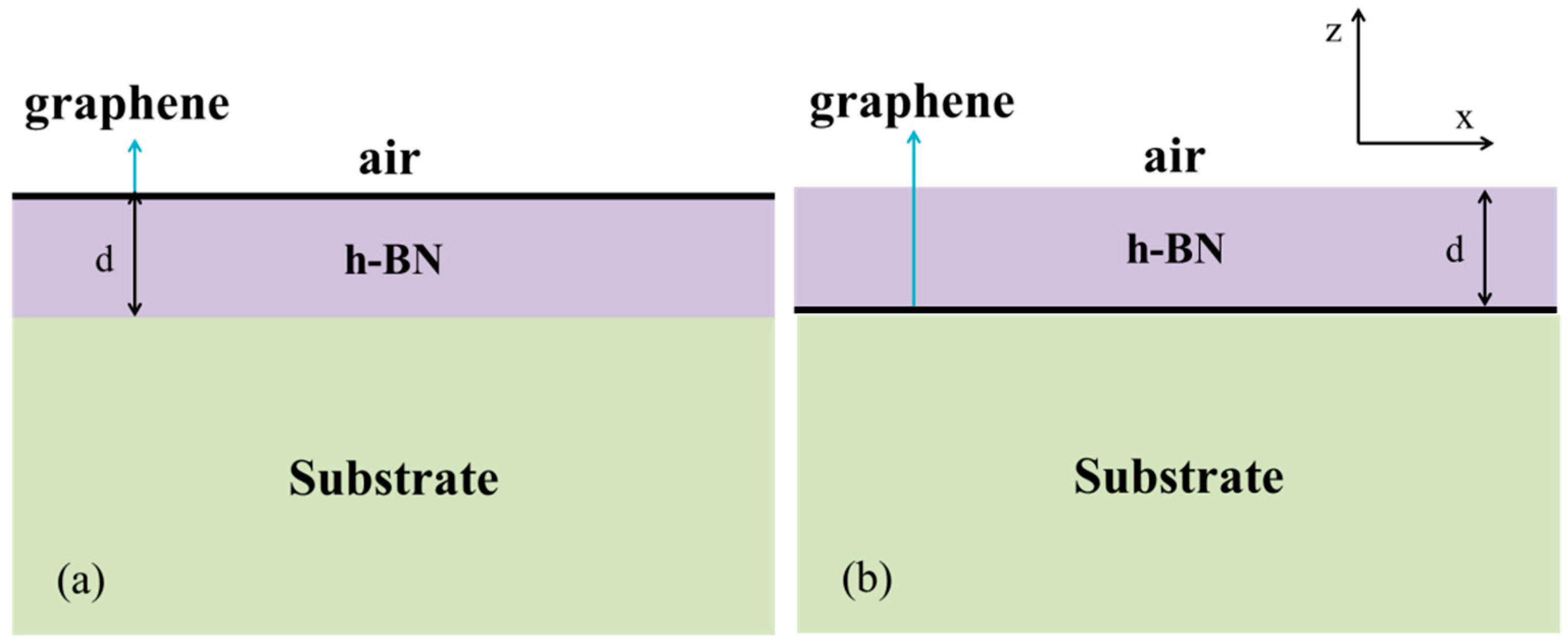
2. Materials and Analysis

In this part, the light–matter properties of different materials in our coupling system are discussed.

2.1 Optical Response Functions of h-BN and Graphene

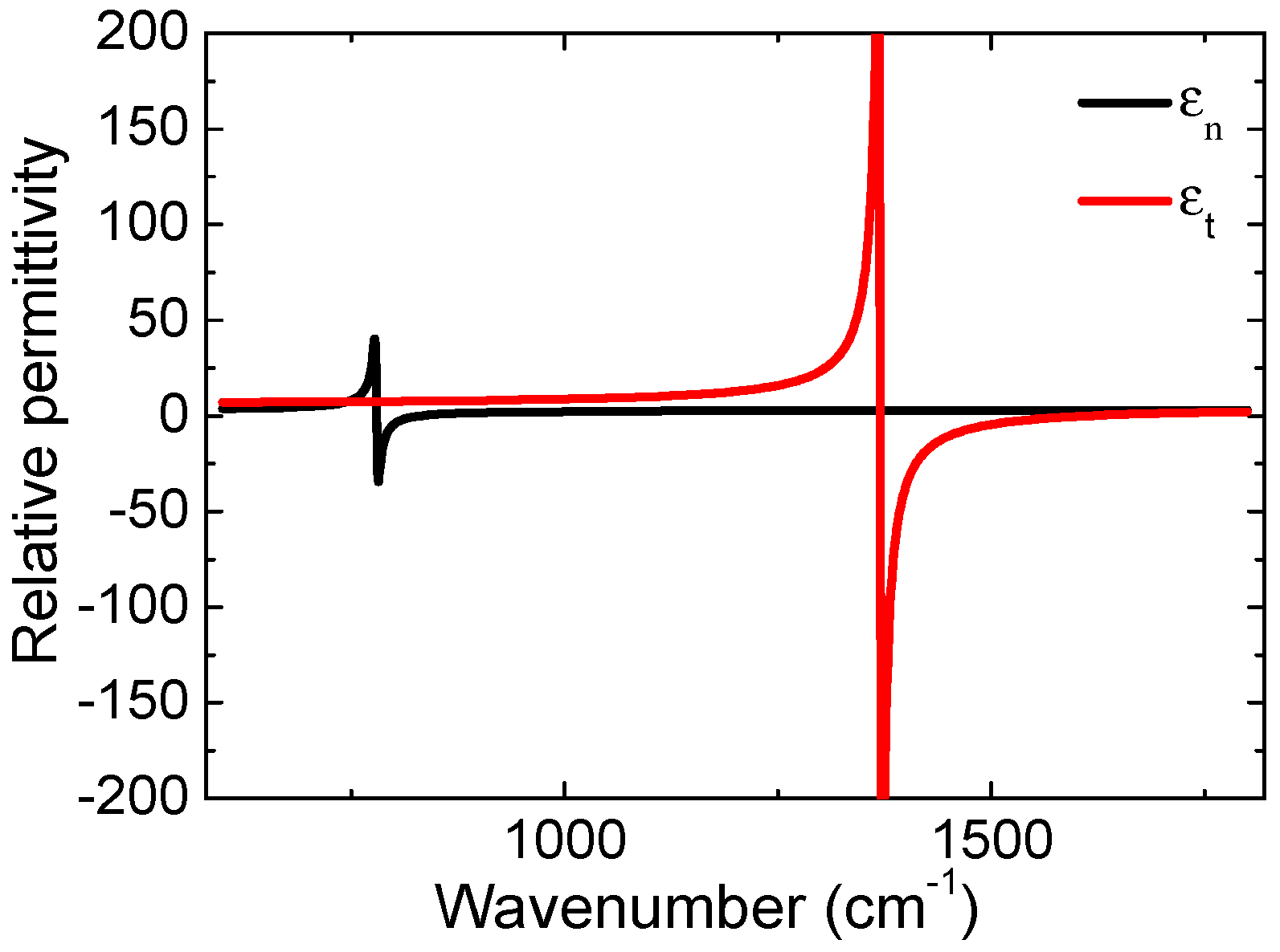
2.1.1. Hexagonal Boron Nitride

h-BN is a hyperbolic material which has two kinds of IR active phonon modes relevant to hyperbolicity: (1) in the normal plane phonon modes, which have ωTO = 780 cm−1, ωLO = 830 cm−1; and (2) in the basal plane phonon modes, which have ωTO = 1370 cm−1, ωLO = 1610 cm−1. These lead to two narrow spectral bandwidths referred to as Reststrahlen (RS) bands which are material-dependent and range bracketed by the longitudinal optic (LO) and transverse optic (TO) phonon frequencies. The lower RS band corresponds to the type-I band (εn < 0, εt > 0), and the upper RS band corresponds to the type-II band (εt < 0, εn > 0). The relative permittivity functions of h-BN in two RS bands is given by [19]
ε n ( t ) = ε , n ( t ) + ε , n ( t ) × ( ω L O , n ( t ) ) 2 ( ω T O , n ( t ) ) 2 ( ω T O , n ( t ) ) 2 ω 2 i ω Γ n ( t )
In addition to ωTO and ωLO mentioned above, the other parameters are the limiting high-frequency permittivities ε , n = 2.95 and ε , t = 4.87 , and the optical phonon broadening Γ n = 4 c m 1 and Γ t = 5 c m 1 . The relation between relative permittivity and wavenumber is shown in Figure 1.

2.1.2. Graphene

In our research, the optical response of graphene is described by conductivity which is modeled utilizing local random phase approximation (local RPA). At T temperature, the conductivity σ of graphene is given by
σ intra = i e 2 k B T π 2 ( ω + i τ g 1 ) ( E F k B T + 2 l n ( e E F k B T + 1 ) )
σ inter = i e 2 4 π ln | 2 E F ( ω + i τ g 1 ) 2 E F + ( ω + i τ g 1 ) |
σ = σ inter + σ intra
where σintra and σinter rely exclusively on intra-band transition contribution and inter-band transition contribution, respectively. The parameter kB is a Boltzmann constant, ℏ is a reduced Plank constant, and EF is the Fermi energy of the graphene. Here, τg is the electron relaxation time. Due to Landau damping already being induced in local RPA, the relaxation time has other contributions: impurity scattering; scattering with phonons (ℏωOPh = 0.2 eV) in graphene and phonon modes of polar substrates; higher-order processes such as phonons coupled to e-h excitations (which have to be treated separately), etc. [26,27,28]. In this work, the relaxation time τg is given by
τ g = μ E F e V F
where μ is the carrier mobility of 10,000 cm2·V−1·s−1 and vF is the Fermi velocity of 106 m/s. According to the derivation above, one can clearly find that the conductivity of graphene depends on its Fermi energy. Moreover, we can tune Fermi energy by applying a gate voltage to control the optical response of graphene.

2.2. Properties of Graphene SPPs and h-BN HPPs

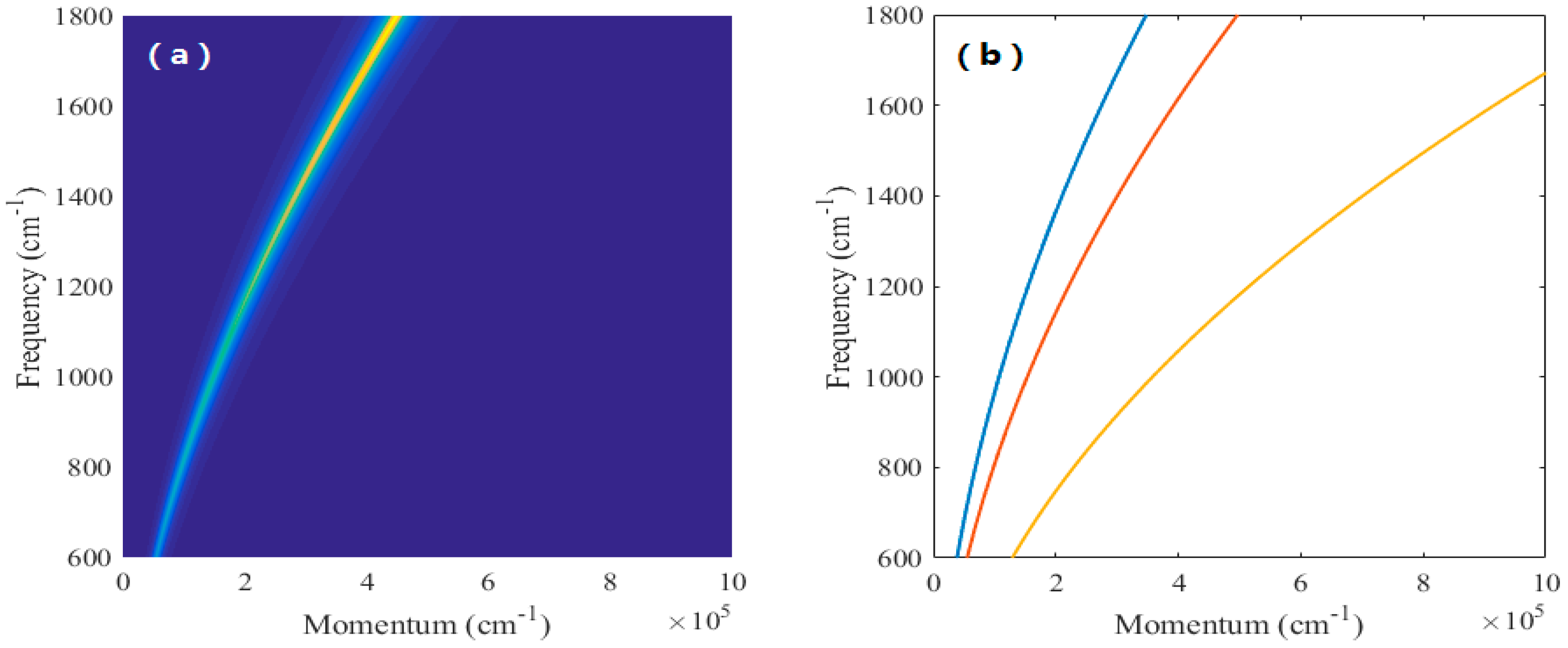
2.2.1. Properties of Graphene SPPs

The properties of graphene SPPs are shown in Figure 2. The transmission property (here, we use a false color map of the imaginary part of the reflectivity r which is controlled by frequency and momentum for visualization) of the freestanding monolayer graphene is clearly shown in Figure 2a with Fermi energy of 0.37 eV which can be easily calculated by employing the standard transfer matrix method (details are shown in part 3). Figure 2b illustrates the frequency/momentum dispersion relation of SPPs modes with Fermi energies of 0.37 eV, 0.17 eV and 0.07 eV. This dispersion is described by
q g r a p h e n e = i ω ε 0 2 π σ ε 0 ( ω ) 2 2 e 2 E F
As shown in Figure 2, one can clearly find that the dispersion curve fits the transmission false color map when Fermi energy is 0.37 eV. This phenomenon can be explained by the energy loss of incident light which is mainly attributed to the excitation of graphene SPPs modes. Moreover, these excited SPPs modes can be controlled by tuning graphene Fermi energy.

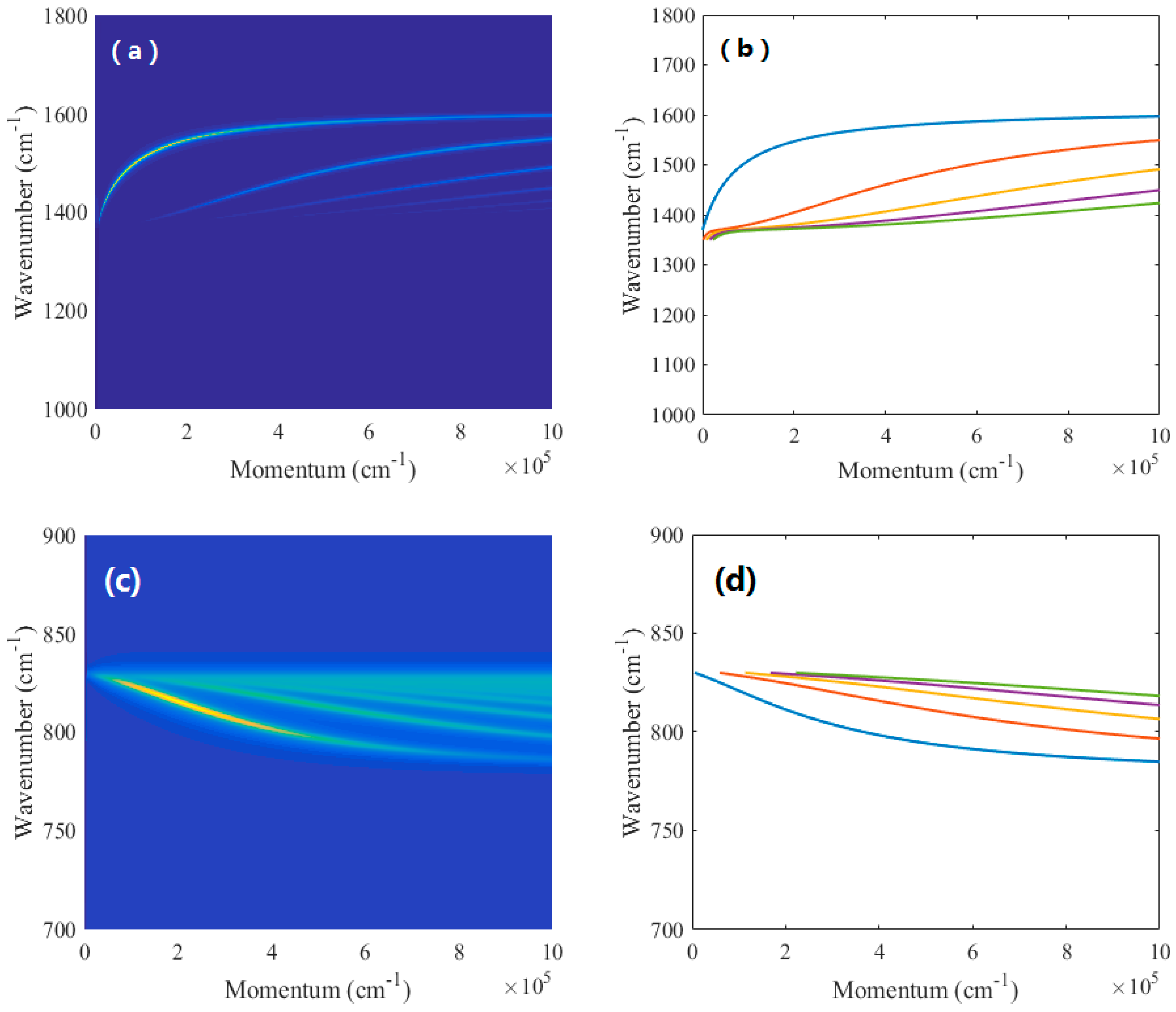
2.2.2. Properties of h-BN HPPs

The analytical approaches of the HPPs properties of h-BN are similar to that of the SPPs properties of graphene. The thickness of h-BN that we choose here is 50 nm. By invoking the quasi-static approximation, the frequency/momentum dispersion is given by
q h B N = ψ d { t a n 1 [ ε 1 ε t ψ ] + t a n 1 [ ε 2 ε t ψ ] + n π }
where ε1 and ε2 are the relative permittivity of mediates above and below h-BN slab, respectively, and ψ = 1 i ( ε n ε t ) , the sign of ψ in the type I band is positive and opposite in the type II band. The parameter n is the order of excitation modes in the two RS bands.
Figure 3 plots the transmission and dispersion of the h-BN slab. One can clearly find that multiple branches of HPP only exist in the two RS bands of h-BN. These different branches correspond to quantized HPP guide modes with a scalar potential that oscillates across the h-BN slab, and these branches have a different number of nodes (0, 1, 2…). Our following research and relevant discussion are aimed at these branches. It is worth mentioning that zero-node does not exist in the type I band compared with the type II band. Furthermore, compared with the false color map in Figure 3a,b, the excitation intensity of the HPP mode is different. This phenomenon expresses that the conversion efficiency of the incident light energy into HPP modes is different in the two RS bands. After discussing the optical properties and response of graphene and h-BN, we then analyze the optical response of different coupling structures by numerical simulation.

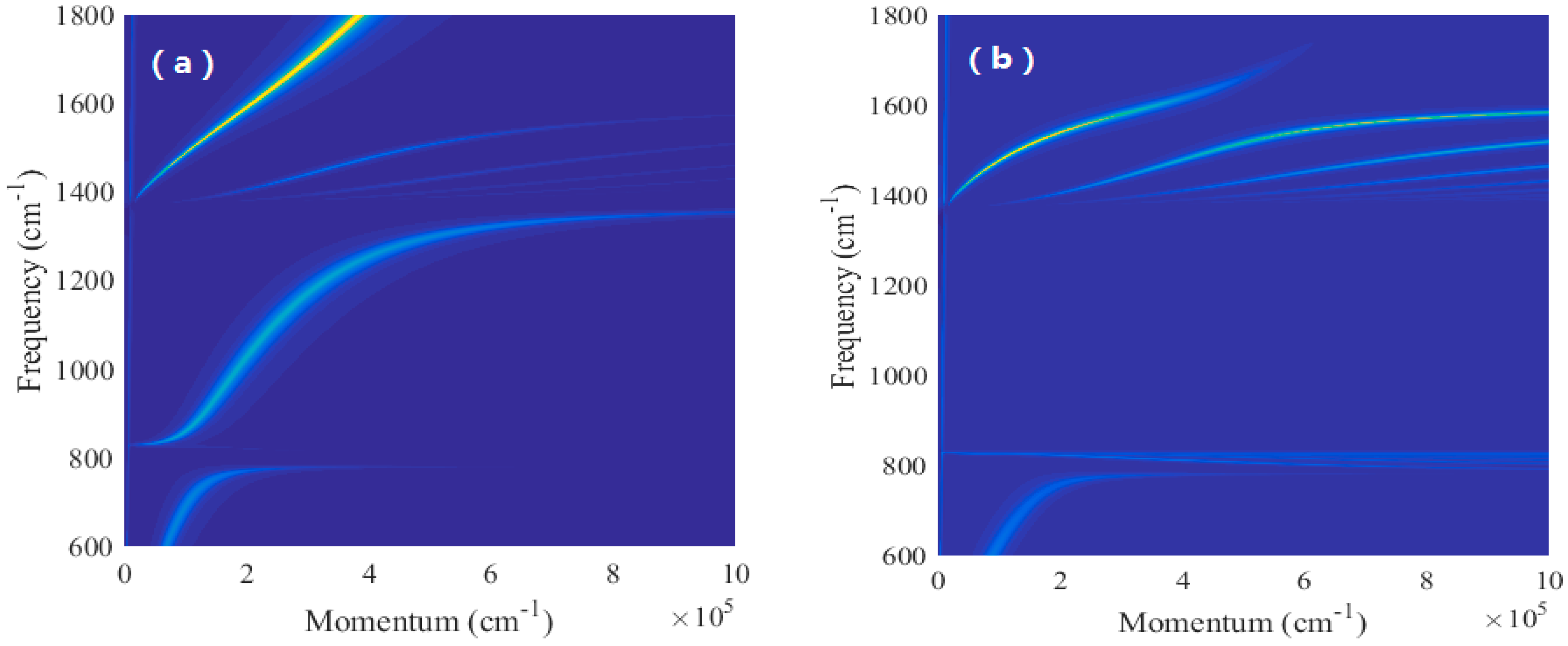
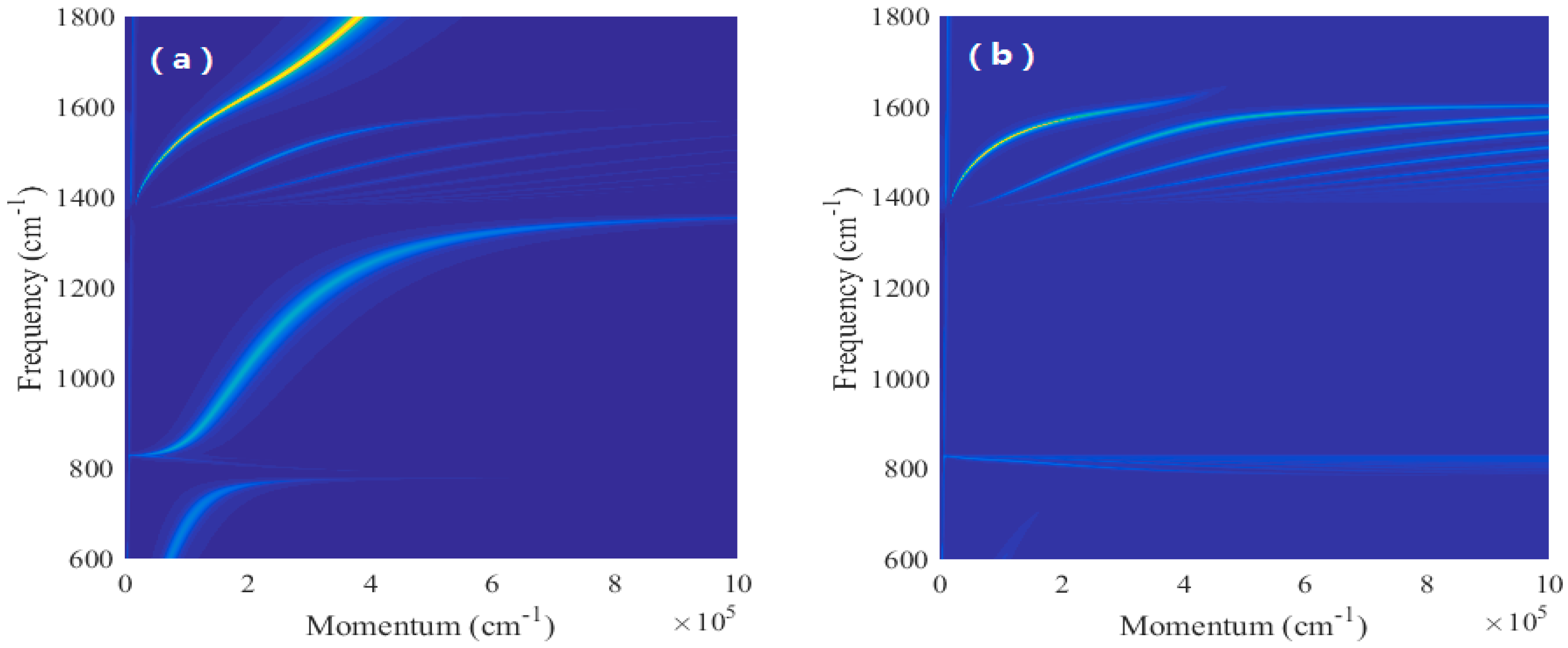
3. Calculation and Results

In this part, we study the optical response and properties of different structures of the graphene–h-BN SPP–HPP coupling system. Firstly, the theoretical models based on different excitation orders are shown in Figure 4. Then, the transmission properties of the models are calculated by employing the standard transfer matrix method.
As shown in Figure 4, the structures of different orders of modes excitation are proposed. Here, an h-BN slab thickness of d is utilized. Due to the thickness of the graphene layer being much smaller than that of other layers, we assume that the graphene layer is used only as a boundary condition. The calculation process in detail is as follows. For the case of P-polarization (TM wave), the out-plane magnetic field in the system is written by
H y = e i k x x ( A j e i k j z z + B j e i k j z z ) k j z = ε j t ( ω 2 c 2 q 2 ε j z )
where the variable j = 0, 1 and 2 stand for the region of the heterostructure system as shown in Figure 4. kjz is the wave vector component along the z axis. εjt and εjz are the permittivity of mediate layers along the x and z axes, respectively. The Air/graphene/h-BN/SiO2 heterostructure, as shown in Figure 4a, consists of the regions: z > 0 (air, j = 0), −d < z < 0 (h-BN, j = 1), and z < −d (SiO2, j = 2). According to the Maxwell equation and boundary conditions, the transfer matrix of the Air/graphene/h-BN interface can be expressed as:
( A 0 B 0 ) = M ( A 2 B 2 ) M = B 01 P 1 B 12
B 01 = 1 2 ( 1 + σ Z 1 + Z 0 Z 1 1 σ Z 1 Z 0 Z 1 1 + σ Z 1 Z 0 Z 1 1 σ Z 1 + Z 0 Z 1 ) P 1 = ( e i k 1 z d 0 0 e i k 1 z d ) B 12 = 1 2 ( 1 + Z 1 Z 2 1 Z 1 Z 2 1 Z 1 Z 2 1 + Z 1 Z 2 )
where B01 and B12 are the transfer matrix of the air/h-BN interface and the h-BN/SiO2 interface, respectively. P1 represents the propagation matrix of the homogeneous dielectric layer—h-BN. The conductivity σ of the graphene layer is given by Equations (2)–(4). Zj is the impedance of material which can be written as
Z j = ω ε j t k j z
In summary, the reflectivity r is equal to M21/M11, where M21 and M11 are the components of the matrix M, which can be calculated as
r = ( 1 + σ Z 1 Z 0 Z 1 ) ( 1 + Z 1 Z 2 ) + ( 1 σ Z 1 + Z 0 Z 1 ) ( 1 Z 1 Z 2 ) e 2 i k 1 z d ( 1 + σ Z 1 + Z 0 Z 1 ) ( 1 + Z 1 Z 2 ) + ( 1 σ Z 1 Z 0 Z 1 ) ( 1 Z 1 Z 2 ) e 2 i k 1 z d
The Air/h-BN/graphene/SiO2 heterostructure, as shown in Figure 4b, consists of regions: z > 0 (air, j = 0), −d < z < 0 (h-BN, j= 1), and j < −d (SiO2, j = 2). In the same way, the transfer matrix of the Air/h-BN interface, homogeneous dielectric layer, h-BN and h-BN/SiO2 interface can be expressed as
B 01 = 1 2 ( 1 + Z 0 Z 1 1 Z 0 Z 1 1 Z 0 Z 1 1 + Z 0 Z 1 ) a = 1 ,   P 1 = ( e i k 1 z d 0 0 e i k 1 z d ) B 12 = 1 2 ( 1 + σ Z 2 + Z 1 Z 2 1 σ Z 2 Z 1 Z 2 1 + σ Z 2 Z 1 Z 2 1 σ Z 2 + Z 1 Z 2 )
For this structure, the reflectivity r’ can be calculated as
r = ( 1 + σ Z 2 + Z 1 Z 2 ) ( 1 Z 0 Z 1 ) + ( 1 + σ Z 2 Z 1 Z 2 ) ( 1 + Z 0 Z 1 ) e 2 i k 1 z d ( 1 + σ Z 2 + Z 1 Z 2 ) ( 1 + Z 0 Z 1 ) + ( 1 + σ Z 2 Z 1 Z 2 ) ( 1 Z 0 Z 1 ) e 2 i k 1 z d
By Comparing Equations (14) and (15), the effects of excitation order on the reflection coefficient are shown in Figure 5. Then, we discuss the tunability of the heterostructure system.
As shown in Figure 5, one can clearly find that the different excitation orders can affect the mode properties in the system. When SPPs are excited first (this situation corresponds to the schematic shown in Figure 4a), SPPs modes play a dominate role in the coupling modes, but HPPs modes occupy a leading position in the case that HPPs are excited first. An interesting phenomenon is that when HPPs are excited first, the coupling mode in the two RS bands disappears. Furthermore, the background color of Figure 5b is lighter than that of Figure 5a. This phenomenon can be explained by utilizing the free-space radiate decay rate that is shown in reference [29]. Subsequently, we discuss the effect of the Fermi energy of graphene on transmission properties.
By comparing Figure 5 with Figure 6, one can clearly find that the frequency of excitation coupling modes is red shifted with the increase of Fermi energy. Finally, we discuss the effect of the thickness of h-BN on transmission properties.
In the same way, we can distinctly find that the frequency of excitation coupling modes is red shifted with the increase of the thickness of h-BN when comparing Figure 6 with Figure 7.
To summarize, the specific derivation process of the transmission properties is demonstrated. Moreover, we also study the tunability of the heterostructure system on several aspects. Some relative discussion is studied as follows.

4. Discussion

4.1. Tunability of the System

In this section, we study some of the details. From the study above, the coupling mode can be tuned by changing the properties of graphene and h-BN. Neglecting the high orders of kx for simplicity, this change in the SPPs’ wavelength induced by graphene is described by
Δ λ λ g r a p h e n e π d ε n 1 ε n ε t
where λgraphene is the corresponding SPPs’ wavelength. This formula clearly shows that the influence of graphene depends on the ratio of SPPs’ wavelength and the thickness of h-BN. Moreover, this clarifies why the effect of graphene remains substantial in h-BN as thick as d = 300 nm [30]. However, Equation (15) seems not to apply the schematic shown in Figure 4b. This can be explained by the intensity of SPPs in graphene excitation which is much lower than HPPs in h-BN when HPPs are excited first. Thus, the tunability of graphene in Figure 4b is weaker than that in Figure 4a.

4.2. The System on Noble Metal

Noble metal is usually used to excite SPPs modes. In this part, we place the heterostructure on a noble metal layer to discuss the coupling modes in brief. The transmission properties are shown in Figure 8.
In contrast to Figure 3 and Figure 4, we can directly find that noble metal has little effect on the coupling modes in Figure 8. This phenomenon is due to the high frequency of the SPPs modes excited by silver; and it is difficult to couple the SPPs modes excited by silver with the HPPs modes excited in h-BN. Thus, it merely makes the excitation frequency of coupling modes in the type II band blue shift.

5. Conclusions

In this work, we have shown that the Van der Waals heterostructures system assembled from monolayer graphene and h-BN slab can provide a method to control light–matter interaction at nanoscale. The features of the coupling modes have been studied based on the dispersion spectrum. The effects of excitation order, Fermi energy of graphene and the thickness of the h-BN slab on the coupling modes have been demonstrated. By tuning the applied voltage, one can easily change the Fermi energy of graphene to control the coupling modes. Furthermore, we also discuss some relative aspects of the coupling modes. Our work is meaningful for both scientific and practical purposes regarding the aspects of efficient subwavelength manipulation of infrared light.

Acknowledgments

This research is supported by the National Natural Science Foundation of China (Grant Nos. 61376099, 61434007 and 61504100) and the Foundation for Fundamental Research of China (Grant No. JSZL2016110B003).

Author Contributions

Hongxia Liu and Shulong Wang developed the concept. Sheng Qu conceived the design. Lu Dong, Lei Wu and Congcong Ma performed the numerical simulations. Hongxia Liu, Shulong Wang and Sheng Qu contributed to writing and finalizing the paper.

Conflicts of Interest

The authors declare no conflict of interest.

References

  1. Naguib, M.; Mashtalir, O.; Carle, J.; Presser, V.; Lu, J.; Hultman, L.; Gogotsi, Y.; Barsoum, M.W. Two-Dimensional Transition Metal Carbides. ACS Nano 2012, 6, 1322–1331. [Google Scholar] [CrossRef] [PubMed]
  2. Xia, F.; Wang, H. Two-dimensional material nanophotonics. Nat. Photonics 2014, 8, 899–907. [Google Scholar] [CrossRef]
  3. Fiori, G.; Bonaccorso, F. Electronics based on two-dimensional materials. Nat. Nanotechnol. 2014, 9, 768–779. [Google Scholar] [CrossRef] [PubMed]
  4. Geim, A.K.; Grigorieva, I.V. Van der Waals heterostructures. Nature 2013, 499, 419–425. [Google Scholar] [CrossRef] [PubMed]
  5. Yang, J.; Wang, Z.; Wang, F.; Xu, R.; Tao, J.; Zhang, S.; Qin, Q.; Luther-Davies, B.; Jagadish, C.; Yu, Z.; et al. Atomically thin optical lenses and gratings. Light Sci. Appl. 2016, 5, e16046. [Google Scholar] [CrossRef]
  6. Li, Y.; Yan, H.; Farmer, D.B.; Meng, X.; Zhu, W.; Osgood, R.M.; Heinz, T.F.; Avouris, P. Graphene plasmon enhanced vibrational sensing of surface-adsorbed layers. Nano Lett. 2014, 14, 1573. [Google Scholar] [CrossRef] [PubMed]
  7. Fang, N.; Lee, H.; Sun, C.; Zhang, X. Sub-diffraction-limited optical imaging with a silver super lens. Science 2005, 308, 534–537. [Google Scholar] [CrossRef] [PubMed]
  8. Chang, D.; Sørensen, A.; Hemmer, P.; Lukin, M. Quantum optics with surface plasmons. Phys. Rev. Lett. 2006, 97, 053002. [Google Scholar] [CrossRef] [PubMed]
  9. Koppens, F.H.L.; Chang, D.E.; Garcia de Abajo, F.J. Graphene Plasmonics: A Platform for Strong Light-Matter Interactions. Nano Lett. 2011, 11, 3370–3377. [Google Scholar] [CrossRef] [PubMed]
  10. Talley, C.E.; Jackson, J.B.; Oubre, C.; Grady, N.K.; Hollars, C.W.; Lane, S.M.; Huser, T.R.; Nordlander, P.; Halas, N.J. Surface-Enhanced Raman Scattering from Individual Au Nanoparticles and Nanoparticle Dimer Substrates. Nano Lett. 2005, 5, 1569–1574. [Google Scholar] [CrossRef] [PubMed]
  11. Yankowitz, M.; Xue, J.; Cormode, D.; Sanchez-Yamagishi, J.D.; Watanabe, K.; Taniguchi, T.; Jarillo-Herrero, P.; Jacquod, P.; LeRoy, B.J. Emergence of superlattice Dirac points in graphene on hexagonal boron nitride. Nat. Phys. 2012, 8, 382–386. [Google Scholar] [CrossRef] [Green Version]
  12. Wang, F.; Zhang, Y.; Tian, C.; Girit, C.; Zettl, A.; Crommie, M.; Shen, Y.R. Gate-variable optical transitions in graphene. Science 2008, 320, 206–209. [Google Scholar] [CrossRef] [PubMed]
  13. Li, Z.Q.; Henriksen, E.A.; Jiang, Z.; Hao, Z.; Martin, M.C.; Kim, P.; Stormer, H.L.; Basov, D.N. Dirac charge dynamics in graphene by infrared spectroscopy. Nat. Phys. 2008, 4, 532–535. [Google Scholar] [CrossRef]
  14. Ju, L.; Geng, B.; Horng, J.; Girit, C.; Martin, M.; Hao, Z.; Bechtel, H.A.; Liang, X.; Zettl, A.; Shen, Y.R.; et al. Graphene plasmonics for tunable terahertz metamaterials. Nat. Nanotechnol. 2011, 6, 630–634. [Google Scholar] [CrossRef] [PubMed]
  15. Chen, J.; Badioli, M.; Alonso-González, P.; Thongrattanasiri, S.; Huth, F.; Osmond, J.; Spasenović, M.; Centeno, A.; Pesquera, A.; Godignon, P. Optical nano-imaging of gate-tunable graphene plasmons. Nature 2012, 487, 77–81. [Google Scholar] [CrossRef] [PubMed]
  16. Fei, Z.; Rodin, A.S.; Andreev, G.O.; Bao, W.; McLeod, S.; Wagner, M.; Zhang, L.M.; Zhao, Z.; Thiemens, M.; Dominguez, G.; et al. Gate-tuning of graphene plasmons revealed by infrared nano-imaging. Nature 2012, 487, 82–85. [Google Scholar] [CrossRef] [PubMed]
  17. Fang, Z.; Wang, Y.; Schlather, A.E.; Liu, Z.; Ajayan, P.M.; de Abajo, F.J.; Nordlander, P.; Zhu, X.; Halas, N.J. Active tunable absorption enhancement with graphene nanodisk arrays. Nano Lett. 2014, 14, 299–304. [Google Scholar] [CrossRef] [PubMed]
  18. Li, L.H.; Chen, Y. Atomically Thin Boron Nitride: Unique Properties and Applications. Adv. Funct. Mater. 2016, 26, 2594–2608. [Google Scholar] [CrossRef]
  19. Dai, S.; Fei, Z.; Ma, Q.; Rodin, A.S.; Wagner, M.; McLeod, A.S.; Liu, M.K.; Gannett, W.; Regan, W.; Watanabe, K.; et al. Tunable Phonon Polaritons in Atomically Thin van der Waals Crystals of Boron Nitride. Science 2014, 343, 1125–1129. [Google Scholar] [CrossRef] [PubMed]
  20. Dai, S.; Ma, Q.; Andersen, T.; Mcleod, A.S.; Fei, Z.; Liu, M.K.; Wagner, M.; Watanabe, K.; Taniguchi, T.; Thiemens, M.; et al. Sub diffractional focusing and guiding of polaritonic rays in a natural hyperbolic material. Nat. Commun. 2015, 6, 6963. [Google Scholar] [CrossRef] [PubMed]
  21. Guo, Y.; Newman, W.; Cortes, C.L.; Jacob, Z. Applications of hyperbolic metamaterial substrates. Adv. Optoelectron. 2012, 2012, 452502. [Google Scholar] [CrossRef]
  22. Poddubny, A.; Iorsh, I.; Belov, P.; Kivshar, Y. Hyperbolic metamaterials. Nat. Photonics 2013, 7, 948–957. [Google Scholar] [CrossRef]
  23. Caldwell, J.D.; Kretinin, A.V.; Kretinin, A.; Chen, Y.; Giannini, V.; Fogler, M.M.; Francescato, Y.; Ellis, C.T.; Tischler, J.G.; Woods, C.R.; et al. Sub-diffractional volume-confined polaritons in the natural hyperbolic material hexagonal boron nitride. Nat. Commun. 2014, 5, 5221. [Google Scholar] [CrossRef] [PubMed]
  24. Brar, V.W.; Jang, M.S.; Sherrott, M.; Kim, S.; Lopez, J.J.; Kim, L.B.; Choi, M.; Atwater, H. Hybrid surface-phonon–plasmon polariton modes in graphene/monolayer h-BN heterostructures. Nano Lett. 2014, 14, 3876–3880. [Google Scholar] [CrossRef] [PubMed]
  25. Xu, X.G.; Jiang, J.H.; Gilburd, L.; Rensing, R.G.; Burch, K.S.; Zhi, C.; Bando, Y.; Golberg, D.; Walker, G.C. Mid-infrared polaritonic coupling between boron nitride nanotubes and graphene. ACS Nano 2014, 8, 11305–11312. [Google Scholar] [CrossRef] [PubMed]
  26. Woessner, A.; Lundeberg, M.B.; Gao, Y.; Principi, A.; Alonso-González, P.; Carrega, M.; Watanabe, K.; Taniguchi, T.; Vignale, G.; Polini, M.; et al. Highly confined low-loss plasmons in graphene–boron nitride heterostructures. Nat. Mater. 2015, 14, 421–425. [Google Scholar] [CrossRef] [PubMed]
  27. Yan, H.; Low, T.; Zhu, W.; Wu, Y.; Freitag, M.; Li, X.F.; Avouris, P.; Xia, F. Damping pathways of mid-infrared plasmons in graphene nanostructures. Nat. Photonics 2013, 7, 394–399. [Google Scholar] [CrossRef]
  28. Jablan, M.; Soljacic, M.; Buljan, H. Plasmons in Graphene: Fundamental Properties and Potential Applications. IEEE 2013, 101, 1689–1704. [Google Scholar] [CrossRef]
  29. Krishnamoorthy, H.N.S.; Jacob, Z.; Narimanov, E.; Kretzschmar, I.; Menon, V.M. Topological transitions in metamaterials. Science 2012, 336, 1–2. [Google Scholar] [CrossRef] [PubMed]
  30. Dai, S.; Ma, Q.; Liu, M.K.; Andersen, T.; Fei, Z.; Goldflam, M.D.; Wagner, M.; Watanabe, K.; Taniguchi, T.; Thiemens, M.; et al. Graphene on hexagonal boron nitride as a tunable hyperbolic metamaterial. Nat. Nanotechnol. 2015, 10, 682–686. [Google Scholar] [CrossRef] [PubMed]
Figure 1. Relative permittivity of h-BN, which clearly shows the hyperbolicity in the two RS bands.
Crystals 07 00049 g001
Figure 2. (a) Calculated transmission of freestanding monolayer graphene. (b) Calculated dispersion of freestanding monolayer graphene with Fermi energies of 0.5 eV (blue line), 0.35 eV (red line) and 0.15 eV (yellow line).
Crystals 07 00049 g002
Figure 3. (a,b) Calculated transmission and dispersion of the freestanding h-BN slab near the type I band. (c,d) Calculated transmission and dispersion of the freestanding h-BN slab near the type II band.
Crystals 07 00049 g003
Figure 4. Schematic of the coupling mode in our calculation, (a) SPPs excited first (b) HPPs excited first. Monolayer graphene is located on h-BN (a) and in the center of the h-BN and substrate (b). We assume that these 2D structures are infinite in the xy-plane. Here, the substrate we use is SiO2.
Crystals 07 00049 g004
Figure 5. The effect of different excitation orders on transmission properties. (a) SPPs excited first and (b) HPPs excited first. Here, the Fermi energy of graphene and the thickness of the h-BN slab are 0.5 eV and 50 nm, respectively.
Crystals 07 00049 g005
Figure 6. The effect of the Fermi energy of graphene on transmission properties. (a) SPPs excited first and (b) HPPs excited first. Here, the Fermi energy of graphene and the thickness of the h-BN slab are 0.8 eV and 50 nm, respectively.
Crystals 07 00049 g006
Figure 7. The effect of different excitation orders on transmission properties. (a) SPPs excited first and (b) HPPs excited first. Here, the Fermi energy of graphene and the thickness of the h-BN slab are 0.8 eV and 100 nm, respectively.
Crystals 07 00049 g007
Figure 8. The transmission properties of (a) air/h-BN/Ag/SiO2 heterostructure and (b) air/graphene/h-BN/Ag/SiO2 heterostructure. Here, the thickness of the h-BN slab and silver slab are 50 nm and 10 nm, respectively. The Fermi energy of graphene is 0.5 eV.
Crystals 07 00049 g008

