
Indium Substitution Effect on the Topological Crystalline Insulator Family (Pb1−xSnx)1−yInyTe: Topological and Superconducting Properties

 , and
, and 
Abstract
:1. Introduction
2. Results
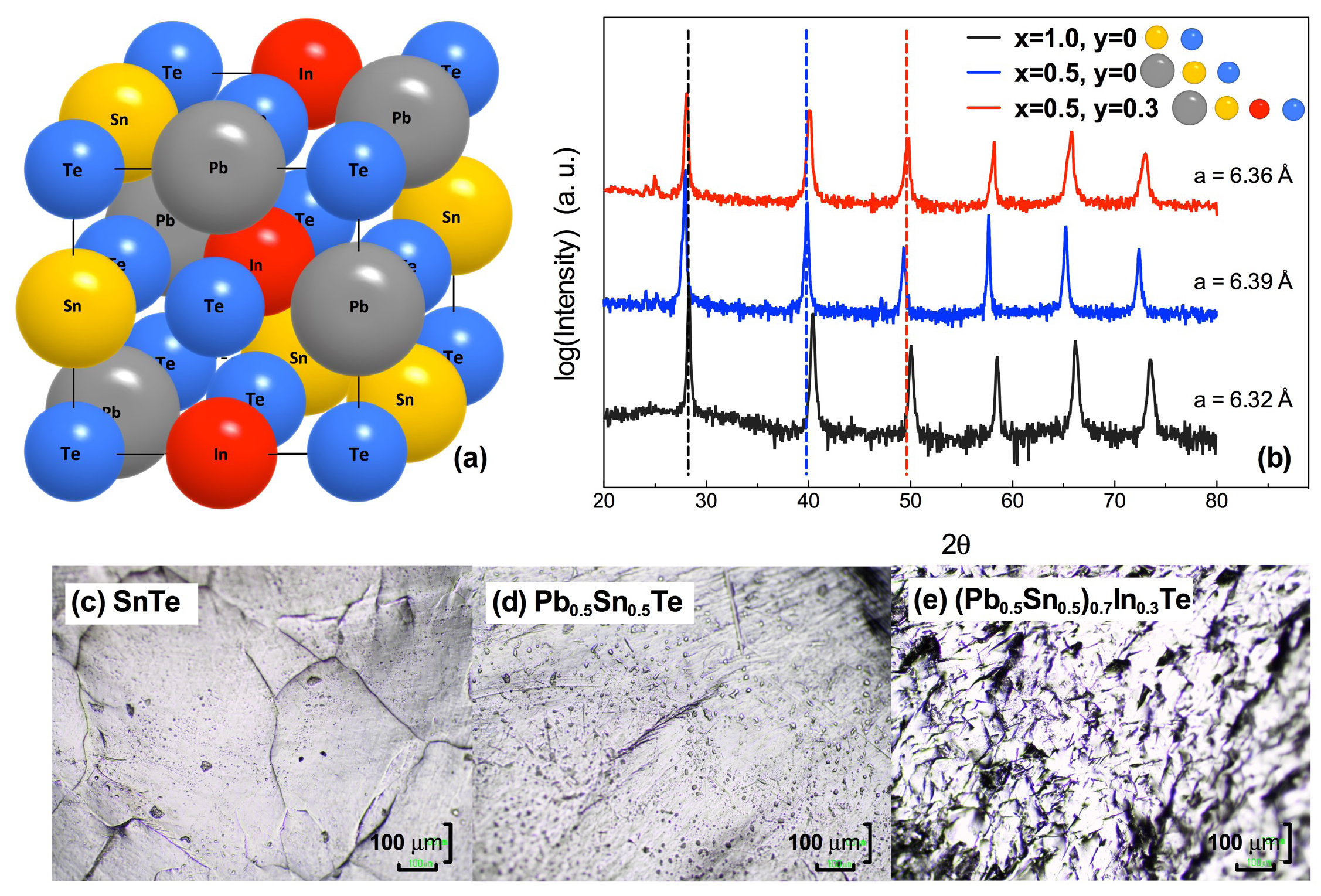
2.1. Crystal Structure
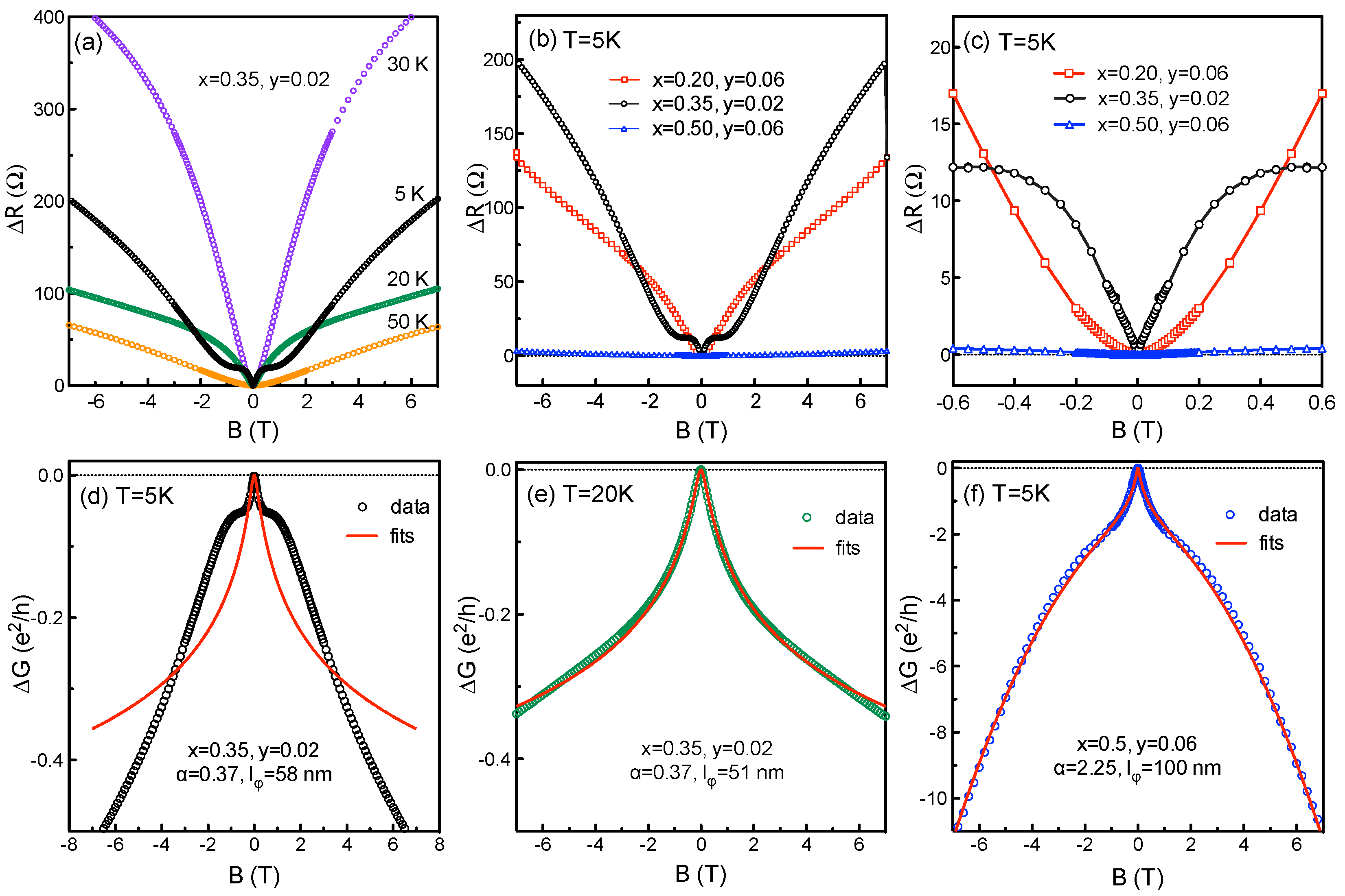
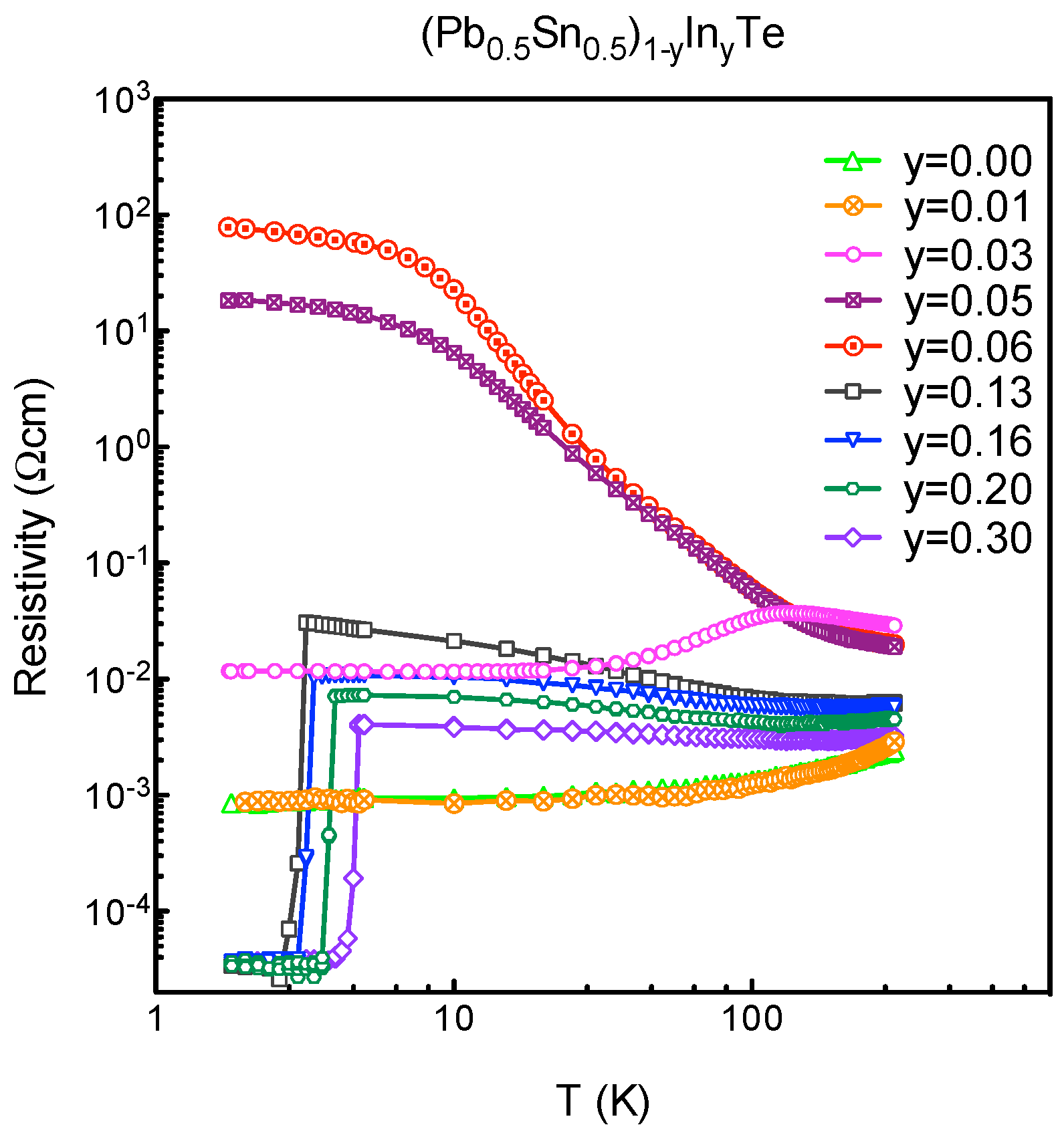
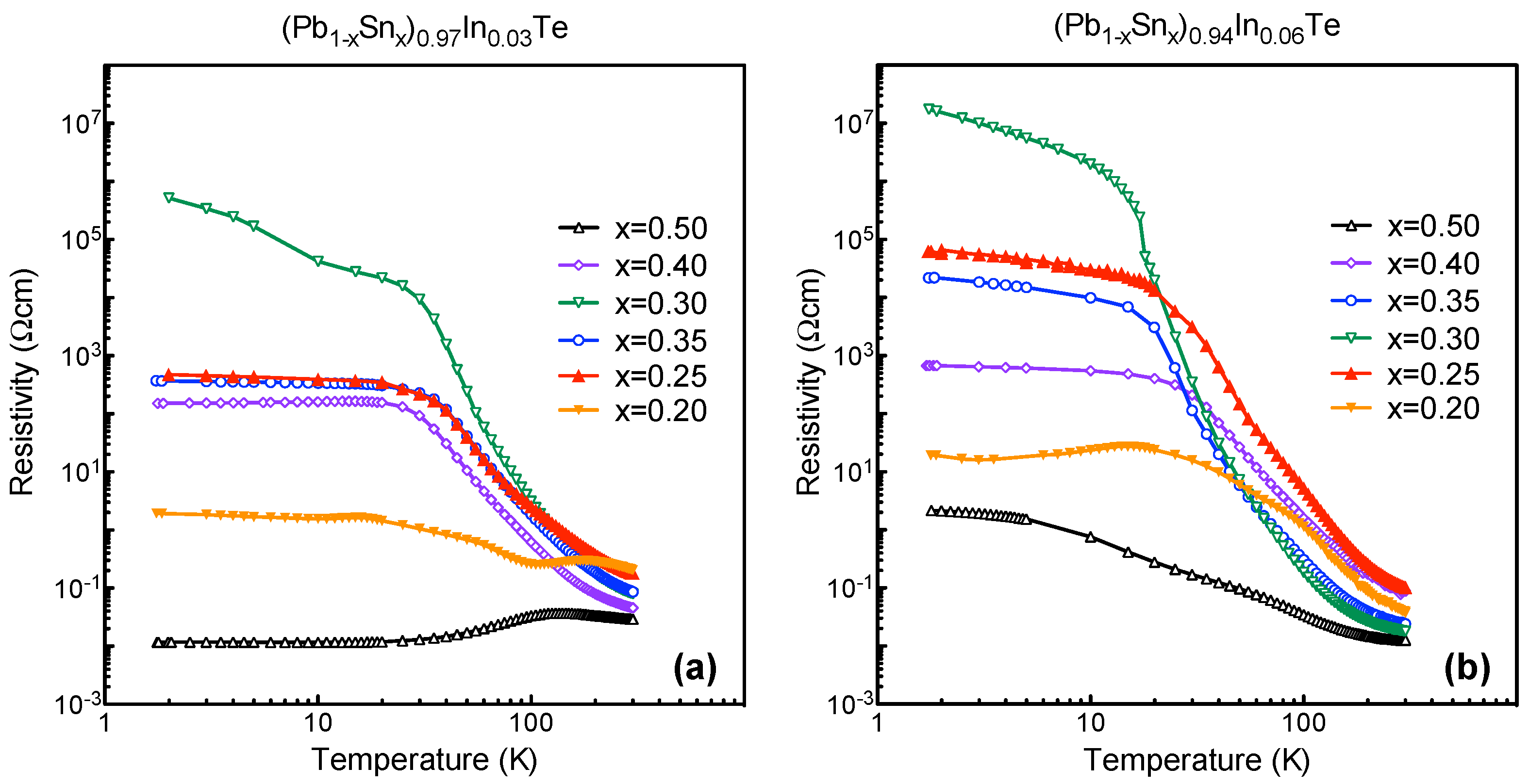
2.2. Resistivity Behaviors of In-Doped Te
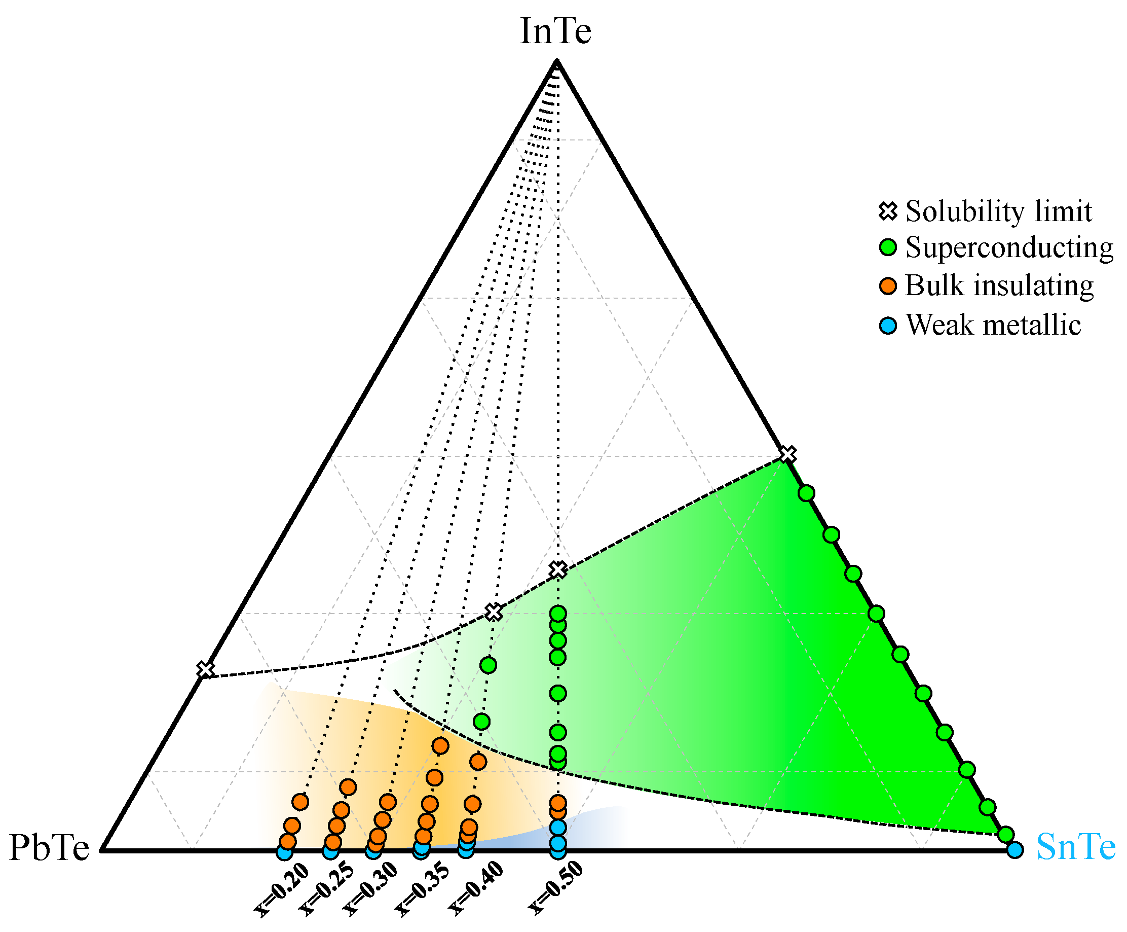
2.3. Phase Diagram
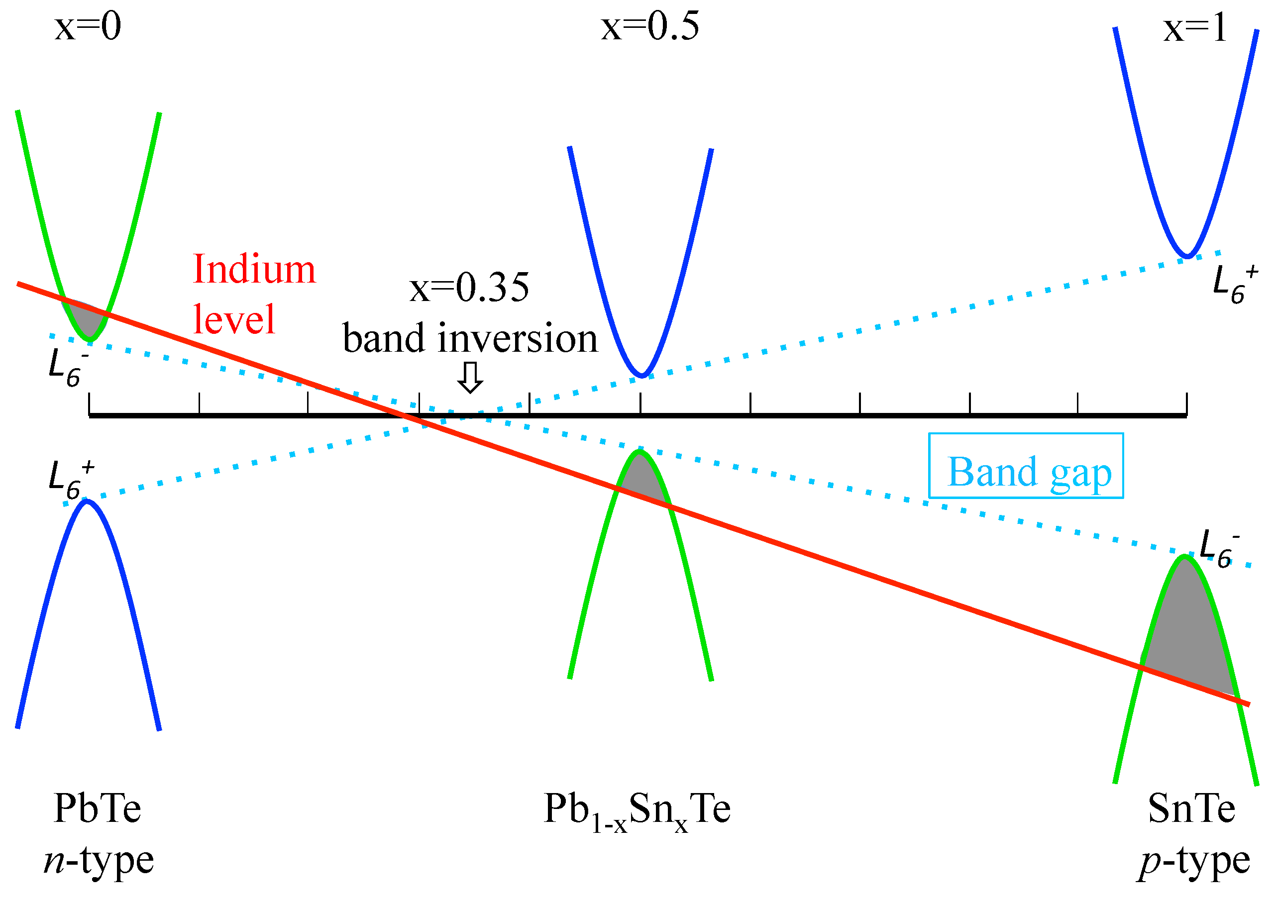
2.4. Bulk Band Structure
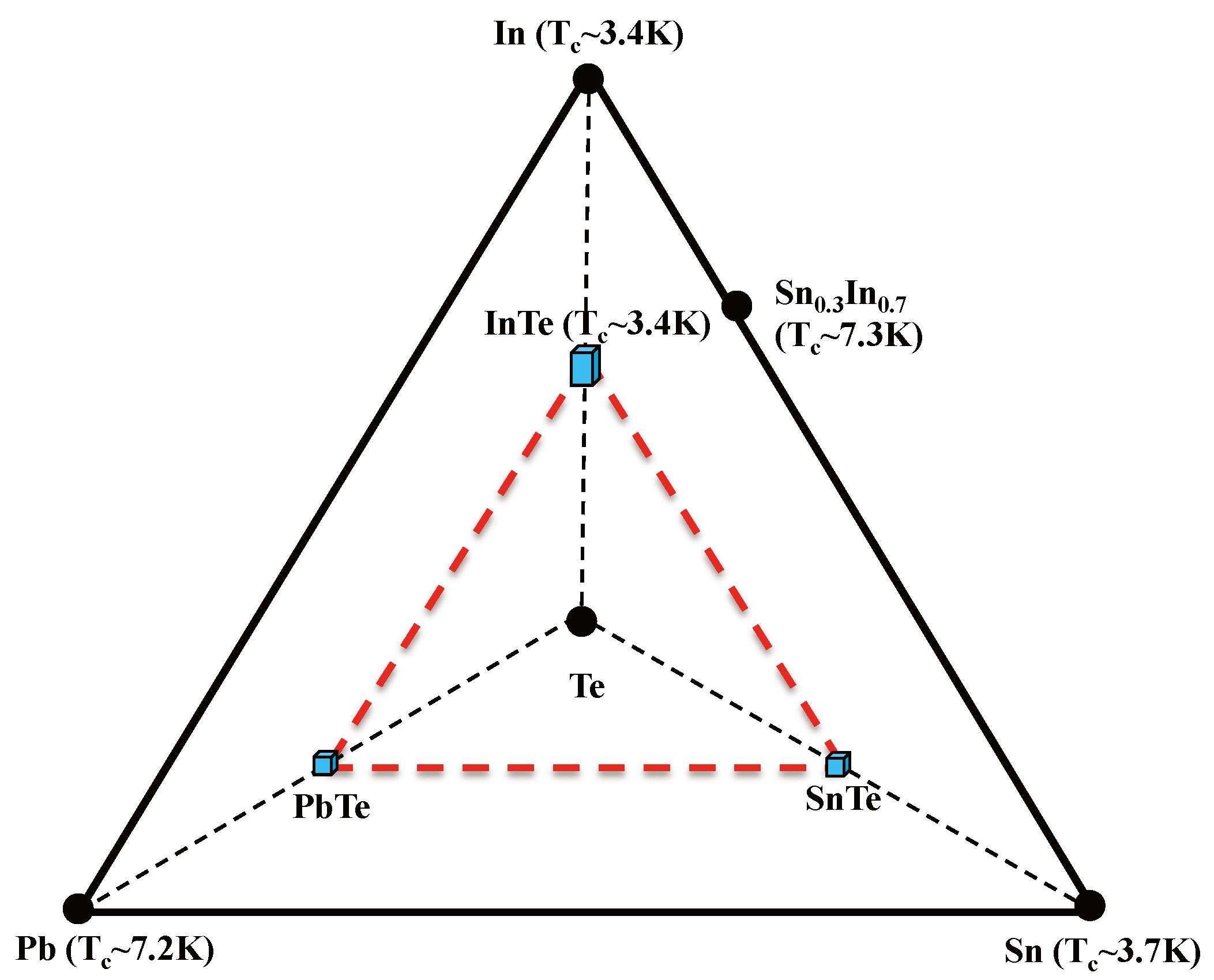
2.5. Debate on Topological Superconductivity
3. Discussion
4. Experimental Section
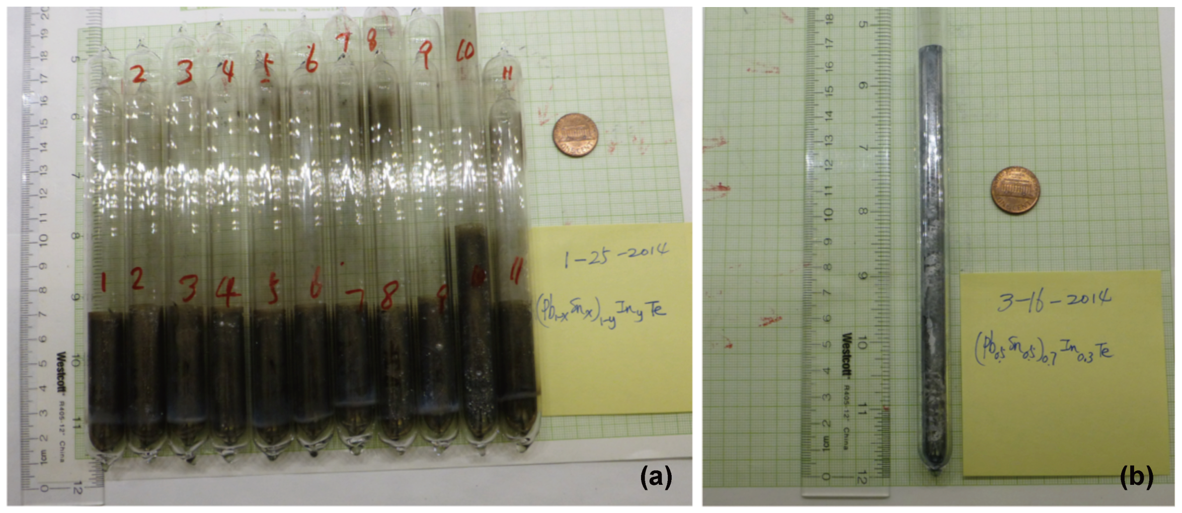
4.1. Sample Preparation
4.2. Sample Characterizations
Acknowledgments
Author Contributions
Conflicts of Interest
Abbreviations
| TI | Topological insulators |
| SOC | spin–orbit coupling |
| ARPES | angle-resolved photoemission spectroscopy |
| TCI | topological crystalline insulator |
| TSC | topological superconductors |
| SIT | SnInTe |
| PSIT | (PbSn)InTe |
| STM | scanning tunneling microscopy |
| MR | magnetoresistance |
| WAL | weak anti-localization |
| TSFZ | traveling-solvent floating-zone |
| EDS | energy-dispersive X-ray spectroscopy |
| CFN | Center for Functional Nanomaterials |
| MPMS | Magnetic Property Measurement System |
| SQUID | Superconducting Quantum Interference Device |
References
- Hasan, M.Z.; Kane, C.L. Colloquium: Topological insulators. Rev. Mod. Phys. 2010, 82, 3045. [Google Scholar] [CrossRef]
- Qi, X.-L.; Zhang, S.-C. Topological insulators and superconductors. Rev. Mod. Phys. 2011, 83, 1057. [Google Scholar] [CrossRef]
- Ando, Y. Topological insulator materials. J. Phys. Soc. Jpn. 2013, 82, 102001. [Google Scholar] [CrossRef]
- Charles, K.; Joel, M. Topological insulators. Phys. World 2011, 24, 32. [Google Scholar]
- Fu, L.; Kane, C.L.; Mele, E.J. Topological insulators in three dimensions. Phys. Rev. Lett. 2007, 98, 106803. [Google Scholar] [CrossRef] [PubMed]
- Bernevig, B.A.; Hughes, T.L.; Zhang, S.C. Quantum spin Hall effect and topological phase transition in HgTe quantum wells. Science 2006, 314, 1757. [Google Scholar] [CrossRef] [PubMed]
- Hsieh, D.; Qian, D.; Wray, L.; Xia, Y.; Hor, S.; Cava, R.J.; Hasan, M.Z. A topological Dirac insulator in a quantum spin Hall phase. Nature 2008, 454, 970. [Google Scholar] [CrossRef] [PubMed]
- Zhang, H.; Liu, C.-X.; Qi, X.-L.; Dai, X.; Fang, Z.; Zhang, S.-C. Topological insulators in Bi2Se3, Bi2Te3 and Sb2Te3 with a single Dirac cone on the surface. Nat. Phys. 2009, 5, 438. [Google Scholar] [CrossRef]
- Xia, Y.; Qian, D.; Hsieh, D.; Wray, L.; Pal, A.; Bansil, A.; Grauer, D.; Hor, Y.S.; Cava, R.J.; Hasan, M.Z. Observation of a large-gap topological-insulator class with a single Dirac cone on the surface. Nat. Phys. 2009, 5, 398. [Google Scholar] [CrossRef]
- Chen, Y.L.; Analytis, J.G.; Chu, J.-H.; Liu, Z.K.; Mo, S.-K.; Qi, X.L.; Zhang, H.J.; Lu, D.H.; Dai, X.; Fang, Z.; et al. Experimental realization of a three-dimensional topological insulator, Bi2Te3. Science 2009, 325, 178. [Google Scholar] [CrossRef] [PubMed]
- Fu, L. Topological crystalline insulators. Phys. Rev. Lett. 2011, 106, 106802. [Google Scholar] [CrossRef] [PubMed]
- Hsieh, T.H.; Lin, H.; Liu, J.; Duan, W.; Bansil, A.; Fu, L. Topological crystalline insulators in the SnTe material class. Nat. Commun. 2012, 3, 982. [Google Scholar] [CrossRef] [PubMed] [Green Version]
- Tanaka, Y.; Ren, Z.; Sato, T.; Nakayama, K.; Souma, S.; Takahashi, T.; Segawa, K.; Ando, Y. Experimental realization of a topological crystalline insulator in SnTe. Nat. Phys. 2012, 8, 800. [Google Scholar] [CrossRef]
- Dziawa, P.; Kowalski, B.J.; Dybko, K.; Buczko, R.; Szczerbakow, A.; Szot, M.; Łusakowska, E.; Balasubramanian, T.; Wojek, B.M.; Berntsen, M.H.; et al. Topological crystalline insulator states in PbxSnxSe. Nat. Mater. 2012, 11, 1023. [Google Scholar] [PubMed]
- Xu, S.-Y.; Liu, C.; Alidoust, N.; Neupane, M.; Qian, D.; Belopolski, I.; Denlinger, J.D.; Wang, Y.J.; Lin, H.; Wray, L.A.; et al. Observation of a topological crystalline insulator phase and topological pahse transition in Pb1−xSnxTe. Nat. Commun. 2012, 3, 1192. [Google Scholar] [CrossRef] [PubMed]
- Yan, C.; Liu, J.; Zang, Y.; Wang, J.; Wang, Z.; Wang, P.; Zhang, Z.; Wang, L.; Ma, X.; Ji, S.; et al. Experimental observation of Dirac-like surface states and topological phase transition in Pb1−xSnxTe(111) films. Phys. Rev. Lett. 2014, 112, 186801. [Google Scholar] [CrossRef] [PubMed]
- Sun, Y.; Zhong, Z.; Shirakawa, T.; Franchini, C.; Li, D.; Li, Y.; Yunoki, S.; Chen, X. Rocksalt SnS and SnSe: Native topological crystalline insulators. Phys. Rev. B 2013, 88, 235122. [Google Scholar] [CrossRef]
- Barone, P.; Rauch, T.; Sante, D.; Henk, J.; Mertig, I.; Picozzi, S. Pressure-induced topological phase transitions in rocksalt chalcogenides. Phys. Rev. B 2013, 88, 045297. [Google Scholar] [CrossRef]
- Hsieh, T.H.; Liu, J.; Fu, L. Topological crystalline insulators and Dirac octets in antiperovskites. Phys. Rev. B 2014, 90, 081112(R). [Google Scholar] [CrossRef]
- Munoz, F.; Vergniory, M.G.; Rauch, T.; Henk, J.; Chulkov, E.V.; Mertig, I.; Botti, S.; Marques, M.A.L.; Romero, A.H. Topological crystalline insulator in a new Bi semiconducting phase. Sci. Rep. 2016, 6, 21790. [Google Scholar] [CrossRef] [PubMed]
- Fu, L.; Berg, E. Odd-parity topological superconductors: Theory and application to CuxBi2Se3. Phys. Rev. Lett. 2010, 105, 097001. [Google Scholar] [CrossRef] [PubMed]
- Hor, Y.S.; Williams, A.J.; Checkelsky, J.G.; Roushan, P.; Seo, J.; Xu, Q.; Zandbergen, H.W.; Yazdani, A.; Ong, N.P.; Cava, R.J. Superconductivity in CuxBi2Se3 and its implications for pairing in the undoped topological insulator. Phys. Rev. Lett. 2010, 104, 057001. [Google Scholar] [CrossRef] [PubMed]
- Sato, T.; Tanaka, Y.; Nakayama, K.; Souma, S.; Takahashi, T.; Sasaki, S.; Ren, Z.; Taskin, A.A.; Segawa, K.; Ando, Y. Fermiology of the strongly spin-orbit coupled superconductor Sn1−xInxTe: Implications for topological superconductivity. Phys. Rev. Lett. 2013, 110, 206804. [Google Scholar] [CrossRef] [PubMed]
- Erickson, A.S.; Chu, J.-H.; Toney, M.F.; Geballe, T.H.; Fisher, I.R. Enhanced superconducting pairing interaction in indium-doped tin telluride. Phys. Rev. B 2009, 79, 024520. [Google Scholar] [CrossRef]
- Balakrishnan, G.; Bawden, L.; Cavendish, S.; Lees, M.R. Superconducting properties of the In-substituted topological crystalline insulator SnTe. Phys. Rev. B 2013, 87, 140507(R). [Google Scholar] [CrossRef]
- Zhong, R.D.; Schneeloch, J.A.; Shi, X.Y.; Xu, Z.J.; Zhang, C.; Tranquada, J.M.; Li, Q.; Gu, G.D. Optimizing the superconducting transition temperature and upper critical field of Sn1−xInxTe. Phys. Rev. B 2013, 88, 020505(R). [Google Scholar] [CrossRef]
- Novak, M.; Sasaki, S.; Kriener, M.; Segawa, K.; Ando, Y. Unusual nature of fully gapped superconductivity in In-doped SnTe. Phys. Rev. B 2013, 88, 140502(R). [Google Scholar] [CrossRef]
- Zhong, R.D.; Schneeloch, J.A.; Liu, T.S.; Camino, F.E.; Tranquada, J.M.; Gu, G.D. Superconductivity induced by In substitution into the topological crystalline insulator Pb0.5Sn0.5Te. Phys. Rev. B 2014, 90, 020505(R). [Google Scholar] [CrossRef]
- Skinner, B.; Chen, T.; Shklovskii, B.I. Why is the bulk resistivity of topological insulators so small? Phys. Rev. Lett. 2012, 109, 176801. [Google Scholar] [CrossRef] [PubMed]
- Butch, N.P.; Kirshenbaum, K.; Syers, P.; Sushkov, A.B.; Jenkins, G.S.; Drew, H.D.; Paglione, J. Strong surface scattering in ultrahigh-mobility Bi2Se3. Phys. Rev. B 2010, 81, 241301(R). [Google Scholar] [CrossRef]
- Jia, S.; Ji, H.; Climent-Pascual, E.; Fuccillo, M.K.; Charles, M.E.; Xiong, J.; Ong, N.P.; Cava, R.J. Low-carrier-concentration crystals of the topological insulator Bi2Te2Se. Phys. Rev. B 2011, 84, 235206. [Google Scholar] [CrossRef]
- Peng, H.; Lai, K.; Kong, D.; Meister, S.; Chen, Y.; Qi, X.; Zhang, S.; Shen, Z.; Cui, Y. Aharonov-Bohm interference in topological insulator nanoribbons. Nat. Mater. 2011, 9, 225. [Google Scholar] [CrossRef] [PubMed]
- Hor, Y.S.; Richardella, A.; Roushan, P.; Xia, Y.; Checkelsky, J.G.; Yazdani, A.; Hasan, M.Z.; Ong, N.P.; Cava, R.J. p-type Bi2Se3 for topological insulator and low-temperature thermoelectric applicaitons. Phys. Rev. B 2009, 79, 195208. [Google Scholar] [CrossRef]
- Analytis, J.G.; McDonald, R.D.; Riggs, S.C.; Chu, J.; Boebinger, G.S.; Fisher, I.R. Two-dimensional surface state in the quantum limit of a topological insulator. Nat. Phys. 2010, 6, 960. [Google Scholar] [CrossRef]
- Checkelsky, J.G.; Hor, Y.S.; Cava, R.J.; Ong, N.P. Bulk band gap and surface state conduction obsered in voltage-tuned crystals of the topological insulator Bi2Se3. Phys. Rev. Lett. 20011, 106, 196801. [Google Scholar] [CrossRef] [PubMed]
- Zhong, R.; He, X.; Schneeloch, J.A.; Zhang, C.; Liu, T.; Pletikosić, I.; Yilmaz, T.; Sinkovic, B.; Li, Q.; Ku, W.; et al. Surface-state-dominated transport in crystals of the topological crystalline insulator In-doped Pb1−xSnxTe. Phys. Rev. B 2015, 91, 195321. [Google Scholar] [CrossRef]
- Villars, P. Pauling File. In Inorganic Solid Phases; Springer: Heidelberg, Germany, 1998; Volume 41C, pp. 1–8. [Google Scholar]
- Haldolaarachchige, N.; Gibson, Q.; Xie, W.; Nielsen, M.B.; Kushwaha, S.; Cava, R.J. Anomalous composition dependence of the superconductivity in In-doped SnTe. Phys. Rev. B 2016, 93, 024520. [Google Scholar] [CrossRef]
- Du, G.; Du, Z.; Fang, D.; Yang, H.; Zhong, R.D.; Schneeloch, J.; Gu, G.D.; Wen, H. Fully gapped superconductivity in In-doped topological crystalline insulator Pb0.5Sn0.5Te. Phys. Rev. B 2015, 92, 020512(R). [Google Scholar] [CrossRef]
- Dixon, J.R.; Bis, R.F. Band inversion and the electrical properties of PbxSn1−xTe. Phys. Rev. 1968, 176, 942. [Google Scholar] [CrossRef]
- Vul, B.M.; Voronova, I.D.; Kalyuzhnaya, G.A.; Mamedov, T.S.; Ragimova, T.S. Characteristics of transfer phenomena in Pb0.78Sn0.22Te with a large indium content. Phys. Rev. Lett. 1966, 26, 1193. [Google Scholar]
- Kozub, V.I.; Parfen’ev, R.V.; Shamshur, D.V.; Shakura, D.V.; Chernyaev, A.V.; Nemov, S.A. Superconductor-insulator transition in (Pb1−zSnz)0.84In0.16Te. JETP Lett. 1979, 29, 18. [Google Scholar]
- Shamshur, D.V.; Nemov, S.A.; Parfen’ev, R.V.; Kononchuk, M.S.; Nizhankovskii, V.I. Low-temperature conductivity and the Hall effect in (Pb1−zSnz)0.84In0.16Te semiconducting solid solutions. Phys. Solid State 2008, 50, 2028. [Google Scholar] [CrossRef]
- Bansal, N.; Kim, Y.; Brahlek, M.; Edrey, E.; Oh, S. Thickness-independent transport channels in topological insulator Bi2S33 thin films. Phys. Rev. Lett. 2012, 109, 116804. [Google Scholar] [CrossRef] [PubMed]
- Serbyn, M.; Fu, L. Symmetry breaking and Landau quantization in topological crystalline insulators. Phys. Rev. B 2014, 90, 035402. [Google Scholar] [CrossRef]
- Akiyama, R.; Fujisawa, K.; Sakurai, R.; Kuroda, S. Weak antilocalization in (111) thin films of a topological crystalline insulator SnTe. J. Phys. Conf. Ser. 2014, 568, 052001. [Google Scholar] [CrossRef]
- Kim, Y.S.; Brahlek, M.; Bansal, N.; Edrey, E.; Kapilevich, G.A.; Iida, K.; Tanimura, M.; Horibe, Y.; Cheong, S.-W.; Oh, S. Thickness-dependent bulk properties and weak antilocalization effect in topological insulator Bi2Se3. Phys. Rev. B 2011, 84, 073109. [Google Scholar] [CrossRef]
- Hikami, S.; Larkin, A.I.; Nagaoka, Y. Spin-Orbit Interaction and Magnetoresistance in the Two Dimensional Random System. Prog. Theor. Phys. 1980, 63, 707. [Google Scholar] [CrossRef]
- Assaf, B.A.; Katmis, F.; Wei, P.; Satpati, B.; Zhang, Z.; Bennett, S.P.; Harris, V.G.; Moodera, J.S.; Heiman, D. Quantum coherent transport in SnTe topological crystalline insulator thin films. Appl. Phys. Lett. 2014, 105, 102108. [Google Scholar] [CrossRef]
- Kushwaha, S.K.; Pletikosić, I.; Liang, T.; Gyenis, A.; Lapidus, S.H.; Tian, Y.; Zhao, H.; Burch, K.S.; Lin, J.; Wang, W.; et al. Sn-doped Bi1.1Sb0.9Te2S bulk crystal topological insulator with excellent properties. Nat. Commun. 2016, 7, 11456. [Google Scholar] [CrossRef] [PubMed]
- Ravich, Y.I.; Nemov, S.A. Hopping conduction via strongly localized impurity states of indium in PbTe and its solid solutions. Semiconductors 2002, 36, 1–20. [Google Scholar] [CrossRef]
- Kaĭdanov, V.I.; Ravich, Y.I. Deep and resonance states in AIVBVI semiconductors. Sov. Phys. Usp. 1985, 28, 31–53. [Google Scholar]
- Pankratov, O.A.; Pakhomov, S.V.; Volkov, B.A. Supersymmetry in heterojuctions: Band-inverting contact on the basis of Pb1−xSnxTe and Hg1-xCdxTe. Solid State Commun. 1987, 61, 93–96. [Google Scholar] [CrossRef]
- Dimmock, J.O.; Melngailis, I.; Strauss, A.J. Band structure and laser action in PbxSn1−xTe. Phys. Rev. Lett. 1966, 26, 1193. [Google Scholar] [CrossRef]
- Gao, X.; Daw, M.S. Investigation of band inversion in (Pb,Sn)Te alloys using abinitio calculations. Phys. Rev. B 2008, 77, 033103. [Google Scholar] [CrossRef]
- Tanaka, Y.; Sato, T.; Nakayama, K.; Souma, S.; Takahashi, T.; Ren, Z.; Novak, M.; Segawa, K.; Ando, Y. Tunability of the k-space location of the dirac cones in the topological crystalline insulator Pb1−xSnxTe. Phys. Rev. B 2013, 87, 155105. [Google Scholar] [CrossRef]
- Zhang, Q.; Liao, B.; Lan, Y.; Lukas, K.; Liu, W.; Esfarjani, K.; Opeil, C.; Broido, D.; Chen, G.; Ren, Z. High thermoelectric performance by resonant dopant indium in nanostructured SnTe. Proc. Natl. Acad. Sci. USA 2013, 110, 13261. [Google Scholar] [CrossRef] [PubMed]
- Bushmarina, G.S.; Drabkin, I.A.; Mashovets, D.V.; Parfeniev, R.V.; Shamshur, D.V.; Shachov, M.A. Superconducting properties of the SnTe-PbTe system doped with indium. Phys. B Condens. Matter 1991, 169, 687. [Google Scholar] [CrossRef]
- Heremans, J.P.; Wiendlocha, B.; Chamoire, M. Resonant levels in bulk thermoelectric semiconductors. Energy Environ. Sci. 2012, 5, 5510. [Google Scholar] [CrossRef]
- Maeda, S.; Katsube, S.; Zheng, G. Quasi-localized impurity state in doped topological crystalline insulator Sn0.9In0.1Te probed by 125Te-NMR. J. Phys. Soc. Jpn. 2017, 86, 024702. [Google Scholar] [CrossRef]
- Qi, X.; Hughes, T.L.; Raghu, S.; Zhang, S. Time-reversal invariant topological superconductors and superfluids in two and three dimensions. Phys. Rev. Lett. 2009, 102, 187001. [Google Scholar] [CrossRef] [PubMed]
- Qi, X.; Hughes, T.L.; Raghu, S.; Zhang, S. Topological invariants for the Fermi surface of a time-reversal- invariant superconductor. Phys. Rev. B 2010, 81, 134508. [Google Scholar] [CrossRef]
- Sasaki, S.; Kriener, M.; Segawa, K.; Yada, K.; Tanaka, Y.; Sato, M.; Ando, Y. Topological superconductivity in CuxBi2Se3. Phys. Rev. Lett. 2011, 107, 217001. [Google Scholar] [CrossRef] [PubMed]
- Kirzhner, T.; Lahoud, E.; Chaska, K.B.; Salman, Z.; Kanigel, A. Point-contact spectroscopy of Cu0.2Bi2Se3 single crystals. Phys. Rev. B 2012, 86, 064517. [Google Scholar] [CrossRef]
- Sasaki, S.; Ren, Z.; Taskin, A.A.; Segawa, K.; Fu, L.; Ando, Y. Odd-parity pairing and topological superconductivity in a strongly spin-orbit coupled semiconductor. Phys. Rev. Lett. 2012, 109, 217004. [Google Scholar] [CrossRef] [PubMed]
- Levy, N.; Zhang, T.; Ha, J.; Sharifi, F.; Talin, A.A.; Kuk, Y.; Stroscio, J.A. Experimental evidence for s-wave pairing symmetry in superconducting CuxBi2Se3 single crystals using a scanning tunneling microscope. Phys. Rev. Lett. 2013, 110, 117001. [Google Scholar] [CrossRef] [PubMed]
- He, L.P.; Zhang, Z.; Pan, J.; Hong, X.C.; Zhou, S.Y.; Li, S.Y. Fully superconducting gap in the doped topological crystalline insulator Sn0.6In0.4Te. Phys. Rev. B 2013, 88, 014523. [Google Scholar] [CrossRef]
- Saghir, M.; Barker, J.A.T.; Balakrishnan, G.; Hillier, A.D.; Lees, M.R. Superconducting properties of Sn1−xInxTe (x=0.38-0.45) studied using muon-spin spectroscopy. Phys. Rev. B 2014, 90, 064508. [Google Scholar] [CrossRef]
- Matano, K.; Kriener, M.; Segawa, K.; Ando, Y.; Zheng, G. Spin-rotation symmetry breaking in the superconducting state of CuxBi2Se3. Nat. Phys. 2016, 12, 852. [Google Scholar] [CrossRef]
- Arpino, K.E.; Wallace, D.C.; Nie, Y.F.; Birol, T.; King, P.D.C.; Chatterjee, S.; Uchida, M.; Koohpayeh, S.M.; Wen, J.-J.; Page, K.; et al. Evidence for topologically protected surface states and a superconducting phase in [Tl4](Tl1−xSnx)Te3. Phys. Rev. Lett. 2014, 112, 017002. [Google Scholar] [CrossRef] [PubMed]
- Arpino, K.E.; Wasser, B.D.; McQueen, T.M. Superconducting dome and crossover to an insulating state in [Tl4]Tl1−xSnxTe3. APL Mater. 2015, 3, 041507. [Google Scholar] [CrossRef]
- Liang, F.; Kane, C.L. Superconducting proximity effect and Majorana fermions at the surface of a topological insulator. Phys. Rev. Lett. 2008, 100, 096407. [Google Scholar]
- Wang, M.; Liu, C.; Xu, J.; Yang, F.; Miao, L.; Yao, M.; Gao, C.L.; Shen, C.; Ma, X.; Chen, X.; et al. The coexistence of superconductivity and topological order in the Bi2Se3 thin films. Science 2012, 336, 52. [Google Scholar] [CrossRef] [PubMed]
- Wang, E.; Ding, H.; Fedorov, A.V.; Yao, W.; Li, Z.; Lv, Y.; Zhao, K.; Zhang, L.; Xu, Z.; Schneeloch, J.; et al. Fully gapped topological surface states in Bi2Se3 films induced by a d-wave high-temperature superconductor. Nat. Phys. 2013, 9, 621. [Google Scholar] [CrossRef]
- Xu, J.; Liu, C.; Wang, M.; Ge, J.; Liu, Z.; Yang, X.; Chen, Y.; Liu, Y.; Xu, Z.; Gao, C.; et al. Artificial topological superconductor by the proximity effect. Phys. Rev. Lett. 2014, 112, 217001. [Google Scholar] [CrossRef]
- Li, Z.; Zhang, F.; Wang, Q. Majorana modes in a topological insulator/s-wave superconductor heterostructure. Sci. Rep. 2014, 4, 6363. [Google Scholar] [CrossRef] [PubMed]
- Xu, J.; Wang, M.; Liu, Z.; Ge, J.; Yang, X.; Liu, C.; Xu, Z.; Guan, D.; Gao, C.; Qian, D.; et al. Experimental detection of a Majorana mode in the core of a magnetic vortex inside a topological insulator-superconductor Bi2Te3/NbSe2 heterostructure. Phys. Rev. Lett. 2015, 114, 017001. [Google Scholar] [CrossRef] [PubMed]


© 2017 by the authors. Licensee MDPI, Basel, Switzerland. This article is an open access article distributed under the terms and conditions of the Creative Commons Attribution (CC BY) license ( http://creativecommons.org/licenses/by/4.0/).
Share and Cite
Zhong, R.; Schneeloch, J.; Li, Q.; Ku, W.; Tranquada, J.; Gu, G. Indium Substitution Effect on the Topological Crystalline Insulator Family (Pb1−xSnx)1−yInyTe: Topological and Superconducting Properties. Crystals 2017, 7, 55. https://doi.org/10.3390/cryst7020055
Zhong R, Schneeloch J, Li Q, Ku W, Tranquada J, Gu G. Indium Substitution Effect on the Topological Crystalline Insulator Family (Pb1−xSnx)1−yInyTe: Topological and Superconducting Properties. Crystals. 2017; 7(2):55. https://doi.org/10.3390/cryst7020055
Chicago/Turabian StyleZhong, Ruidan, John Schneeloch, Qiang Li, Wei Ku, John Tranquada, and Genda Gu. 2017. "Indium Substitution Effect on the Topological Crystalline Insulator Family (Pb1−xSnx)1−yInyTe: Topological and Superconducting Properties" Crystals 7, no. 2: 55. https://doi.org/10.3390/cryst7020055