
Material and Device Architecture Engineering Toward High Performance Two-Dimensional (2D) Photodetectors

1
Department of Physics, School of Science, Beijing Jiaotong University, No. 3 Shang Yuan Cun, Hai Dian District, Beijing 100044, China
2
Tianjin Key Laboratory of Molecular Optoelectronic Sciences, Department of Chemistry, Tianjin University, Tianjin 300072, China
3
Collaborative Innovation Center of Chemical Science and Engineering, Tianjin 300072, China
4
Key Laboratory of Luminescence and Optical Information, Ministry of Education, School of Science, Beijing Jiaotong University, Beijing 100044, China
*
Authors to whom correspondence should be addressed.
Crystals 2017, 7(5), 149; https://doi.org/10.3390/cryst7050149
Submission received: 1 April 2017
/
Revised: 4 May 2017
/
Accepted: 10 May 2017
/
Published: 22 May 2017
(This article belongs to the Special Issue Two-Dimensional Materials beyond Graphene and their Van der Waals Heterostructures)
Abstract
:Photodetectors based on two-dimensional (2D) nanostructures have led to a high optical response, and a long photocarrier lifetime because of spatial confinement effects. Since the discovery of graphene, many different 2D semiconductors have been developed and utilized in the ultrafast and ultrasensitive detection of light in the ultraviolet, visible, infrared and terahertz frequency ranges. This review presents a comprehensive summary of recent breakthroughs in constructing high-performance photodetectors based on 2D materials. First, we give a general overview of 2D photodetectors based on various single-component materials and their operating wavelength (ultraviolet to terahertz regime). Then, we summarize the design and controllable synthesis of heterostructure material systems to promote device photoresponse. Subsequently, special emphasis is put on the accepted methods in rational engineering of device architectures toward the photoresponse improvements. Finally, we conclude with our personal viewpoints on the challenges and promising future directions in this research field.
1. Introduction
The photodetector, as one of the most important optoelectronic devices in modern society, has demonstrated the ability to precisely transform light into electrical signals. Such accurate detections of light in the ultraviolet (UV), visible (vis), infrared (IR) and terahertz (THz) frequency ranges is contributed by various semiconducting bandgaps, which are of fundamental and practical importance for applications in industrial, medical and environmental research. With developments in nanoscience and nanoengineering, numerous nanomaterials based on different semiconductors have been synthesized for photodetectors [1]. The optoelectronic properties of photodetection systems can be fine-tuned and modulated by varying individual structural parameters, including shape, size and surface morphology [2].
Among various types of nanostructured materials, two-dimensional (2D) materials have been considered as potential candidates for high-performance photodetectors [3,4], because of their high crystal quality features and rich physical properties. For instance, simply adjusting the number of semiconductor layers could lead to a tunable bandgap, which helps to design photodetectors for an exact working wavelength. Moreover, the thin planar materials with ultra-smooth surfaces are highly compatible with flexible substrates, which are ideal building blocks for fabrication of flexible photodetectors. Up to now, various 2D semiconducting materials have already been fabricated with wide selections of light detection spanning from the UV to THz regime [5,6,7]. However, an inherent limitation of 2D semiconductors is that they are still restricted in fulfilling so-called “5S” requirements (high sensitivity, high signal-to-noise ratio, high spectral selectivity, high speed, and high stability) for practical applications.
In atomically thin semiconductors, the limited optical absorption cross section leads to weak photocurrent generation, and thus reverses the photosensitivity. For example, the low level of optical absorption in conventional graphene phototransistors induces relatively poor responsivity (~10−2 A W−1) [8]. Consequently, significant efforts have been devoted to investigations of the inherent properties of 2D materials [9,10,11], which help to provide guidance for designing and exploring new 2D nanomaterials with a better light absorptivity and longer carrier diffusion length. Moreover, graphene as a versatile 2D material has shed new light on developing novel 2D photodetectors. Besides exploring new materials, heterojunction material systems have provided an alternative platform to promote photoresponse performance. Such 2D heterojunction photodetectors may benefit from the combined properties from each individual semiconductor [12,13,14] and the internal field in the heterojunctions [15,16], which could induce effective separations of the photo-generated electron/hole pairs. In addition to artificially modulating these material systems, device structure engineering is another strategy to reduce contact resistance, which effectively applies the gate voltage or form-effective Schottky barriers between semiconductors and electrodes.
Material system design and device architecture engineering play the key roles in optimizing photoresponse performances. To provide a comprehensive design guideline of 2D photodetectors, this paper reviews the current breakthroughs in the field of high-performance photodetectors based on 2D materials. We first screen the available 2D photodetectors based on various single-component materials and present their operating wavelengths, from UV to THz frequency regions. Then, the state-of-the-art of photodetectors is discussed based on the 2D heterojunction material systems. Furthermore, a tailored construction of 2D devices and novel nanotechnologies are demonstrated for photoresponse improvement. Finally, we discuss the possible challenges and opportunities in the future development of photodetectors.
2. Two-dimensional Photodetectors Made of Single-Component Semiconductors
The performance of photodetectors is determined by the ability to transform optical signals into electrical signals. This complex process is mainly dependent on the inherent characteristics of the photodetector’s active materials, such as absorption coefficient, lifetime of electron-hole pair and charge mobility. Several types of materials are selected and designed to satisfy the specific photoresponse, including graphene, transition metal dichalcogenides (TMDs) [17] (MoS2, WS2, MoSe2), IIIA–VIA group [18,19] (GaS, GaSe, InSe, In2Se3), IVA–VIA group compounds [20] (SnS2), black phosphorus and the recently discovered all-inorganic perovskites [21,22].
As an example, graphene, a single layer of carbon atoms arranged in a hexagonal lattice, is an appealing material for photonics and electronics [23,24,25]. Conventional graphene materials can absorb photons from visible to infrared range [26,27] and exhibit a huge electrical mobility up to 200,000 cm2 V−1 s−1 for a free sheet for both electrons and holes [28], which promote ultrafast conversion of photons or plasmons [29] to electrical currents or voltages for photo response. However, the high dark current arising from the gapless nature of graphene significantly reduces the sensitivity of photodetection [30,31] and restricts further developments of graphene-based photodetectors. The discovery of 2D transition metal dichalcogenides (TMDs) with direct energy gaps in the near-infrared (NIR) to the visible spectral regions [32,33] has opened up a new window for photodetector fabrication [34]. Besides TMDs, group IIIA–VIA layered semiconductors have gained interest due to their anisotropic optical, electronic, and mechanical properties. The multilayer phototransistor based on IIIA–VIA semiconductors has reached a photoresponsivity value higher than 104 AW−1 and the photoresponse time is only about 6 ms [35], which is one of the fastest among the reported layered material photodetectors.
Another class of 2D materials (VA–VIA), topological insulators [36], normally have a very small band gap (0.15~0.3 eV) in the mid-infrared range [37]. The small band gap of those 2D materials allows for detections of near-infrared wavelengths and telecommunication band. Being earth-abundant, the IVA–VIA layered materials are particularly desirable for sustainable optoelectronic devices [38]. As a 2D semiconducting material, the IVA–VIA group materials have unique crystal structures, in which weak van der Waals forces between adjacent layers contribute to form stacked layers, allowing formation of stable thin crystals with thickness down to a few atomic layers. Even a monolayered and bilayered IVA–VIA compound has been successfully fabricated recently [39]. Those high-quality thin single-crystalline layered materials based on IVA–VIA semiconductors have showed remarkable performance of high responsivity and fast response rates.
Layered group VII-transition metal dichalcogenides are also a typical class of 2D materials that exhibit a wide range of new physical phenomena. Unlike other 2D-TMDs, those layer materials have an extra electron in the d orbital, which leads to significantly different bandgap properties, distinct quantum confinement effects, and weak interlayer coupling. The corresponding photodetectors exhibit competitive device performance [40]. Moreover, black phosphorus (BP) with a layer-dependent direct band gap from monolayer to bulk has become an emerging material for photodetection [41,42,43,44,45], which exhibits good optoelectronics characteristics over a wide spectrum ranging from UV to NIR. Lately, one kind of new 2D materials, halide perovskites, has been revealed as a very promising material for photodetectors [46] due to their fascinating features, such as large light absorption coefficients [47], broad absorption range, [48] and high carrier mobility [49].
Multi-layered semiconductor materials perform distinct photoelectronic properties, which have been rapidly established as intriguing building blocks for 2D photodetectors. Table 1 summarizes their inherent properties, corresponding to the crystals structures and device performance of single-component semiconductors. Although each type of material has unique characteristics, efforts are still needed to overcome many intrinsic weaknesses. The approaches, including tailoring material systems and rationally designing device structures, will be thoroughly discussed in the following sections.
3. Heterojunction Material Systems for High Performance 2D Photodetectors
Other than single junction photodetectors, the heterojunction 2D structured materials can be fabricated through van der Waals interactions [66,67]. Heterojunction material systems can not only combine advantages from each material [68,69], but also allow for the modulation of band structures for photoresponse improvements [12]. Two-dimensional heterostructures can be classified into two main species (graphene-based and hybrid semiconductor materials) based on the material composition and physical principles.
3.1. Graphene-Based Heterojunctions
Researchers have found that responsivity of graphene-based photodetectors is greatly increased due to their extraordinary electrical and optical properties. However, the gapless nature of intrinsic graphene and the limited light absorption in each atomic layer prevent efficient photocarrier separation in graphene photodetectors. To overcome this shortcoming, the integration of graphene with other materials appears to be a promising approach [70,71], such as quantum dots/graphene [72,73], MoS2/graphene [12], WSe2/graphene [71] and Bi2Te3/graphene [74] heterojunctions. One easy and functional approach for fabrication of these heterojunctions is by reattaching the different films onto each other [12]. This multiple transferring procedure may bring contaminations to the interfaces, which would limit the practical applications. Epitaxial growth of 2D material directly onto other material layers is an alternate approach for fabricating such heterostructures [75,76], which enables a guarantee of the quality of the material systems. Photodetectors based on those 2D graphene-based heterojunctions have achieved unprecedented high responsivity and sensitivity because of the synergistic effects. In those systems, the graphene layers are applicable for broadband, ultrafast technologies, whereas the other semiconductors are suitable for applications requiring strong light absorption and electroluminescence.
A novel hybrid graphene-quantum dot phototransistor has been fabricated by Gerasimos Konstantatos et al. [77], as shown in Figure 1a. Because of the strongly light-absorbing and spectrally tunable colloidal quantum dots, the responsivity of this hybrid photodetector is as high as ~5 × 10⁷ AW−1 at low excitation power and the photocurrent response obviously follows the absorption of the PbS quantum dots (Figure 1b). This work demonstrates that efficient electronic coupling of graphene with other technologies such as light absorbing materials will open pathways for high performance photodetectors.
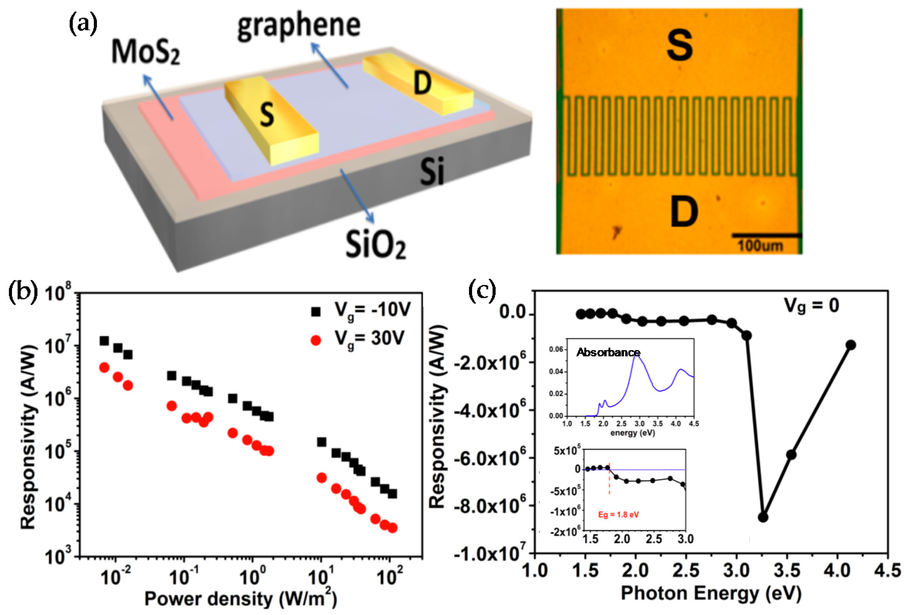
As a typical TMD material, MoS2 has shown reasonably high photoresponsivity ranging from 7.5 mA W−1 to 780 A W−1 under ambient conditions. The bandgap of MoS2 can be tuned by varying the number of layers in crystal structure. A tunable direct band gap would provide great flexibility for designing devices with a wide spectrum response. Figure 2a shows a schematic view of a photodetector based on a graphene-on-MoS2 heterostructure, proposed by Wenjing Zhang et al. [12]. It is worth noting that the photoresponsivity of this device reaches 1.2 × 10⁷ A W−1 (at Vg = −10 V; Vds = 1 V; light power density ~0.01 W m−2) as shown in Figure 2b. The dependence of photoresponsivity of the graphene/MoS2 heterojunction on the wavelength of light at room temperature is shown in Figure 2c, which implies photoresponsivity is induced when the excitation energy is higher than the absorption band gap of MoS2 (1.8 eV), which is consistent with the optical absorption feature of MoS2 layer (Figure 2c inset). It suggests that the photocurrent, generated in this system, originates from light absorption in MoS2. This novel 2D heterostructure material exceeds the capacities of its constituents, providing a valuable reference for optoelectronic applications based on various heterostructural 2D materials.
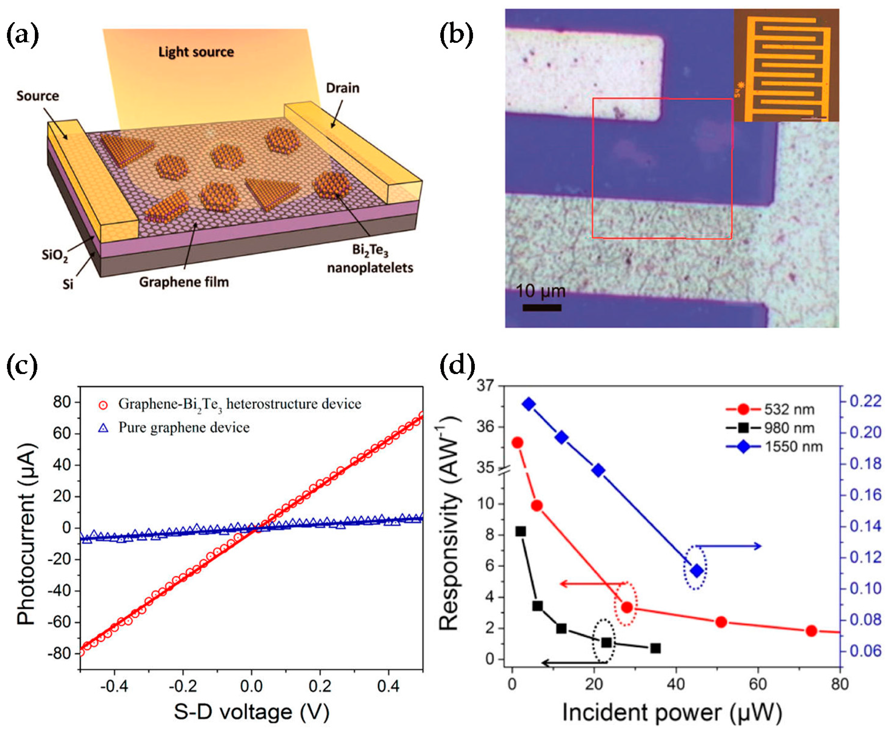
Another class of 2D materials, topological insulators, mainly Bi2Te3, Bi2Se3, Sb2Te3, are utilized to fabricate heterostructure materials with graphene. For example, Hong Qiao et al. has presented an effective broadband (from vis to IR) photodetector based on a graphene-Bi2Te3 heterostructure [74]. Similar to graphene-based materials, the crystal structure of Bi2Te3 is comprised of typical layered materials via van der Waals interactions with a hexagonal unit cell. Hence, large area epitaxial growth of Bi2Te3 nanocrystals on graphene templates is feasible. The schematic and optical images of such heterostructure phototransistor devices are illustrated in Figure 3a,b. For comparison, photocurrent results of two different devices based on monolayer graphene and heterostructure materials without applying the gate bias are presented in Figure 3c. It is obvious that the photocurrent of the heterostructure device is about 10 times higher than that of the pure graphene device. From Figure 3d, different wavelengths show high photoresponsivity which proves such heterostructured devices are capable of broadband photodetection from visible to NIR regime. The highest photoresponsivity is shown at the visible region (532 nm) (about 35 A W−1 at an excitation power of 1.28 μW).
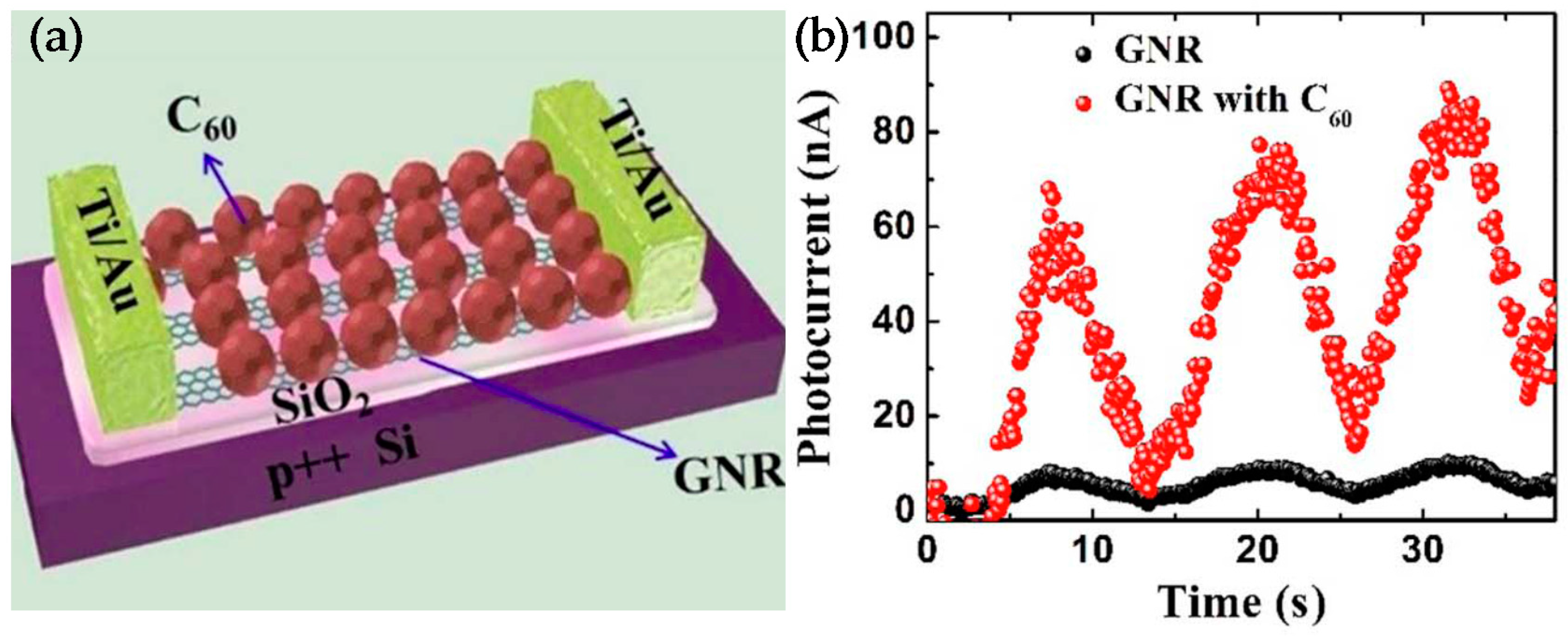
In these graphene-hybridized semiconductor systems, the light absorption mainly depends on the semiconductors, where graphene functions only as a carrier transporting layer. Hence, the broadband absorption characteristics of graphene have not been fully utilized in these heterojunctions. In order to overcome the disadvantages, graphene nanoribbons (GNRs) have been adopted to engineer the band structure of hybrid graphene photodetectors [78]. The absorption of GNR-based phototransistors is broadband and determined by the pertinent bandgap opening in the GNR, which can be controlled by the nanoribbon width. For example, a novel photodetector has been fabricated by Xuechao Yu et al. which is composed of GNRs with fullerene (C60) film (Figure 4a) [79]. The photoresponse of this GNR-C60 hybrid phototransistor under global irradiation is ∼0.4 A W−1, as shown in Figure 4b, which is about one order higher than the bare GNR phototransistor.
3.2. Hybrid Semiconductor Materials with p-n Junctions
Besides graphene-based heterojuctions, p-n junctions provide another platform to improve photoresponse [80]. As we know, p-n junctions are the basic building blocks of many optoelectronic devices, which have been utilized for rational control of their fundamental parameters, such as the bandgap, mobility and effective mass of charge carriers. Therefore, vertical p-n heterojunctions based on distinct layered materials have been widely used. For example, a heterojunction p-n diode based on phosphorene/monolayer MoS2 has been fabricated by van der Waals forces [81], which exhibits excellent current-rectifying characteristics and high Ilight/Idark ratio, up to 3 × 10³. In addition, graphene p-n junctions [82,83,84], TMD p-n junctions [85] and BP p-n junctions [86,87] have been constructed and exhibited high responsivity, due to effective separations of photo-generated electron/hole pairs by internal electric fields.
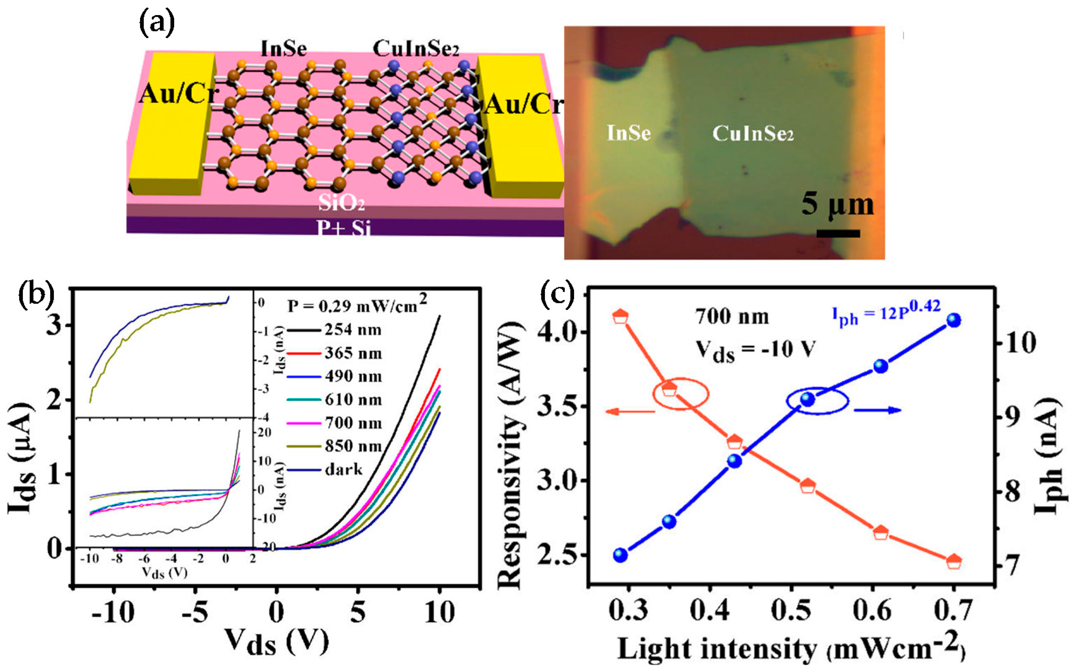
As shown in Figure 5a, Wei Feng et al. have fabricated a lateral thin-film InSe/CuInSe2 p-n hereojunction by a simple chemical doping procedure [88]. This lateral diode exhibits a broadband photoresponse ranging from 254 nm to 850 nm, because of the small band gaps of InSe and CuInSe2 (Figure 5b). Meanwhile, a large responsivity of 4.2 A W−1 is obtained at a wavelength of 700 nm with illumination power of 0.29 mW cm−2 and bias voltage of Vds = −10 V (Figure 5c). Such excellent performance of this p-n diode is attributed to bandgap engineering by selecting desired materials and high optical absorption by increasing channel thickness.
4. Device Structure Engineering for High Performance 2D Photodetectors
In addition to tailoring the material compositions, device structure engineering is an alternative route to improve sensitivity and response speed. Typical 2D layered semiconductors usually have their own distinct band gaps. The contact resistance at the electrode/semiconductor interface is often a dominating factor in the case of optoelectronic devices [89,90,91]. Meanwhile, the local electric field enhancements in devices can improve photoresponse. Hence, various device architectures were rationally designed to reduce the contact resistance or increase the local field of material systems (such as forming plasmonic Schottky contact), which are reviewed in detail in this section.
4.1. Graphene (Gr)-Semiconductor-Gr-Structured Devices
Contact resistance between semiconducting channels and electrodes plays an important role in device performance [92]. The common device structure for photodetector fabrication is metal–semiconductor–metal-based. One challenge in this field for high-quality photodetectors is optimizing metal contacts without damage or introduction of Fermi level at the interface of metal and semiconductor. To date, substantial research has been carried out on investigating the contact properties between semiconductor materials and different metal electrodes [93].
Besides different metal electrodes, graphene (Gr) as a promising electrode has been utilized to construct high performance 2D photoresponse devices. Unlike bulk metals, graphene is chemically inert and thus acts as an ideal contact in absence of diffusion and reaction with semiconductor crystals. Because of the finite density states of graphene, the graphene’s Fermi level can be tuned to obtain low contact resistance [94,95] or even a barrier-free contact with a semiconductor [96].
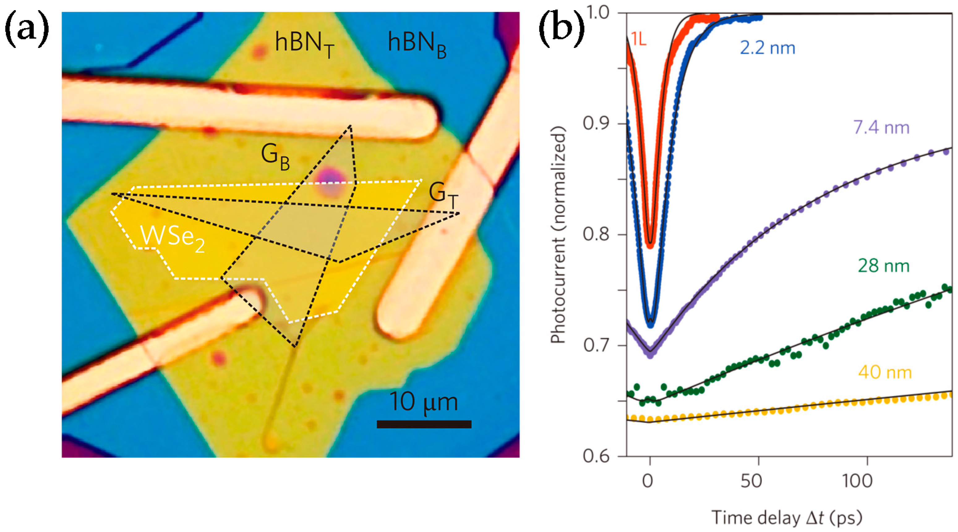
Haijie Tan et al., for example, fabricated Gr-WS2-Gr photodetectors through a simple chemical vapor deposition (CVD) grown process (Figure 6a) [97]. In this device, graphene layers are employed as work-function tunable electrodes, while WS2 is utilized as a photoactive material, which displays strong light–matter interaction and photon absorption. The greatest photoresponsivity of this Gr-WS2-Gr photodetector is 3.5 A W−1 under illumination power densities of 2.5 × 10⁷ mW cm−2 (Figure 6b). Figure 6c shows the time-resolved photoresponse with 200-nm channel length and a corresponding on/off ratio of 54. Similarly, M. Massicotte et al. constructed a high-quality photodetector based on G/WSe2/G van der Waals heterostructures [71]. Figure 7a shows the schematic image of the heterostructure. The value of photoresponse time was calculated from time-resolved photocurrent measurements on with different layer thicknesses (Figure 7b). The shortest photoresponse time is 5.5 ps. Incorporating graphene electrodes in other semiconductors is an efficient approach for high performing ultrathin photodetectors and would provide insights on the contact engineering in 2D optoelectronics.
4.2. Top-Gated Architecture Devices
In general, researchers always apply additional gate bias (Vg) and large drain-source bias (Vsd) for obtaining high photosensitivity. Some traditional dielectric materials (SiO [9], HfO2 [31] and Al2O3 [10]) are usually selected as gate dielectrics in the photoresponse devices. Despite the rapid progress that has been made on those dielectric materials, there is keen interest in the science community to utilize new dielectrics for exploring new physics and functionalities [98,99,100,101,102]. For example, using polymer electrolytes as the gate material is an efficient strategy to tune the carrier density and improve the photoresponse of the device [103]. Among promising candidates, ferroelectric is another unique option because of the ultrahigh dielectric constants and nonlinear, hysteretic dielectric response to an electric field [104]. Recently, poly(vinylidene fluoride-trifluoroethylene) (P (VDF-TrFE)) ferroelectric polymer films have been used as the new gate dielectric materials [105] and coated on the top of the semiconductors (MoS2) [106]. As shown in Figure 8a,b, Xudong Wang et al. fabricated a ferroelectric polarization gating MoS2 photodetector. The ferroelectric film can help to tune the transport properties of the channel, because its stable remnant polarization enables to offer an ultrahigh local electrostatic field (≈109 V m−1 within a several nanometer scale) in the semiconductor channel. Compared with the traditional MoS2 field effect transistor (FET) photodetectors, this device shows outstanding photodetection capabilities. Figure 8c illustrates that the device exhibits a maximum attainable photoresponsivity and high detectivity of 2.2 × 10¹² Jones. Furthermore, the stability of the photodetectors is also excellent and the signals remain nearly unchanged after 90,000 cycles of operation (as shown in Figure 8d). Hence, developing the device structure by utilization of the improved gate dielectric materials is an attractive research field for next-generation high performance 2D electronic/optoelectronic devices.
4.3. Designed Plasmonic Nanostructures in Devices
Enhancing the local field on thin layers is an efficient strategy to boost the currently limited absorption of 2D material and provide wavelength selectivity. Plasmonics as a kind of hybrid electromagnetic wave can rise from collective oscillations of the free electron gas within the metal surfaces [107,108]. Hence, the formation of plasmonics would help in increasing the local field to increase the photosensitivity [109]. Thanks to the tremendous progress in nanotechnologies, various metallic structures have been rationally designed and fabricated in recent years [110].
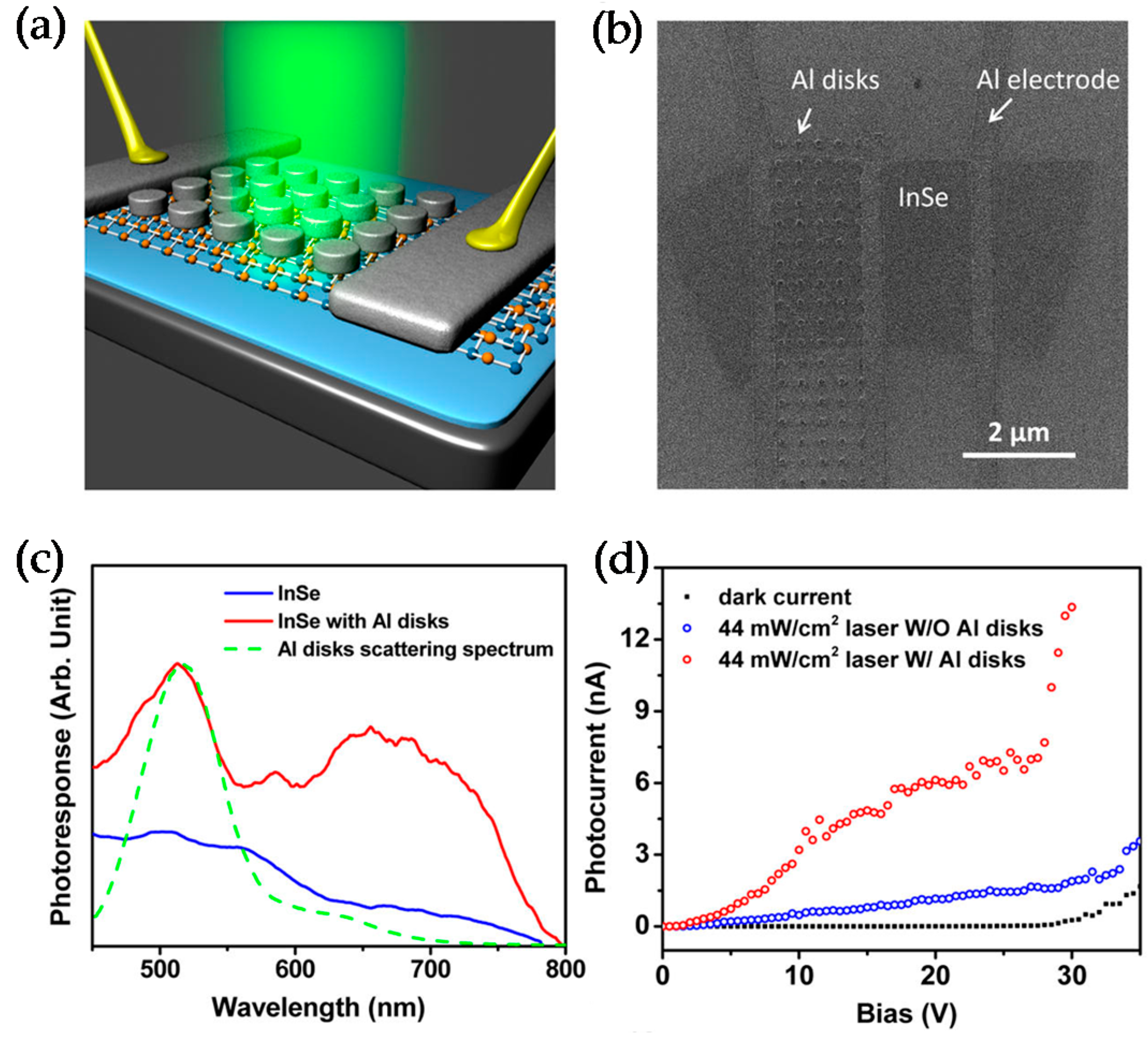
Sidong Lei et al. has achieved plasmonic enhancements for the photosensitivity by patterning arrays of Al nanodisks onto an InSe layer [111]. As shown in Figure 9a,b, plasmonic Al disk nanoantennas were fabricated onto the device. With the help of patterned Al disks, the absorption of the device is enhanced and the device photoresponse is also obviously enhanced in the 650– 750 nm range shown in Figure 9c, which is attributed to electron emission from the Fermi level of Al nanodisks into InSe. Meanwhile, the presence of Al nanodisks brings plasmonic enhancement collectively and therefore helps to improve the external quantum efficiency (Figure 9d).
5. Conclusions
This review provides an overview of recent advances in the rapidly developing field of 2D photodetectors. Continuous progress in this field has been witnessed by precisely controlling the components of the desired 2D materials, as well as rational engineering of device architectures. We first introduced the 2D photodetectors based on single-component materials and their inherent properties (such as operating wavelength, crystals and photoresponsivity). Then, we tried to summarize the accepted methods in rational tailoring 2D material systems for improved photoresponse. After that, device architecture engineering was demonstrated to provide another platform for high sensitivity and response of the photodetectors.
Although many breakthroughs have been achieved, some limitations are still present in the field of 2D photodetectors. Here, we list a few examples. First, the responses of some 2D devices are not fast enough for the real detector functions. Second, low-frequency (1/f) noise should be achieved and investigated for various 2D photodetectors, because it is considered as an important metric for evaluating the performance and benchmarking of such devices [112,113]. Third, sometimes current saturation occurs fast in some 2D materials, which will influence the photoconductivity and therefore detector performance.
Hence, there is a long way to go for the study of this field. First, a deeper understanding is required of the synergistic effects among each component, which will provide the direction for the heterojunction material design. Before that, more efforts should be directed to the fabrication and modification of 2D semiconductors with more excellent optoelectronic properties. Meanwhile, increasing fundamental research shall be carried out to investigate the structure-property relationships in 2D semiconductor systems. Furthermore, an effective large scale and hierarchical assembly process should be developed to meet the requirements of device architecture engineering for functional applications.
Of course, those challenges faced by the researchers will bring many opportunities as well; and some new characterizations are important [114,115,116]. After solving the riddles, more advances can be explored in the 2D material systems and device fabrication technologies, which will lead to exciting discoveries and opportunities in the further development of 2D photodetectors. For example, first, novel concepts in the materials epitaxy are attractive for constructing 2D heterojunctions and avoiding contaminations to the interfaces, bringing improved optoelectronic properties. Second, plasmonic nanostructures in the device fabrications remain largely unexplored, which could enhance the absorption of 2D materials and provide wavelength selectivity. It looks promising that many achievements in 2D photodetectors will be further attained to meet the demands of various applications.
Acknowledgments
This work was financially supported by the Fund of Ministry of Education of China (No. 2015RC034), China Postdoctoral Science Foundation (Nos. 2015M570924 and 2016T90030), the National Natural Science Foundation of China (No. 51603010). The authors appreciate the support from the “1000 Youth Talent plan” project and the “Excellent One Hundred” project of Beijing JiaoTong University.
Author Contributions
Qiuhong Cui, Yijun Yang and Junmeng Li wrote the paper, Feng Teng and Xi Wang designed the architecture and supervised the process of the paper.
Conflicts of Interest
The authors declare no conflict of interest.
References
- Tian, W.; Zhi, C.; Zhai, T.; Chen, S.; Wang, X.; Liao, M.; Golberg, D.; Bando, Y. In-doped Ga2O3 nanobelt based photodetector with high sensitivity and wide-range photoresponse. J. Mater. Chem. 2012, 22, 17984–17991. [Google Scholar] [CrossRef]
- Wang, X.; Tian, W.; Liao, M.; Bando, Y.; Golberg, D. Recent advances in solution-processed inorganic nanofilm photodetectors. Chem. Soc. Rev. 2014, 43, 1400–1422. [Google Scholar] [CrossRef] [PubMed]
- Mudd, G.W.; Svatek, S.A.; Ren, T.; Patanè, A.; Makarovsky, O.; Eaves, L.; Beton, P.H.; Kovalyuk, Z.D.; Lashkarev, G.V.; Kudrynskyi, Z.R.; et al. Tuning the bandgap of exfoliated inse nanosheets by quantum confinement. Adv. Mater. 2013, 25, 5714–5718. [Google Scholar] [CrossRef] [PubMed]
- Jacobs-Gedrim, R.B.; Shanmugam, M.; Jain, N.; Durcan, C.A.; Murphy, M.T.; Murray, T.M.; Matyi, R.J.; Moore, R.L.; Yu, B. Extraordinary photoresponse in two-dimensional In2Se3 nanosheets. ACS Nano 2014, 8, 514–521. [Google Scholar] [CrossRef] [PubMed]
- Chen, H.; Liu, H.; Zhang, Z.; Hu, K.; Fang, X. Nanostructured photodetectors: From ultraviolet to terahertz. Adv. Mater. 2016, 28, 403–433. [Google Scholar] [CrossRef] [PubMed]
- Huo, N.; Yang, S.; Wei, Z.; Li, S.-S.; Xia, J.-B.; Li, J. Photoresponsive and gas sensing field-effect transistors based on multilayer WS2 nanoflakes. Sci. Rep. 2014, 4, 5209. [Google Scholar] [CrossRef] [PubMed]
- Perea-López, N.; Elías, A.L.; Berkdemir, A.; Castro-Beltran, A.; Gutiérrez, H.R.; Feng, S.; Lv, R.; Hayashi, T.; López-Urías, F.; Ghosh, S.; et al. Photosensor device based on few-layered WS2 films. Adv. Funct. Mater. 2013, 23, 5511–5517. [Google Scholar] [CrossRef]
- Koppens, F.H.L.; Mueller, T.; Avouris, P.; Ferrari, A.C.; Vitiello, M.S.; Polini, M. Photodetectors based on graphene, other two-dimensional materials and hybrid systems. Nat. Nanotechnol. 2014, 9, 780–793. [Google Scholar] [CrossRef] [PubMed]
- Lopez-Sanchez, O.; Lembke, D.; Kayci, M.; Radenovic, A.; Kis, A. Ultrasensitive photodetectors based on monolayer MoS2. Nat. Nanotechnol. 2013, 8, 497–501. [Google Scholar] [CrossRef] [PubMed]
- Choi, W.; Cho, M.Y.; Konar, A.; Lee, J.H.; Cha, G.-B.; Hong, S.C.; Kim, S.; Kim, J.; Jena, D.; Joo, J.; et al. High-detectivity multilayer MoS2 phototransistors with spectral response from ultraviolet to infrared. Adv. Mater. 2012, 24, 5832–5836. [Google Scholar] [CrossRef] [PubMed]
- Zhou, Y.; Nie, Y.; Liu, Y.; Yan, K.; Hong, J.; Jin, C.; Zhou, Y.; Yin, J.; Liu, Z.; Peng, H. Epitaxy and photoresponse of two-dimensional gase crystals on flexible transparent mica sheets. ACS Nano 2014, 8, 1485–1490. [Google Scholar] [CrossRef] [PubMed]
- Zhang, W.; Chuu, C.-P.; Huang, J.-K.; Chen, C.-H.; Tsai, M.-L.; Chang, Y.-H.; Liang, C.-T.; Chen, Y.-Z.; Chueh, Y.-L.; He, J.-H.; et al. Ultrahigh-gain photodetectors based on atomically thin graphene-MoS2 heterostructures. Sci. Rep. 2014, 4, 3826. [Google Scholar] [CrossRef] [PubMed]
- Jariwala, D.; Marks, T.J.; Hersam, M.C. Mixed-dimensional van der waals heterostructures. Nat. Mater. 2017, 16, 170–181. [Google Scholar] [CrossRef] [PubMed]
- Chen, S.; Teng, C.; Zhang, M.; Li, Y.; Xie, D.; Shi, G. A flexible UV-VIS-NIR photodetector based on a perovskite/conjugated-polymer composite. Adv. Mater. 2016, 28, 5969–5974. [Google Scholar] [CrossRef] [PubMed]
- Jo, S.-H.; Kang, D.-H.; Shim, J.; Jeon, J.; Jeon, M.H.; Yoo, G.; Kim, J.; Lee, J.; Yeom, G.Y.; Lee, S.; et al. A high-performance WSe2/h-bn photodetector using a triphenylphosphine (PPh3)-based n-doping technique. Adv. Mater. 2016, 28, 4824–4831. [Google Scholar] [CrossRef] [PubMed]
- Huang, C.; Wu, S.; Sanchez, A.M.; Peters, J.J.P.; Beanland, R.; Ross, J.S.; Rivera, P.; Yao, W.; Cobden, D.H.; Xu, X. Lateral heterojunctions within monolayer MoSe2–WSe2 semiconductors. Nat. Mater. 2014, 13, 1096–1101. [Google Scholar] [CrossRef] [PubMed]
- Chang, Y.-H.; Zhang, W.; Zhu, Y.; Han, Y.; Pu, J.; Chang, J.-K.; Hsu, W.-T.; Huang, J.-K.; Hsu, C.-L.; Chiu, M.-H.; et al. Monolayer MoSe2 grown by chemical vapor deposition for fast photodetection. ACS Nano 2014, 8, 8582–8590. [Google Scholar] [CrossRef] [PubMed]
- Yang, S.; Li, Y.; Wang, X.; Huo, N.; Xia, J.-B.; Li, S.-S.; Li, J. High performance few-layer gas photodetector and its unique photo-response in different gas environments. Nanoscale 2014, 6, 2582–2587. [Google Scholar] [CrossRef] [PubMed]
- Hu, P.; Wang, L.; Yoon, M.; Zhang, J.; Feng, W.; Wang, X.; Wen, Z.; Idrobo, J.C.; Miyamoto, Y.; Geohegan, D.B.; et al. Highly responsive ultrathin gas nanosheet photodetectors on rigid and flexible substrates. Nano Lett. 2013, 13, 1649–1654. [Google Scholar] [CrossRef] [PubMed]
- Huang, Y.; Deng, H.-X.; Xu, K.; Wang, Z.-X.; Wang, Q.-S.; Wang, F.-M.; Wang, F.; Zhan, X.-Y.; Li, S.-S.; Luo, J.-W.; et al. Highly sensitive and fast phototransistor based on large size CVD-grown SnS2 nanosheets. Nanoscale 2015, 7, 14093–14099. [Google Scholar] [CrossRef] [PubMed]
- Song, J.; Xu, L.; Li, J.; Xue, J.; Dong, Y.; Li, X.; Zeng, H. Monolayer and few-layer all-inorganic perovskites as a new family of two-dimensional semiconductors for printable optoelectronic devices. Adv. Mater. 2016, 28, 4861–4869. [Google Scholar] [CrossRef] [PubMed]
- Li, X.; Yu, D.; Cao, F.; Gu, Y.; Wei, Y.; Wu, Y.; Song, J.; Zeng, H. Healing all-inorganic perovskite films via recyclable dissolution–recyrstallization for compact and smooth carrier channels of optoelectronic devices with high stability. Adv. Funct. Mater. 2016, 26, 5903–5912. [Google Scholar] [CrossRef]
- Dong, J.; Xue, Y.; Zhang, C.; Weng, Q.; Dai, P.; Yang, Y.; Zhou, M.; Li, C.; Cui, Q.; Kang, X.; et al. Improved Li+ storage through homogeneous n-doping within highly branched tubular graphitic foam. Adv. Mater. 2017, 29, 1603692. [Google Scholar] [CrossRef] [PubMed]
- Yang, Y.; Tang, D.-M.; Zhang, C.; Zhang, Y.; Liang, Q.; Chen, S.; Weng, Q.; Zhou, M.; Xue, Y.; Liu, J.; et al. “Protrusions” or “holes” in graphene: Which is the better choice for sodium ion storage? Energy & Environ. Sci. 2017. [Google Scholar] [CrossRef]
- Zhang, C.; Wang, X.; Liang, Q.; Liu, X.; Weng, Q.; Liu, J.; Yang, Y.; Dai, Z.; Ding, K.; Bando, Y.; et al. Amorphous phosphorus/nitrogen-doped graphene paper for ultrastable sodium-ion batteries. Nano Lett. 2016, 16, 2054–2060. [Google Scholar] [CrossRef] [PubMed]
- Liu, C.-H.; Chang, Y.-C.; Norris, T.B.; Zhong, Z. Graphene photodetectors with ultra-broadband and high responsivity at room temperature. Nat. Nanotechnol. 2014, 9, 273–278. [Google Scholar] [CrossRef] [PubMed]
- Mak, K.F.; Ju, L.; Wang, F.; Heinz, T.F. Optical spectroscopy of graphene: From the far infrared to the ultraviolet. Solid State Commun. 2012, 152, 1341–1349. [Google Scholar] [CrossRef]
- Xia, F.; Mueller, T.; Lin, Y.-m.; Valdes-Garcia, A.; Avouris, P. Ultrafast graphene photodetector. Nat. Nanotechnol. 2009, 4, 839–843. [Google Scholar] [CrossRef] [PubMed]
- Grigorenko, A.N.; Polini, M.; Novoselov, K.S. Graphene plasmonics. Nat. Photon. 2012, 6, 749–758. [Google Scholar] [CrossRef]
- Xia, F.; Wang, H.; Xiao, D.; Dubey, M.; Ramasubramaniam, A. Two-dimensional material nanophotonics. Nat. Photon. 2014, 8, 899–907. [Google Scholar] [CrossRef]
- Radisavljevic, B.; Radenovic, A.; Brivio, J.; Giacometti, V.; Kis, A. Single-layer MoS2 transistors. Nat. Nanotechnol. 2011, 6, 147–150. [Google Scholar] [CrossRef]
- Mak, K.F.; Shan, J. Photonics and optoelectronics of 2D semiconductor transition metal dichalcogenides. Nat. Photon. 2016, 10, 216–226. [Google Scholar] [CrossRef]
- Buscema, M.; Island, J.O.; Groenendijk, D.J.; Blanter, S.I.; Steele, G.A.; van der Zant, H.S.J.; Castellanos-Gomez, A. Photocurrent generation with two-dimensional van der waals semiconductors. Chem. Soc. Rev. 2015, 44, 3691–3718. [Google Scholar] [CrossRef] [PubMed]
- Wenjing, Z.; Qixing, W.; Yu, C.; Zhuo, W.; Andrew, T.S.W. Van der waals stacked 2D layered materials for optoelectronics. 2D Mater. 2016, 3, 022001. [Google Scholar] [CrossRef]
- Liu, F.; Shimotani, H.; Shang, H.; Kanagasekaran, T.; Zólyomi, V.; Drummond, N.; Fal’ko, V.I.; Tanigaki, K. High-sensitivity photodetectors based on multilayer gate flakes. ACS Nano 2014, 8, 752–760. [Google Scholar] [CrossRef] [PubMed]
- Coleman, J.N.; Lotya, M.; O’Neill, A.; Bergin, S.D.; King, P.J.; Khan, U.; Young, K.; Gaucher, A.; De, S.; Smith, R.J.; et al. Two-dimensional nanosheets produced by liquid exfoliation of layered materials. Science 2011, 331, 568–571. [Google Scholar] [CrossRef] [PubMed]
- Hasan, M.Z.; Kane, C.L. Colloquium: topological insulators. Rev. Mod. Phys. 2010, 82, 3045–3067. [Google Scholar] [CrossRef]
- Tian, W.; Zhang, C.; Zhai, T.; Li, S.-L.; Wang, X.; Liao, M.; Tsukagoshi, K.; Golberg, D.; Bando, Y. Flexible SnO2 hollow nanosphere film based high-performance ultraviolet photodetector. Chem. Commun. 2013, 49, 3739–3741. [Google Scholar] [CrossRef] [PubMed]
- Yu, P.; Yu, X.; Lu, W.; Lin, H.; Sun, L.; Du, K.; Liu, F.; Fu, W.; Zeng, Q.; Shen, Z.; et al. Fast photoresponse from 1t tin diselenide atomic layers. Adv. Funct. Mater. 2016, 26, 137–145. [Google Scholar] [CrossRef]
- Zhang, E.; Jin, Y.; Yuan, X.; Wang, W.; Zhang, C.; Tang, L.; Liu, S.; Zhou, P.; Hu, W.; Xiu, F. ReS2-based field-effect transistors and photodetectors. Adv. Funct. Mater. 2015, 25, 4076–4082. [Google Scholar] [CrossRef]
- Wu, J.; Koon, G.K.W.; Xiang, D.; Han, C.; Toh, C.T.; Kulkarni, E.S.; Verzhbitskiy, I.; Carvalho, A.; Rodin, A.S.; Koenig, S.P.; et al. Colossal ultraviolet photoresponsivity of few-layer black phosphorus. ACS Nano 2015, 9, 8070–8077. [Google Scholar] [CrossRef] [PubMed]
- Buscema, M.; Groenendijk, D.J.; Blanter, S.I.; Steele, G.A.; van der Zant, H.S.J.; Castellanos-Gomez, A. Fast and broadband photoresponse of few-layer black phosphorus field-effect transistors. Nano Lett. 2014, 14, 3347–3352. [Google Scholar] [CrossRef] [PubMed]
- Engel, M.; Steiner, M.; Avouris, P. Black phosphorus photodetector for multispectral, high-resolution imaging. Nano Lett. 2014, 14, 6414–6417. [Google Scholar] [CrossRef] [PubMed]
- Low, T.; Engel, M.; Steiner, M.; Avouris, P. Origin of photoresponse in black phosphorus phototransistors. Phys. Rev. B 2014, 90, 081408. [Google Scholar] [CrossRef]
- Ling, X.; Wang, H.; Huang, S.; Xia, F.; Dresselhaus, M.S. The renaissance of black phosphorus. Proc. Natl. Acad. Sci. USA 2015, 112, 4523–4530. [Google Scholar] [CrossRef] [PubMed]
- Zhao, Y.; Zhu, K. Organic-inorganic hybrid lead halide perovskites for optoelectronic and electronic applications. Chem. Soc. Rev. 2016, 45, 655–689. [Google Scholar] [CrossRef] [PubMed]
- Sichert, J.A.; Tong, Y.; Mutz, N.; Vollmer, M.; Fischer, S.; Milowska, K.Z.; García Cortadella, R.; Nickel, B.; Cardenas-Daw, C.; Stolarczyk, J.K.; et al. Quantum size effect in organometal halide perovskite nanoplatelets. Nano Lett. 2015, 15, 6521–6527. [Google Scholar] [CrossRef] [PubMed]
- Dou, L.; Wong, A.B.; Yu, Y.; Lai, M.; Kornienko, N.; Eaton, S.W.; Fu, A.; Bischak, C.G.; Ma, J.; Ding, T.; et al. Atomically thin two-dimensional organic-inorganic hybrid perovskites. Science 2015, 349, 1518–1521. [Google Scholar] [CrossRef] [PubMed]
- Wehrenfennig, C.; Eperon, G.E.; Johnston, M.B.; Snaith, H.J.; Herz, L.M. High charge carrier mobilities and lifetimes in organolead trihalide perovskites. Adv. Mater. 2014, 26, 1584–1589. [Google Scholar] [CrossRef] [PubMed]
- Wang, Q.H.; Kalantar-Zadeh, K.; Kis, A.; Coleman, J.N.; Strano, M.S. Electronics and optoelectronics of two-dimensional transition metal dichalcogenides. Nat. Nanotechnol. 2012, 7, 699–712. [Google Scholar] [CrossRef] [PubMed]
- Mak, K.F.; Lee, C.; Hone, J.; Shan, J.; Heinz, T.F. Atomically thin MoS2: A new direct-gap semiconductor. Phys. Rev. Lett. 2010, 105, 136805. [Google Scholar] [CrossRef] [PubMed]
- Kuc, A.; Zibouche, N.; Heine, T. Influence of quantum confinement on the electronic structure of the transition metal sulfide TS2. Phys. Rev. B 2011, 83, 245213. [Google Scholar] [CrossRef]
- Néstor, P.-L.; Zhong, L.; Nihar, R.P.; Agustín, I.-R.; Ana Laura, E.; Amber, M.; Jun, L.; Pulickel, M.A.; Humberto, T.; Luis, B.; et al. Cvd-grown monolayered mos 2 as an effective photosensor operating at low-voltage. 2D Mater. 2014, 1, 011004. [Google Scholar] [CrossRef]
- Fivaz, R.; Mooser, E. Mobility of charge carriers in semiconducting layer structures. Phys. Rev. 1967, 163, 743–755. [Google Scholar] [CrossRef]
- Pradhan, N.R.; Ludwig, J.; Lu, Z.; Rhodes, D.; Bishop, M.M.; Thirunavukkuarasu, K.; McGill, S.A.; Smirnov, D.; Balicas, L. High photoresponsivity and short photoresponse times in few-layered WSe2 transistors. ACS Appl. Mater. & Interfaces 2015, 7, 12080–12088. [Google Scholar] [CrossRef]
- Island, J.O.; Buscema, M.; Barawi, M.; Clamagirand, J.M.; Ares, J.R.; Sánchez, C.; Ferrer, I.J.; Steele, G.A.; van der Zant, H.S.J.; Castellanos-Gomez, A. Ultrahigh photoresponse of few-layer TiS3 nanoribbon transistors. Adv. Opt. Mater. 2014, 2, 641–645. [Google Scholar] [CrossRef]
- Jian, H.; Wenhui, W.; Qi, F.; Lei, Y.; Kun, Z.; Jingyu, Z.; Bin, X. Stable electrical performance observed in large-scale monolayer WSe2(1−x)S2x with tunable band gap. Nanotechnology 2016, 27, 13LT01. [Google Scholar] [CrossRef]
- Feng, Q.; Zhu, Y.; Hong, J.; Zhang, M.; Duan, W.; Mao, N.; Wu, J.; Xu, H.; Dong, F.; Lin, F.; et al. Growth of large-area 2D MoS2(1−x)Se2x semiconductor alloys. Adv. Mater. 2014, 26, 2648–2653. [Google Scholar] [CrossRef] [PubMed]
- Late, D.J.; Liu, B.; Luo, J.; Yan, A.; Matte, H.S.S.R.; Grayson, M.; Rao, C.N.R.; Dravid, V.P. Gas and gase ultrathin layer transistors. Adv. Mater. 2012, 24, 3549–3554. [Google Scholar] [CrossRef] [PubMed]
- Tamalampudi, S.R.; Lu, Y.-Y.; Kumar U, R.; Sankar, R.; Liao, C.-D.; Moorthy B, K.; Cheng, C.-H.; Chou, F.C.; Chen, Y.-T. High performance and bendable few-layered inse photodetectors with broad spectral response. Nano Lett. 2014, 14, 2800–2806. [Google Scholar] [CrossRef] [PubMed]
- Zhou, X.; Gan, L.; Tian, W.; Zhang, Q.; Jin, S.; Li, H.; Bando, Y.; Golberg, D.; Zhai, T. Photodetectors: Ultrathin SnSe2 flakes grown by chemical vapor deposition for high-performance photodetectors. Adv. Mater. 2015, 27, 8119. [Google Scholar] [CrossRef]
- Song, H.S.; Li, S.L.; Gao, L.; Xu, Y.; Ueno, K.; Tang, J.; Cheng, Y.B.; Tsukagoshi, K. High-performance top-gated monolayer SnS2 field-effect transistors and their integrated logic circuits. Nanoscale 2013, 5, 9666–9670. [Google Scholar] [CrossRef] [PubMed]
- Mun, H.; Yang, H.; Park, J.; Ju, C.; Char, K. High electron mobility in epitaxial SnO2-x in semiconducting regime. APL Mater. 2015, 3, 076107. [Google Scholar] [CrossRef]
- Qiao, J.; Kong, X.; Hu, Z.-X.; Yang, F.; Ji, W. High-mobility transport anisotropy and linear dichroism in few-layer black phosphorus. Nat. Commun. 2014, 5, 4475. [Google Scholar] [CrossRef] [PubMed]
- Leijtens, T.; Stranks, S.D.; Eperon, G.E.; Lindblad, R.; Johansson, E.M.J.; McPherson, I.J.; Rensmo, H.; Ball, J.M.; Lee, M.M.; Snaith, H.J. Electronic properties of meso-superstructured and planar organometal halide perovskite films: Charge trapping, photodoping, and carrier mobility. ACS Nano 2014, 8, 7147–7155. [Google Scholar] [CrossRef] [PubMed]
- Hong, X.; Kim, J.; Shi, S.-F.; Zhang, Y.; Jin, C.; Sun, Y.; Tongay, S.; Wu, J.; Zhang, Y.; Wang, F. Ultrafast charge transfer in atomically thin mos2/ws2 heterostructures. Nat. Nanotechnol. 2014, 9, 682–686. [Google Scholar] [CrossRef] [PubMed]
- Wang, X.; Weng, Q.; Yang, Y.; Bando, Y.; Golberg, D. Hybrid two-dimensional materials in rechargeable battery applications and their microscopic mechanisms. Chem. Soc. Rev. 2016, 45, 4042–4073. [Google Scholar] [CrossRef] [PubMed]
- Zhou, M.; Weng, Q.; Zhang, X.; Wang, X.; Xue, Y.; Zeng, X.; Bando, Y.; Golberg, D. In situ electrochemical formation of core-shell nickel-iron disulfide and oxyhydroxide heterostructured catalysts for a stable oxygen evolution reaction and the associated mechanisms. J. Mater. Chem. A 2017, 5, 4335–4342. [Google Scholar] [CrossRef]
- Weng, Q.; Wang, X.; Wang, X.; Bando, Y.; Golberg, D. Functionalized hexagonal boron nitride nanomaterials: Emerging properties and applications. Chem. Soc. Rev. 2016, 45, 3989–4012. [Google Scholar] [CrossRef] [PubMed]
- Roy, K.; Padmanabhan, M.; Goswami, S.; Sai, T.P.; Ramalingam, G.; Raghavan, S.; Ghosh, A. Graphene-MoS2 hybrid structures for multifunctional photoresponsive memory devices. Nat. Nanotechnol. 2013, 8, 826–830. [Google Scholar] [CrossRef] [PubMed]
- Massicotte, M.; Schmidt, P.; Vialla, F.; Schädler, K.G.; Reserbat Plantey, A.; Watanabe, K.; Taniguchi, T.; Tielrooij, K.J.; Koppens, F.H.L. Picosecond photoresponse in van der waals heterostructures. Nat. Nanotechnol. 2016, 11, 42–46. [Google Scholar] [CrossRef] [PubMed]
- Huang, Y.Q.; Zhu, R.J.; Kang, N.; Du, J.; Xu, H.Q. Photoelectrical response of hybrid graphene-pbs quantum dot devices. Appl. Phys. Lett. 2013, 103, 143119. [Google Scholar] [CrossRef]
- Cheng, S.-H.; Weng, T.-M.; Lu, M.-L.; Tan, W.-C.; Chen, J.-Y.; Chen, Y.-F. All carbon-based photodetectors: An eminent integration of graphite quantum dots and two dimensional graphene. Sci. Rep. 2013, 3, 2694. [Google Scholar] [CrossRef] [PubMed]
- Qiao, H.; Yuan, J.; Xu, Z.; Chen, C.; Lin, S.; Wang, Y.; Song, J.; Liu, Y.; Khan, Q.; Hoh, H.Y.; et al. Broadband photodetectors based on graphene-Bi2Te3 heterostructure. ACS Nano 2015, 9, 1886–1894. [Google Scholar] [CrossRef] [PubMed]
- Lin, M.-Y.; Chang, C.-E.; Wang, C.-H.; Su, C.-F.; Chen, C.; Lee, S.-C.; Lin, S.-Y. Toward epitaxially grown two-dimensional crystal hetero-structures: Single and double MoS2/graphene hetero-structures by chemical vapor depositions. Appl. Phys. Lett. 2014, 105, 073501. [Google Scholar] [CrossRef]
- Wu, C.R.; Liao, K.C.; Wu, C.H.; Lin, S.Y. Luminescence enhancement and enlarged dirac point shift of MoS2/graphene hetero-structure photodetectors with postgrowth annealing treatment. IEEE J. Sel. Top. Quant. Electron. 2017, 23, 101–105. [Google Scholar] [CrossRef]
- Konstantatos, G.; Badioli, M.; Gaudreau, L.; Osmond, J.; Bernechea, M.; de Arquer, F.P.G.; Gatti, F.; Koppens, F.H.L. Hybrid graphene-quantum dot phototransistors with ultrahigh gain. Nat. Nanotechnol. 2012, 7, 363–368. [Google Scholar] [CrossRef] [PubMed]
- Yu, X.; Dong, Z.; Liu, Y.; Liu, T.; Tao, J.; Zeng, Y.; Yang, J.K.W.; Wang, Q.J. A high performance, visible to mid-infrared photodetector based on graphene nanoribbons passivated with HfO2. Nanoscale 2016, 8, 327–332. [Google Scholar] [CrossRef] [PubMed]
- Yu, X.; Dong, Z.; Yang, J.K.W.; Wang, Q.J. Room-temperature mid-infrared photodetector in all-carbon graphene nanoribbon-C60 hybrid nanostructure. Optica 2016, 3, 979–984. [Google Scholar] [CrossRef]
- Feng, W.; Wu, J.-B.; Li, X.; Zheng, W.; Zhou, X.; Xiao, K.; Cao, W.; Yang, B.; Idrobo, J.-C.; Basile, L.; et al. Ultrahigh photo-responsivity and detectivity in multilayer InSe nanosheets phototransistors with broadband response. J. Mater. Chem. C 2015, 3, 7022–7028. [Google Scholar] [CrossRef]
- Deng, Y.; Luo, Z.; Conrad, N.J.; Liu, H.; Gong, Y.; Najmaei, S.; Ajayan, P.M.; Lou, J.; Xu, X.; Ye, P.D. Black phosphorus–monolayer MoS2 van der waals heterojunction p-n diode. ACS Nano 2014, 8, 8292–8299. [Google Scholar] [CrossRef] [PubMed]
- Yu, X.; Wang, Q.J. Photodetector Based on Lateral Graphene p-n Junction Created by Electron-Beam Irradiation; Optical Society of America: San Jose, CA, USA, 2015. [Google Scholar]
- Liu, N.; Tian, H.; Schwartz, G.; Tok, J.B.H.; Ren, T.-L.; Bao, Z. Large-area, transparent, and flexible infrared photodetector fabricated using p-n junctions formed by n-doping chemical vapor deposition grown graphene. Nano Lett. 2014, 14, 3702–3708. [Google Scholar] [CrossRef] [PubMed]
- Herring, P.K.; Hsu, A.L.; Gabor, N.M.; Shin, Y.C.; Kong, J.; Palacios, T.; Jarillo-Herrero, P. Photoresponse of an electrically tunable ambipolar graphene infrared thermocouple. Nano Lett. 2014, 14, 901–907. [Google Scholar] [CrossRef] [PubMed]
- Baugher, B.W.H.; Churchill, H.O.H.; Yang, Y.; Jarillo-Herrero, P. Optoelectronic devices based on electrically tunable p-n diodes in a monolayer dichalcogenide. Nat. Nanotechnol. 2014, 9, 262–267. [Google Scholar] [CrossRef] [PubMed]
- Yuan, H.; Liu, X.; Afshinmanesh, F.; Li, W.; Xu, G.; Sun, J.; Lian, B.; Curto, A.G.; Ye, G.; Hikita, Y.; et al. Polarization-sensitive broadband photodetector using a black phosphorus vertical p-n junction. Nat. Nanotechnol. 2015, 10, 707–713. [Google Scholar] [CrossRef] [PubMed]
- Yu, X.; Zhang, S.; Zeng, H.; Wang, Q.J. Lateral black phosphorene p-n junctions formed via chemical doping for high performance near-infrared photodetector. Nano Energy 2016, 25, 34–41. [Google Scholar] [CrossRef]
- Feng, W.; Zheng, W.; Chen, X.; Liu, G.; Cao, W.; Hu, P. Solid-state reaction synthesis of a InSe/CuInSe2 lateral p-n heterojunction and application in high performance optoelectronic devices. Chem. Mater. 2015, 27, 983–989. [Google Scholar] [CrossRef]
- Zhang, W.; Chiu, M.-H.; Chen, C.-H.; Chen, W.; Li, L.-J.; Wee, A.T.S. Role of metal contacts in high-performance phototransistors based on WSe2 monolayers. ACS Nano 2014, 8, 8653–8661. [Google Scholar] [CrossRef] [PubMed]
- Monroy, E.; Omnès, F.; Calle, F. Wide-bandgap semiconductor ultraviolet photodetectors. Semicond. Sci. Tech. 2003, 18, R33. [Google Scholar] [CrossRef]
- Fan, Y.; Zhou, Y.; Wang, X.; Tan, H.; Rong, Y.; Warner, J.H. Photoinduced schottky barrier lowering in 2D monolayer WS2 photodetectors. Adv. Opt. Mater. 2016, 4, 1573–1581. [Google Scholar] [CrossRef]
- Allain, A.; Kang, J.; Banerjee, K.; Kis, A. Electrical contacts to two-dimensional semiconductors. Nat. Mater. 2015, 14, 1195–1205. [Google Scholar] [CrossRef] [PubMed]
- Das, S.; Chen, H.-Y.; Penumatcha, A.V.; Appenzeller, J. High performance multilayer MoS2 transistors with scandium contacts. Nano Lett. 2013, 13, 100–105. [Google Scholar] [CrossRef] [PubMed]
- Shih, C.-J.; Wang, Q.H.; Son, Y.; Jin, Z.; Blankschtein, D.; Strano, M.S. Tuning on–off current ratio and field-effect mobility in a MoS2-graphene heterostructure via schottky barrier modulation. ACS Nano 2014, 8, 5790–5798. [Google Scholar] [CrossRef] [PubMed]
- Yu, L.; Lee, Y.-H.; Ling, X.; Santos, E.J.G.; Shin, Y.C.; Lin, Y.; Dubey, M.; Kaxiras, E.; Kong, J.; Wang, H.; et al. Graphene/MoS2 hybrid technology for large-scale two-dimensional electronics. Nano Lett. 2014, 14, 3055–3063. [Google Scholar] [CrossRef] [PubMed]
- Liu, Y.; Wu, H.; Cheng, H.-C.; Yang, S.; Zhu, E.; He, Q.; Ding, M.; Li, D.; Guo, J.; Weiss, N.O.; et al. Toward barrier free contact to molybdenum disulfide using graphene electrodes. Nano Lett. 2015, 15, 3030–3034. [Google Scholar] [CrossRef] [PubMed]
- Tan, H.; Fan, Y.; Zhou, Y.; Chen, Q.; Xu, W.; Warner, J.H. Ultrathin 2D photodetectors utilizing chemical vapor deposition grown WS2 with graphene electrodes. ACS Nano 2016, 10, 7866–7873. [Google Scholar] [CrossRef] [PubMed]
- Panzer, M.J.; Newman, C.R.; Frisbie, C.D. Low-voltage operation of a pentacene field-effect transistor with a polymer electrolyte gate dielectric. Appl. Phys. Lett. 2005, 86, 103503. [Google Scholar] [CrossRef]
- Panzer, M.J.; Frisbie, C.D. Polymer electrolyte gate dielectric reveals finite windows of high conductivity in organic thin film transistors at high charge carrier densities. J. Am. Chem. Soc. 2005, 127, 6960–6961. [Google Scholar] [CrossRef] [PubMed]
- Ohno, Y.; Maehashi, K.; Yamashiro, Y.; Matsumoto, K. Electrolyte-gated graphene field-effect transistors for detecting PH and protein adsorption. Nano Lett. 2009, 9, 3318–3322. [Google Scholar] [CrossRef] [PubMed]
- Panzer, M.J.; Frisbie, C.D. Exploiting ionic coupling in electronic devices: Electrolyte-gated organic field-effect transistors. Adv. Mater. 2008, 20, 3177–3180. [Google Scholar] [CrossRef]
- Kim, S.H.; Hong, K.; Xie, W.; Lee, K.H.; Zhang, S.; Lodge, T.P.; Frisbie, C.D. Electrolyte-gated transistors for organic and printed electronics. Adv. Mater. 2013, 25, 1822–1846. [Google Scholar] [CrossRef] [PubMed]
- Lhuillier, E.; Robin, A.; Ithurria, S.; Aubin, H.; Dubertret, B. Electrolyte-gated colloidal nanoplatelets-based phototransistor and its use for bicolor detection. Nano Lett. 2014, 14, 2715–2719. [Google Scholar] [CrossRef] [PubMed]
- Zheng, Y.; Ni, G.-X.; Toh, C.-T.; Tan, C.-Y.; Yao, K.; Özyilmaz, B. Graphene field-effect transistors with ferroelectric gating. Phys. Rev. Lett. 2010, 105, 166602. [Google Scholar] [CrossRef] [PubMed]
- Guangjian, W.; Xudong, W.; Peng, W.; Hai, H.; Yan, C.; Shuo, S.; Hong, S.; Tie, L.; Jianlu, W.; Shangtao, Z.; et al. Visible to short wavelength infrared In2Se3-nanoflake photodetector gated by a ferroelectric polymer. Nanotechnology 2016, 27, 364002. [Google Scholar] [CrossRef]
- Wang, X.; Wang, P.; Wang, J.; Hu, W.; Zhou, X.; Guo, N.; Huang, H.; Sun, S.; Shen, H.; Lin, T.; et al. Ultrasensitive and broadband MoS2 photodetector driven by ferroelectrics. Adv. Mater. 2015, 27, 6575–6581. [Google Scholar] [CrossRef] [PubMed]
- Schuller, J.A.; Barnard, E.S.; Cai, W.; Jun, Y.C.; White, J.S.; Brongersma, M.L. Plasmonics for extreme light concentration and manipulation. Nat. Mater. 2010, 9, 193–204. [Google Scholar] [CrossRef] [PubMed]
- Echtermeyer, T.J.; Britnell, L.; Jasnos, P.K.; Lombardo, A.; Gorbachev, R.V.; Grigorenko, A.N.; Geim, A.K.; Ferrari, A.C.; Novoselov, K.S. Strong plasmonic enhancement of photovoltage in graphene. Nat. Commun. 2011, 2, 458. [Google Scholar] [CrossRef] [PubMed]
- Goykhman, I.; Sassi, U.; Desiatov, B.; Mazurski, N.; Milana, S.; de Fazio, D.; Eiden, A.; Khurgin, J.; Shappir, J.; Levy, U.; et al. On-chip integrated, silicon-graphene plasmonic schottky photodetector with high responsivity and avalanche photogain. Nano Lett. 2016, 16, 3005–3013. [Google Scholar] [CrossRef] [PubMed]
- Atwater, H.A.; Polman, A. Plasmonics for improved photovoltaic devices. Nat. Mater. 2010, 9, 205–213. [Google Scholar] [CrossRef] [PubMed]
- Lei, S.; Wen, F.; Ge, L.; Najmaei, S.; George, A.; Gong, Y.; Gao, W.; Jin, Z.; Li, B.; Lou, J.; et al. An atomically layered InSe avalanche photodetector. Nano Lett. 2015, 15, 3048–3055. [Google Scholar] [CrossRef] [PubMed]
- Das, S.R.; Kwon, J.; Prakash, A.; Delker, C.J.; Das, S.; Janes, D.B. Low-frequency noise in MoSe2 field effect transistors. Appl. Phys. Lett. 2015, 106, 083507. [Google Scholar] [CrossRef]
- Liu, G.; Stillman, W.; Rumyantsev, S.; Shao, Q.; Shur, M.; Balandin, A.A. Low-frequency electronic noise in the double-gate single-layer graphene transistors. Appl. Phys. Lett. 2009, 95, 033103. [Google Scholar] [CrossRef]
- Hou, G.; Cheng, B.; Cao, Y.; Yao, M.; Li, B.; Zhang, C.; Weng, Q.; Wang, X.; Bando, Y.; Golberg, D.; et al. Scalable production of 3D plum-pudding-like Si/C spheres: Towards practical application in Li-ion batteries. Nano Energy 2016, 24, 111–120. [Google Scholar] [CrossRef]
- Wang, X.; Liu, D.; Weng, Q.; Liu, J.; Liang, Q.; Zhang, C. Cu/Li4Ti5O12 scaffolds as superior anodes for lithium-ion batteries. NPG Asia Mater. 2015, 7, e171. [Google Scholar] [CrossRef]
- Yang, Y.; Liu, X.; Dai, Z.; Yuan, F.; Bando, Y.; Golberg, D. In Situ Electrochemistry of Rechargeable Battery Materials: Status Report and Perspective. Adv. Mater. 2017. [Google Scholar] [CrossRef]
Figure 1.
(a) Schematic of the graphene-quantum dot hybrid phototransistor. (b) Spectral responsivity of the hybrid photodetector.
Figure 1.
(a) Schematic of the graphene-quantum dot hybrid phototransistor. (b) Spectral responsivity of the hybrid photodetector.
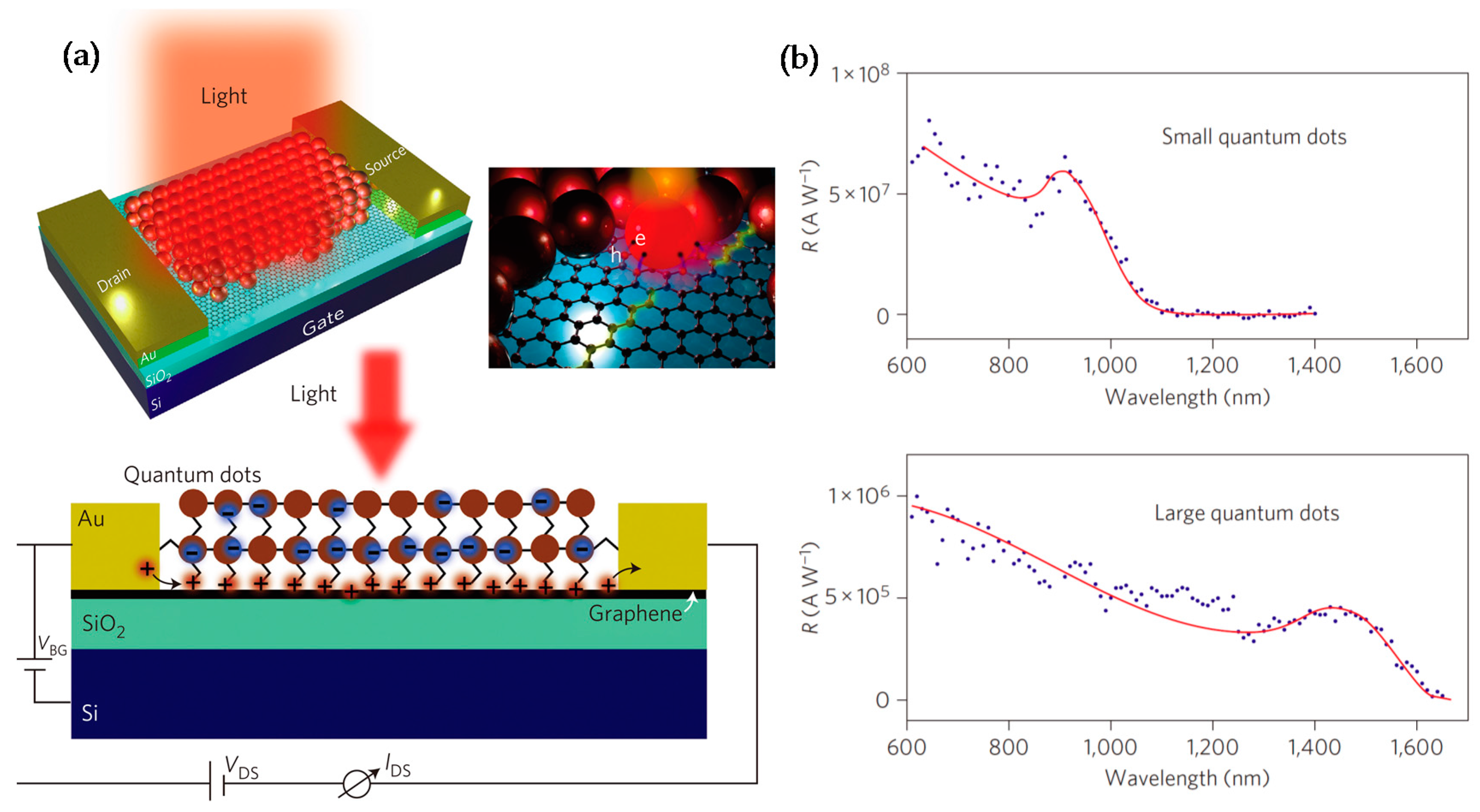
Figure 2.
(a) Schematics of graphene/MoS2 layered structure. (b) photoresponsivity of graphene/MoS2 photodetectors. (c) Light energy-dependent photoresponsivity.
Figure 2.
(a) Schematics of graphene/MoS2 layered structure. (b) photoresponsivity of graphene/MoS2 photodetectors. (c) Light energy-dependent photoresponsivity.

Figure 3.
Schematic (a) and optical (b) image of the heterostructure phototransistor device. (c) Photocurrent profile with respect to source-drain voltage. (d) Device photoresponsivity under different incident power at 532, 980, and 1550 nm, respectively.
Figure 3.
Schematic (a) and optical (b) image of the heterostructure phototransistor device. (c) Photocurrent profile with respect to source-drain voltage. (d) Device photoresponsivity under different incident power at 532, 980, and 1550 nm, respectively.

Figure 4.
(a) Schematic design of the hybrid graphene nanoribbon (GNR)-C60 nanostructure. (b) Time-resolved photocurrent of GNR-C60 hybrid phototransistor and bare GNR phototransistor.
Figure 4.
(a) Schematic design of the hybrid graphene nanoribbon (GNR)-C60 nanostructure. (b) Time-resolved photocurrent of GNR-C60 hybrid phototransistor and bare GNR phototransistor.

Figure 5.
(a) Schematic and optical image of a InSe/CuInSe2 p-n heterostructure. (b) Photocurrent of a p-n diode under various illumination wavelengths at 0.29 mW cm−2. (c) Photocurrent and responsivity as a function of optical intensity.
Figure 5.
(a) Schematic and optical image of a InSe/CuInSe2 p-n heterostructure. (b) Photocurrent of a p-n diode under various illumination wavelengths at 0.29 mW cm−2. (c) Photocurrent and responsivity as a function of optical intensity.

Figure 6.
(a) Schematic three-dimensional (3D) and optical images of a Gr-WS2-Gr photodetector. (b) Photoresponsivity of the four types of detectors. (c) The time-resolved photoresponse of the device.
Figure 6.
(a) Schematic three-dimensional (3D) and optical images of a Gr-WS2-Gr photodetector. (b) Photoresponsivity of the four types of detectors. (c) The time-resolved photoresponse of the device.

Figure 7.
(a) Optical image of a heterostructure. GT and GB are the top and bottom graphene layers, respectively. (b) Time-resolved photocurrent measurements with different layer thicknesses.
Figure 7.
(a) Optical image of a heterostructure. GT and GB are the top and bottom graphene layers, respectively. (b) Time-resolved photocurrent measurements with different layer thicknesses.

Figure 8.
Optical (a) and 3D schematic (b) view of the device. (c) Photoresponsivity and detectivity of the device under various incident power. (d) Photocurrent response during 90,000 cycles of operation.
Figure 8.
Optical (a) and 3D schematic (b) view of the device. (c) Photoresponsivity and detectivity of the device under various incident power. (d) Photocurrent response during 90,000 cycles of operation.
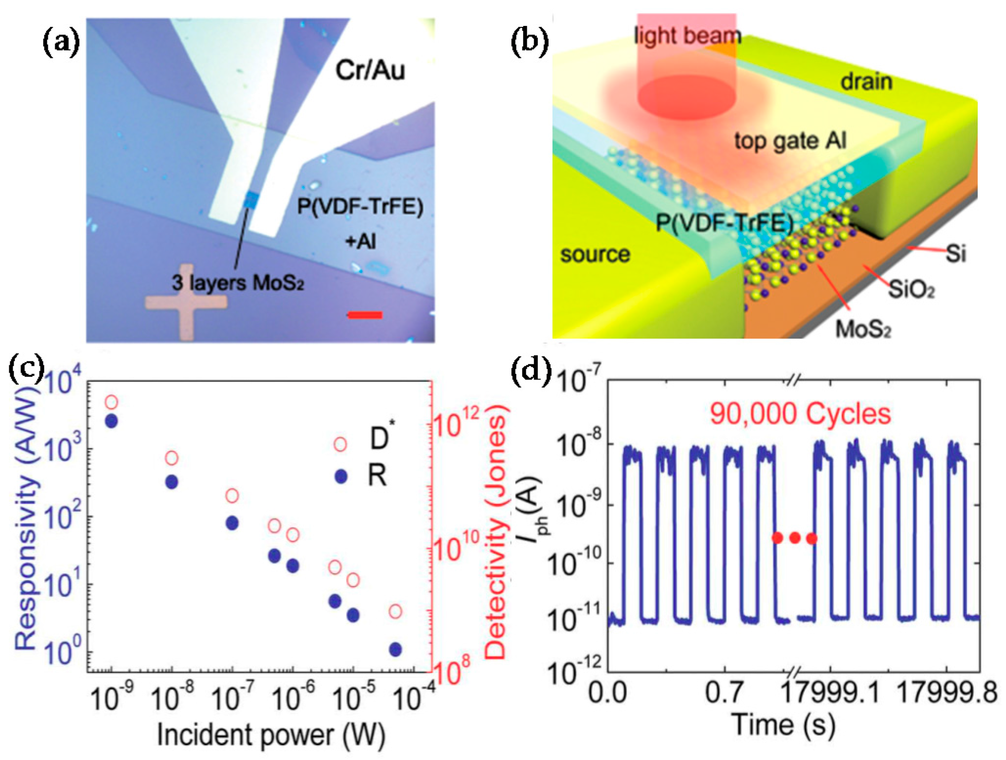
Figure 9.
Schematic (a) and SEM (b) image of an Al nanodisk plasmon-enhanced InSe avalanche photodetector. (c) Photocurrent spectra of InSe, InSe decorated with Al nanodisks, and Al nanodisk arrays. (d) Photocurrent response of the devices.
Figure 9.
Schematic (a) and SEM (b) image of an Al nanodisk plasmon-enhanced InSe avalanche photodetector. (c) Photocurrent spectra of InSe, InSe decorated with Al nanodisks, and Al nanodisk arrays. (d) Photocurrent response of the devices.

Table 1.
Basic parameters of two-dimensional (2D) materials for photodetectors. e/h: electron/hole mobility; TMD: transition metal dichalcogenides; BP: black phosphorus; UV: ultraviolet; IR: infrared; NIR: near-infrared; vis: visible.
Table 1.
Basic parameters of two-dimensional (2D) materials for photodetectors. e/h: electron/hole mobility; TMD: transition metal dichalcogenides; BP: black phosphorus; UV: ultraviolet; IR: infrared; NIR: near-infrared; vis: visible.
| 2D Materials | Structure Properties | Absorption Region | Mobility cm2 V−1 s−1 | |
|---|---|---|---|---|
| Graphene | Hexagonal | vis-IR [26,27] | 200,000 (e/h) [28] | |
| TMDs: MX2, M = Ti, Zr, Hf, V, Nb or Ta, Mo, W and so on, X = S, Se or Te [50] | Hexagonal | vis-NIR [32,33,34,51,52,53] | MoS2 | 200–500 (e) [54] |
| MoSe2 | 0.02 (e) [51] | |||
| 0.01 (h) [51] | ||||
| WSe2 | 350 (h) [55] | |||
| TiS3 | 2.6 (e) [56] | |||
| WS2(1−x)Se2x | 46 (h) [57] | |||
| MoS2(1−x)Se2x | 0.4 (e) [58] | |||
| IIIA-VIA semiconductors: MX, M = Ga and In, X = S, Se, and Te | Hexagonal | UV | GaS | 0.1 (e) [59] |
| GaSe | 0.6 (e) [59] | |||
| InSe | 0.1 (e) [60] | |||
| GaTe | 4.6 (h) [35] | |||
| VA-VIA semiconductors | Rhombohedral | NIR | Bi2Te3 | -- |
| Sb2Te3 | -- | |||
| IVA-VIA semiconductors | Hexagonal | UV | SnSe2 | 10 (e) [61] |
| SnS2 | 50 (e) [62] | |||
| SnO2 | 23–106 (e) [63] | |||
| VIIB-VIA semiconductors | Triclinic | vis | ReS2 | 5.9 (e) |
| ReSe2 | 9.78 (e) | |||
| BP | Orthorhombic | UV-NIR | 104 (h) [64] | |
| Perovskite | Cubic | UV-vis | 20 (e) [65] | |
© 2017 by the authors. Licensee MDPI, Basel, Switzerland. This article is an open access article distributed under the terms and conditions of the Creative Commons Attribution (CC BY) license (http://creativecommons.org/licenses/by/4.0/).
Share and Cite
MDPI and ACS Style
Cui, Q.; Yang, Y.; Li, J.; Teng, F.; Wang, X. Material and Device Architecture Engineering Toward High Performance Two-Dimensional (2D) Photodetectors. Crystals 2017, 7, 149. https://doi.org/10.3390/cryst7050149
AMA Style
Cui Q, Yang Y, Li J, Teng F, Wang X. Material and Device Architecture Engineering Toward High Performance Two-Dimensional (2D) Photodetectors. Crystals. 2017; 7(5):149. https://doi.org/10.3390/cryst7050149
Chicago/Turabian StyleCui, Qiuhong, Yijun Yang, Junmeng Li, Feng Teng, and Xi Wang. 2017. "Material and Device Architecture Engineering Toward High Performance Two-Dimensional (2D) Photodetectors" Crystals 7, no. 5: 149. https://doi.org/10.3390/cryst7050149
Note that from the first issue of 2016, this journal uses article numbers instead of page numbers. See further details here.