Article

Distribution of Dislocations near the Interface in AlN Crystals Grown on Evaporated SiC Substrates

by
Tatiana S. Argunova
1,2,*,†,
Mikhail Yu. Gutkin
3,4,5,
Jung Ho Je
2,
Alexander E. Kalmykov
1,
Olga P. Kazarova
1,
Evgeniy N. Mokhov
1,5,
Kristina N. Mikaelyan
3,
Alexander V. Myasoedov
1,
Lev M. Sorokin
1 and
Kirill D. Shcherbachev
6
1
Ioffe Institute, RAS, 26 Polytekhnicheskaya st., St. Petersburg 194021, Russia
2
Department of Materials Science & Engineering, Pohang University of Science and Technology, Pohang 790-784, Korea
3
Institute of Problems of Mechanical Engineering, RAS, Bolshoj 61, Vasil. Ostrov, St. Petersburg 199178, Russia
4
Department of Mechanics and Control Processes, Peter the Great St. Petersburg Polytechnic University, St. Petersburg 194021, Russia
5
ITMO University, Kronverkskiy pr. 49, St. Petersburg, 197101, Russia
6
National University of Science and Technology, MISIS, Moscow 119991, Russia
*
Author to whom correspondence should be addressed.
Current address: Pohang University of Science and Technology, Pohang 790-784, Korea.
Crystals 2017, 7(6), 163; https://doi.org/10.3390/cryst7060163
Submission received: 30 April 2017 / Revised: 27 May 2017 / Accepted: 1 June 2017 / Published: 4 June 2017
(This article belongs to the Special Issue Plasticity of Crystals and Interfaces)

Abstract

:
To exploit unique properties of thin films of group III-nitride semiconductors, the production of native substrates is to be developed. The best choice would be AlN; however, presently available templates on sapphire or SiC substrates are defective. The quality of AlN could be improved by eliminating the substrate during the layer growth. In this paper, we demonstrate freestanding AlN layers fabricated by an SiC substrate evaporation method. Such layers were used to investigate dislocation structures near the former AlN–SiC interface. Specimens were characterized by synchrotron radiation imaging, triple-axis diffractometry and transmission electron microscopy (TEM). We found that the evaporation process under non-optimal conditions affected the dislocation structure. When the growth had been optimized, AlN layers showed a uniform distribution of dislocations. The dislocations tended to constitute low-angle subgrain boundaries, which produced out-of-plane and in-plane tilt angles of about 2–3 arc-min. Similar broadening was observed in both symmetric and asymmetric rocking curves, which proved the presence of edge, screws as well as mixed dislocation content. TEM revealed arrays of edge threading dislocations, but their predominance over the other threading dislocations was not supported by present study. To explain the experimental observations, a theoretical model of the dislocation structure formation is proposed.

1. Introduction

The III–V nitride semiconductors have been having a growing impact on device optoelectronics. The impact areas include optoelectronic devices in the visible short-wavelength region such as ultraviolet (UV) light-emitting diodes (LEDs), lasers and photo detectors. In LED technology, the III–V nitride films are grown by epitaxial techniques on foreign substrates, such as silicon, sapphire and silicon carbide (SiC). The lack of large-area native substrates of high crystalline quality that are lattice matched, chemically compatible and have a similar coefficient of thermal expansion remains a critical issue. Currently, aluminum nitride (AlN) crystals are the most promising substrate materials for the semiconductor and UV LED industry [1,2].
AlN substrates usable for devices are fabricated from boules with diameters between 10 and 50 mm grown by physical vapour transport (PVT). The most complete information about the dislocation behavior in AlN was obtained with using crystals grown by seeded PVT (also called self nucleation) [3,4] and by spontaneous nucleation technology [1]. Presently, these crystals, which are freestanding boules of 10–15 mm in diameter and height, possess the highest structural quality. They were shown to have subgrain boundaries associated with arrays of basal plane or threading dislocations (TDs). Basal plane slip was explained by radial temperature gradients [3]. TD arrays are configured from screw and edge type dislocations [4]. Similar to epitaxial GaN films, the overwhelming majority of TDs are of edge type; however, the density of TDs in AlN is tremendously lower: ≤ 1 × 10 4 cm 2 . At such dislocation densities, X-ray diffraction measurements become almost insensitive due to a weak influence of dislocation strain fields on the angular range of reflection from a rather large volume of crystal. Double-crystal rocking curves taken with 0002 reflection were shown to be very narrow at the top of a freestanding boule: 13 arcs; however, towards the beginning of growth, the peak width increased to 78 arcs due to decreasing uniformity of growth conditions [5].
The increase in the size of AlN boules is achieved by heteroepitaxial PVT growth while using SiC substrates [2,6,7,8]. A negative impact that a foreign substrate makes on a growing boule is the generation of defects at initial stages of the boule growth. The improvement of crystal quality with an increase in the boule thickness was reported: a low etch pit density ( 7 × 10 4 cm 2 ) and narrow 0002 rocking curves (58 arcs) were achieved at a thickness of ~8 mm [7]. In the meantime, the best known thin AlN layers grown on SiC (also called as AlN templates) show a higher etch pit density, (2–5) × 10 5 cm 2 , as well as broader rocking curves: 120 and 200 arcs for the symmetric 0002 and asymmetric 10 1 ¯ 3 reflections, respectively [2]. Freestanding AlN substrates, prepared from these templates by removing the SiC seed from their back side, usually have cracks at the back side due to high thermal misfit stresses. These results strongly suggest that the study of defect formation during early growth stages is necessary for optimization of the growth method.
To investigate a dislocation structure near the AlN–SiC interface, we have, on one hand, to get rid of the effect of cracks; on the other hand, we have to determine both the dislocation distribution and the actual dislocation density. The dislocation density can be measured and the type of dislocation distribution can be determined directly by either X-ray diffraction imaging (topography) or plan-view transmission electron microscopy (TEM). However, there are some problems associated with the use of these techniques. Close to the interface, the dislocation density is high enough ( 4 × 10 6 cm 2 [7]) to prevent the analysis of individual dislocations with using the X-ray topography. At the same time, this density is insufficient for the detection of dislocations by TEM. In principle, various detailed information may be obtained from X-ray diffraction peaks. However, the width of a peak depends not only on dislocation density, but also on correlations between dislocations; therefore, computer simulations of the entire lineshape are needed to retrieve structural parameters [9]. Peak broadening analysis may give only some general conclusions about prevailing type of dislocations as well as most typical dislocation configurations. Unlike the freestanding boules [1,3], in which the dislocations were successfully examined by topography [4], AlN templates are usually investigated by using both X-ray rocking curves and a wet-chemical etching method [2,7].
The structural quality of AlN crystals can be improved if the SiC substrates would be decomposed during growth or separated upon cooling [10]. In such a case, the cracking is prevented because thermoelastic stresses do not occur. Thus far, there have been relatively few reports concerning the PVT growth in one process with the detachment of the substrates. The fabrication of a freestanding layer was approached by: (i) a gradual decomposition of the substrates during the deposition of AlN on Si-face SiC seeds [11]; (ii) the sublimation during the AlN film growth by the close-spaced sublimation method [12]; and (iii) the evaporation of Si-face during the AlN growth on the C-face SiC in the sublimation-sandwich method [13,14]. The second and third approaches were proved effective in improving the structural quality of AlN layers: the freestanding layers were non-cracked and characterized by 0002 rocking curves of about 100–140 arcs [12,15].
In the present work, we investigate AlN layers grown by PVT on C-face SiC substrates using a substrate evaporation method [13]. The fabricated layers satisfy our research objectives because they are thin enough for showing the result of crystal structure evolution soon after early stages of growth. They are continuous (non-cracked) and large enough to be statistically useful. We have applied synchrotron X-ray techniques, like phase contrast imaging and topography, to study typical dislocation configurations together with inhomogeneities, such as microvoids and holes. Using TEM, we have imaged individual dislocations and their arrangements. The contribution of X-ray diffractometry is the evaluation of overall structural quality as well as separation of lattice tilts and strains. We relate the observed configurations of dislocations to the initial stages of growth by suggesting a theoretical model of misfit stress relaxation near the interface.

2. Experimental

AlN layers were grown heteroepitaxially on SiC substrates as the substrates were being evaporated. Growth process was performed in a TaC crucible using an apparatus for AlN crystal growth by PVT [16]. The vapor source polycrystalline AlN was placed at the bottom of the crucible and then annealed in vacuum for 20 h, with the annealing temperature 1700 C. A substrate was fixed on a TaC substrate holder on the top of the crucible. The substrates were single crystal 6H-SiC plates with dimensions from 5 × 5 to 15 × 15 mm 2 and with a thickness of 0.1–1 mm. Etching in KOH melt revealed that the etch pit density in the plates was 10 10 5 cm 2 for dislocations and 10 2 cm 2 for micropipes. AlN growth run lasted for 12–20 h in the temperature range of 1900–2100 C. The pressure of high-pure nitrogen or argon was about 0.01–1.5 Bar. The growth rate (typically about 60–100 μ m/h) was controlled by choosing a certain width of the clearance between the substrate and the source. The source-to-substrate distance was changed in the range 1–5 mm. We found that the evaporation rate varied significantly with the width of the clearance between the substrate and the Ta plate on the top of the crucible; this width was typically about 2–8 mm.
Our investigation has shown that the evaporation rate of SiC crystal is considerably increased when AlN and SiC crystals are annealed together. In the presence of AlN vapor, this rate is several times higher than in an inert atmosphere. It has been further shown that SiC evaporates non-uniformly and the rate is not a constant but depends on various factors such as surface morphology, structural defects, specimen dimensions and polarity of the substrate. Particularly, peripheral parts of the substrate evaporate much faster than the center. Carbon-terminated ( 000 1 ¯ ) –faces of SiC are sublimed 1.5–2 times slower than silicon-terminated ( 0001 ) –faces. Differences in morphology between C face and Si face of SiC crystal are shown in Figure 1. The evaporating surface of the C face is not smooth. During annealing, it is covered by macrosteps, hillocks and pits of various shapes. On the contrary, the surface of the Si face remains mirror smooth. Peripheral parts of Si face evaporated much faster than its central part, so that the surface became round in a convex shape. Most of the C-face surface area remained flat. Chamfer (1–2 mm thick) appeared only on edges of the substrate. Characteristic features of SiC behavior in AlN vapor can be explained by the presence of liquid phase on the surface of evaporating crystal [17]. Indeed, in our experiments, the droplets were observed on the evaporated surface subjected to rapid cooling. Si face is wetted better than C face due to its greater surface energy [18], which ensures faster and more uniform evaporation. C face is less wetted; therefore, the layer of the liquid phase is distributed nonuniformly. As a result, C face of SiC has a higher probability of pore formation. Thus, in the present study, the growth was carried out on the C-polar surface of the substrate as the Si-polar surface was being sublimed. We used on-axis 6H-SiC seeds. The normal evaporation rate along the [ 0001 ] direction was 4–5 μ m·h 1 , while the lateral evaporation rate was 50–60 μ m·h 1 . We note that the use of mesa-shaped substrates having grooves incised into the C-surface allowed us to increase the normal rate up to 20–30 μ m·h 1 . 3D island nucleation or 2D step-flow growth modes were observed during the initial stages of the growth.
Lattice dislocations were revealed by X-ray diffraction imaging (topography) [19] in white or monochromatic-beam modes. The experiments were conducted at the 9D and 6C beamlines at the synchrotron radiation (SR) facility Pohang Light Source, Pohang, Republic of Korea. Diffraction topographs were recorded on Kodak SR-45 and M-100 high-resolution films (New York, NY, USA). High-speed images were registered by a Photonic Science high resolution detector (VHR) (Mountfield, East Sussex, UK). Phase contrast from inhomogeneities was obtained in-line using polychromatic SR from a bending magnet source. High spatial coherence was due to the very small source angular size in the vertical plane: the spatial coherence length was 42 μ m for the wave length 0.77 Å. Beam from the source, controlled in its size by slits, illuminated a specimen and, upon transmission, was converted to visible light by a scintillator at some distance from the specimen. The visible image was captured by a CCD camera with 4008 × 2672 pixel resolution 9 × 9 pixel size. The view field was magnified (by a 20× objective), which allowed us to reach a resolution up to fractions of microns.
X-ray diffraction measurements were carried out with a triple-axis instrument (D8 Discover, Bruker-AXS) using CuK α 1 radiation from a conventional 1.6 kW X-ray tube. A Göbel mirror with fourfold Ge(220) a Bartels-type beam conditioner were used to collimate and to monochromate the primary beam. A threefold Ge(220) analyzer was used in the diffracted beam.
TEM measurements were performed with a Philips EM 420 (Burladingen, The Netherlands). TEM samples were prepared with a thickness of ~ 0.1 μ m to make them transparent for electrons of 100 keV energy. The thinning was done along [ 0001 ] direction.

3. Results

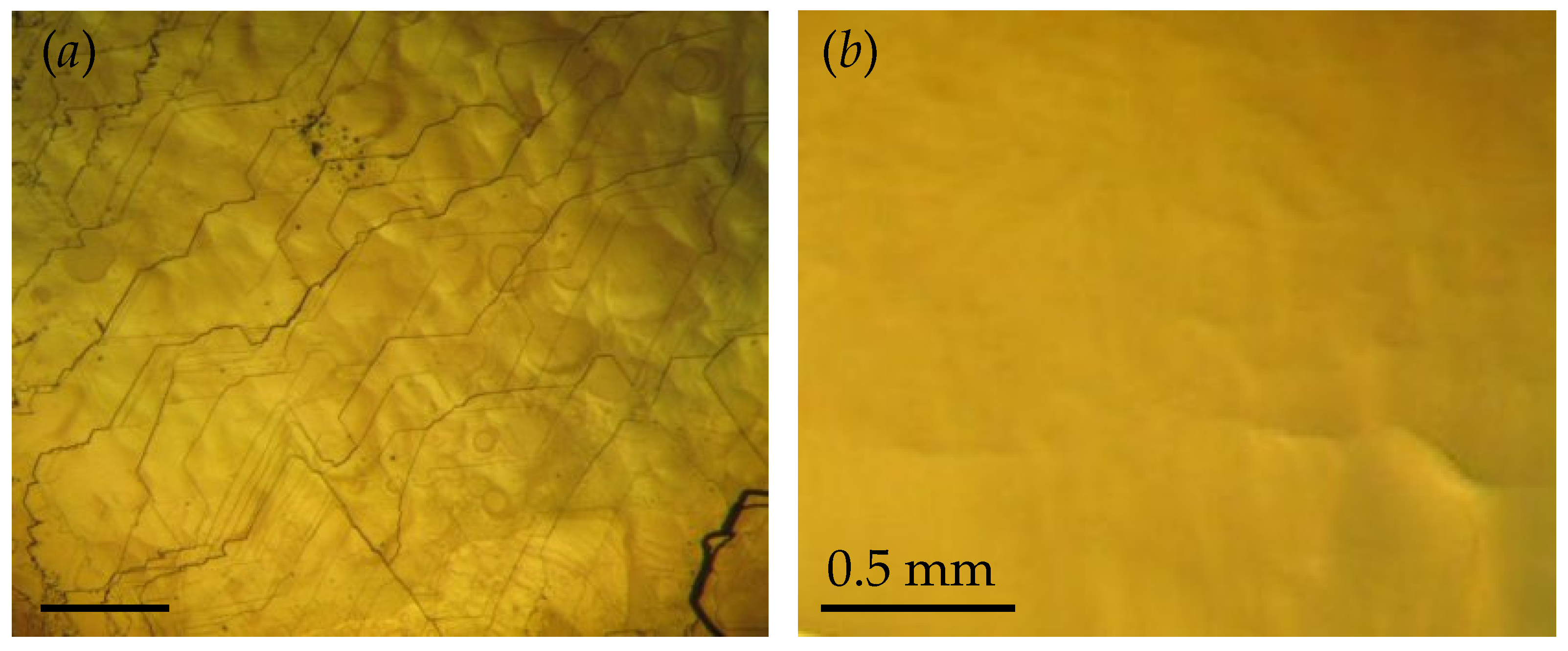
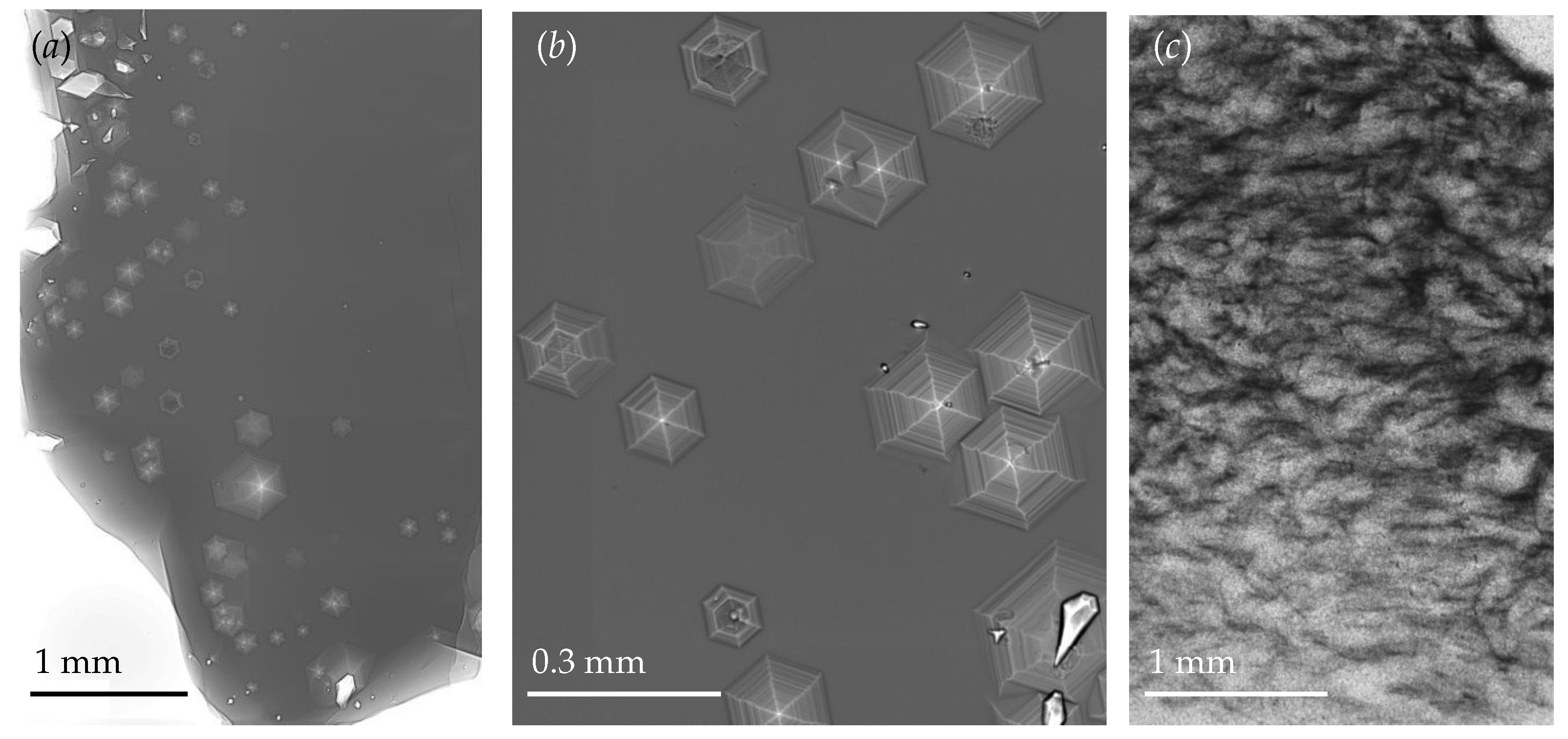
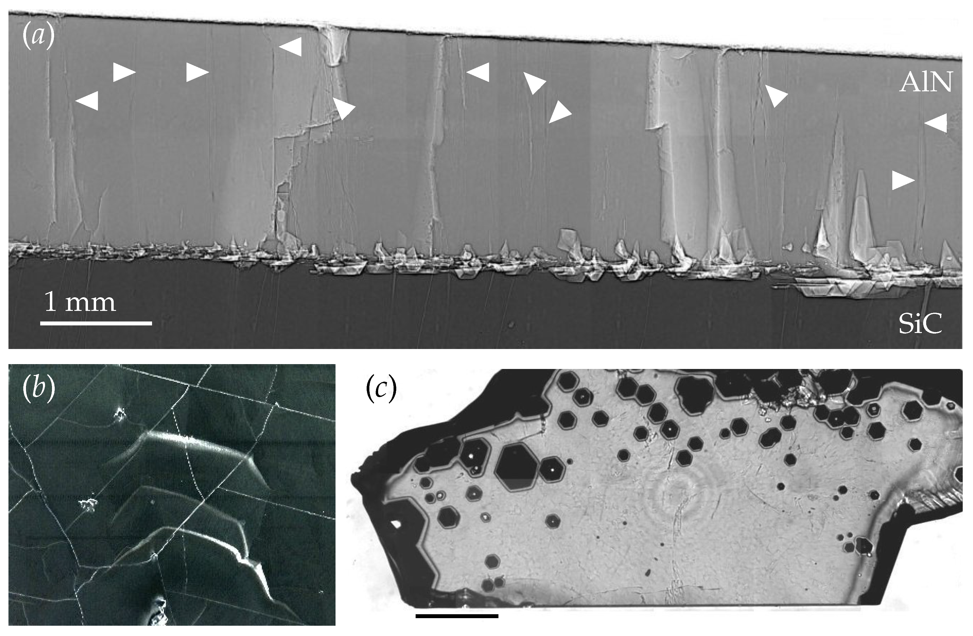
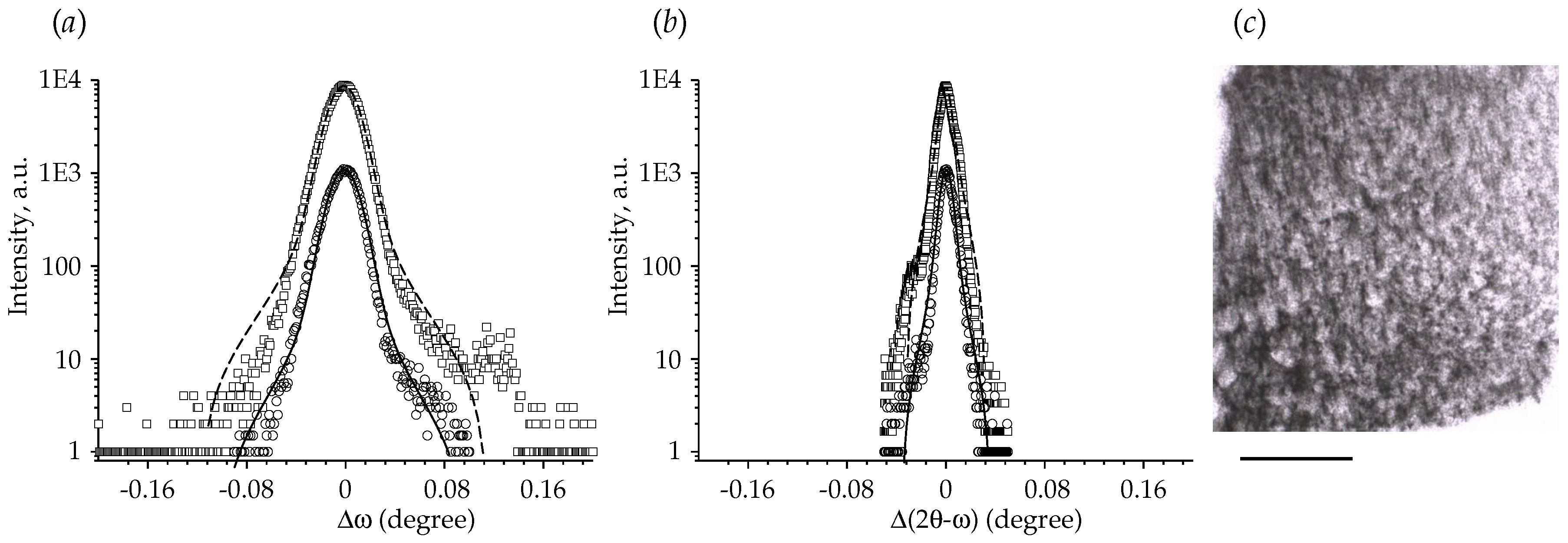
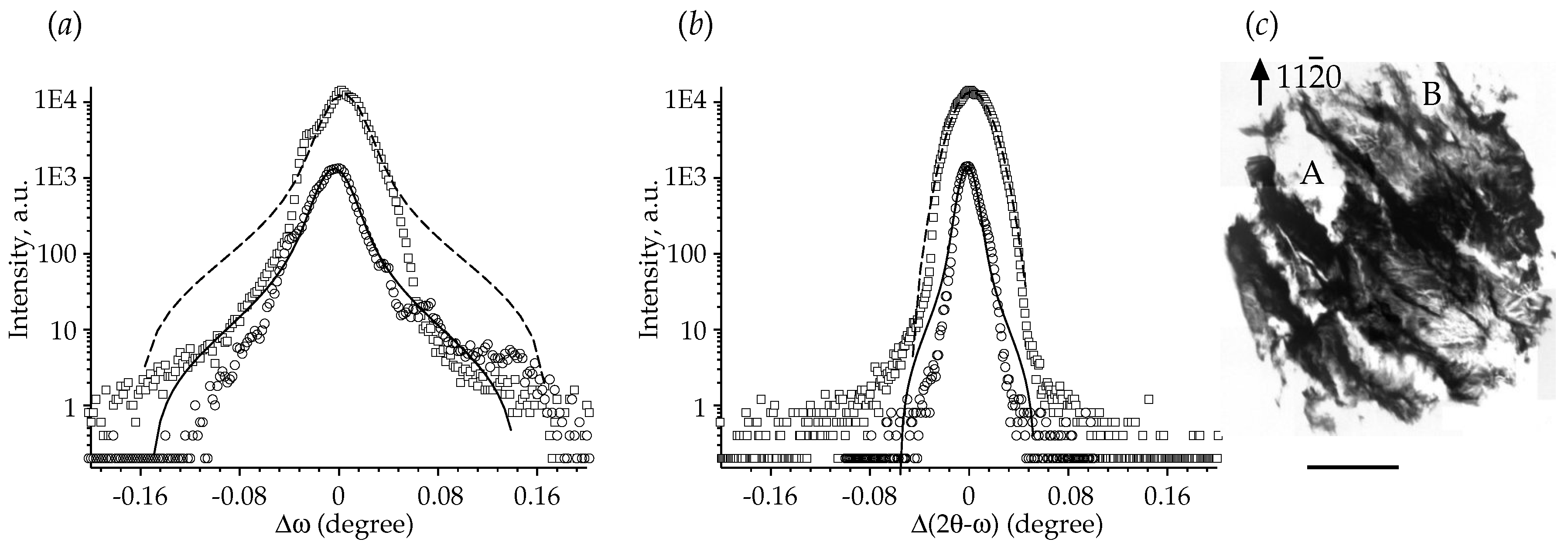
3.1. Synchrotron Imaging and X-ray Diffractometry

Our previous studies have shown that, in AlN/SiC structures cooled down from ~2000 C, cracks are always present if the ratio h 2 / h 1 ~ 1 3 , where h 1 and h 2 are the substrate and the layer thickness, respectively [13,14]. Furthermore, the critical value of the ratio, beginning from which cracking would be suppressed, was predicted to be h 2 / h 1 15 [13]. If, however, the substrate is evaporated, a freestanding AlN layer has scarce or no cracks. Figure 2 illustrates these statements, showing cracks in AlN/SiC templates in cross section (a) and in planar view (b). Figure 2a is a phase contrast image of the specimen cut parallel to the growth direction from the structure with h 2 / h 1 1 . The cracks, which are aligned perpendicular to the X-ray beam, propagate from the interface to the layer surface. We notice that the cracks have variable contrast and it changes along their lengths. Unlike surface features, which do not extend along the beam, the crack depth increases or decreases resulting in phase change and, therefore, in black or white contrast. Those cracks that have reached the surface are marked with arrows. Figure 2b is scanning electron (SEM) micrograph of the other specimen of similar thickness ratio cut perpendicularly to the growth direction. The cracks in the specimen show a typical density of 1–2 mm 2 . Figure 2c displays planar view optical micrograph of the freestanding AlN layer with 0.8 mm thickness. The layer has no cracks in the view field of 14 mm 2 but contains many microvoids located mainly along its periphery.
According to our observations, the microvoids may appear as a result of a high evaporation rate around structural defects. The pits, which are developed on dislocation outcrops during the sublimation of SiC, are very similar to the pits revealed by molten KOH etching. However, unlike the etch pits, the sublimation pits are formed on ( 000 1 ¯ ) C face rather than on (0001) Si face of SiC. The etching depth increases as the annealing time increases, and the pits eventually transform into holes. Figure 3a,b shows phase contrast images of typical microvoids enclosed in the freestanding AlN layer displayed in Figure 2c. One can also see the pores associated with the microvoids; they are polygon-shaped and grayish white. Most of the voids are located at the periphery of the crystal. This can be explained by the fact that the periphery evaporates much faster than the center. Several features are apparent in Figure 3a,b: thick borders surrounding the voids, facets, terraces and void tips. In addition to single tips, multiple tips (2–3 per void) are also present. Their origins could be associated with closely spaced dislocation outcrops. The lateral dimensions of such voids increased faster than the depth because SiC crystal evaporated predominantly in the lateral direction. We found that the lateral rate was an order of magnitude greater than the normal.
The freestanding layers that contain many microvoids usually exhibit a non-uniform dislocation structure. An example is shown in Figure 3c, which is white radiation topograph recorded from the same crystal. According to this topograph, the specimen possesses inhomogeneous spatial distribution of dislocations, which tend to be arranged in cells. We notice that the dislocation density is high enough and overlapping of their projected images cannot be avoided; it is far in excess of what could be determined using X-ray topography in transmission setting: > 10 4 10 5 cm 2 [19]. The possible conclusion from this topograph is that lattice distortion is still continuous, but dislocations tend to form boundaries between subgrains in which there is a lower dislocation density. The boundaries separate the regions of different orientations imaged in a single exposure due to the advantage of continuous radiation.
Further development of the dislocation configuration shown in Figure 3c may lead to the formation of discrete mosaic blocks. If, however, growth conditions are optimized, it is possible to obtain less inhomogeneous distribution. Let us compare two freestanding AlN layers using X-ray diffractometry and topography. One specimen (type I specimen) has neither cracks nor microvoids within the area of ~36 mm 2 . The other specimen (type II specimen) with the area of ~55 mm 2 has two cracks and about ten microvoids. Using X-ray rocking curves ( ω –scans) and longitudinal peak widths ( 2 θ ω ), we measured 0002, 0004 and 10 1 ¯ 4 reflections from these specimens. The peak widths are determined by nonlinear least-squares fits to the Voigt function, which is a convolution of a Lorentzian and a Gaussian. The full width at half height maximum (FWHM) W is calculated using the formula W = W L / 2 + W L 2 / 4 + W G 2 , where W L and W G are the Lorentzian and the Gaussian peak width, respectively.
The difference between the specimens can be seen by comparing Figure 4 and Figure 5, which display the two scans taken by symmetric 0004 and asymmetric 10 1 ¯ 4 reflections. The type I layer has broadening in 000 l reflections (~100 arcs) consistent with a screw or mixed TD density of ~ 5 × 10 5 cm 2 [2]. The defect structure of this layer causes broadening in both the symmetric and asymmetric rocking curves (Figure 4a). The 0004 and 10 1 ¯ 4 peaks have fitted widths of 96 and 92 arcs, respectively. Similar tendency is found for the type II layer, but its rocking curves are broader: 114 and 101 arcs, respectively. Additionally, multiple peaks present in the rocking curves (Figure 5a). When we compare the rocking curves with the longitudinal peaks, we see that the coupled 2 θ ω scan is very narrow for both reflections and for both types of specimens. As the crystal-analyser is set for a certain lattice parameter, the regions tilted with respect to the original region do not contribute to the width of the coupled scan. Therefore, the longitudinal peak widths are reduced significantly compared with the specimen scans. We can thus distinguish strain or dilatation from tilt or mosaic spread: both types of specimens contain larger mosaic spread and lower distribution of the lattice parameter.
By assuming the mosaic block model as a rough approximation, one can evaluate the properties that contribute to a peak width: lattice tilt, strain and subgrain size. The strain and the size (along the surface normal) effect 2 θ ω peaks. The peak width derived from the size varies as 1 / cos ω , whereas the strain contribution varies as tan ω . The ω –scan peak widths are in their turn effected by the tilt and by the subgrain size parallel to the surface, which varies as 1 / sin ω . The discrimination between the contributions is performed by plotting the direction-dependent broadening of each peak versus its location in reciprocal space [20]. There was not enough data to draw reliable conclusions since we had only two symmetrical reflections. Nevertheless, as a comparison between the specimens, we had made a rough estimate of the longitudinal strain ( ϵ ) and the out-of-plane tilt ( τ ) in the type I and type II AlN. We obtained: ϵ I = 2 × 10 4 , ϵ I I = 8 × 10 4 ; τ I = 68 arcs, τ I I = 120 arcs. For the tilt, we note that the rotation axis is parallel to 1 ¯ 2 1 ¯ 0 direction. The grain size is sometimes used to quantify dislocation densities. However, one must not use it as a measure unless the type and the distribution of dislocations is well known.
Additional information was provided by topography. Transmission setting was used to image dislocations in both materials. The dislocation density cannot be determined by topography in this case, and only the misoriented regions can be detected. A type I layer has a relatively homogeneous distribution of dislocations (Figure 4c). A type II layer shows a somewhat different distribution of dislocations and it contains large blocks (Figure 5c). The misorientation between the blocks was estimated using the incident beam divergence due to the range of wavelengths. We employed an Ru/C multilayer monochromator with an energy resolution of Δ E / E = 3 %, where E = 15 keV is principal photon energy. The width of its diffraction curve was 64 arcsec. Orientation contrast arises when a region of the crystal is misoriented by an amount larger than the beam divergence. In Figure 5c, no diffracted intensity is recorded for the regions, e.g., A and B when the Bragg condition is satisfied for most of the rest of the crystals. The angle of misorientation of each region, projected into the incidence plane, can be determined by the angle that the specimen must be rotated in order to obtain strong intensity from the region. The estimation was done in transmission as well as in reflection geometry using a Photonic Science high resolution imager. The obtained angles are in fair agreement with the value 120 arcs derived from the peak broadening analysis.
In this section, we have shown that, for both types of freestanding layers, the 2 θ ω scans are very narrow in comparison with the specimen only scans. We have obtained the values of out-of-plane tilt and longitudinal strain using the mosaic block model. However, we emphasize that other explanations of dislocation structure are possible, which will be proposed later. Additionally, it was shown that the ω and 2 θ ω scan widths were not broader for asymmetric 10 1 ¯ 4 reflection compared to symmetric 0004 reflection. From this evidence, we may conclude that each layer possesses a structure of pure edge, pure screw and/or mixed TDs. However, we note that the coplanar asymmetric reflections (such as 10 1 ¯ 4 ) are much less sensitive to edge dislocations than non-coplanar asymmetric 10 1 ¯ 3 [2] or perpendicular 10 1 ¯ 0 [6] reflections. To obtain information about pure edge TDs, we used TEM as described below.

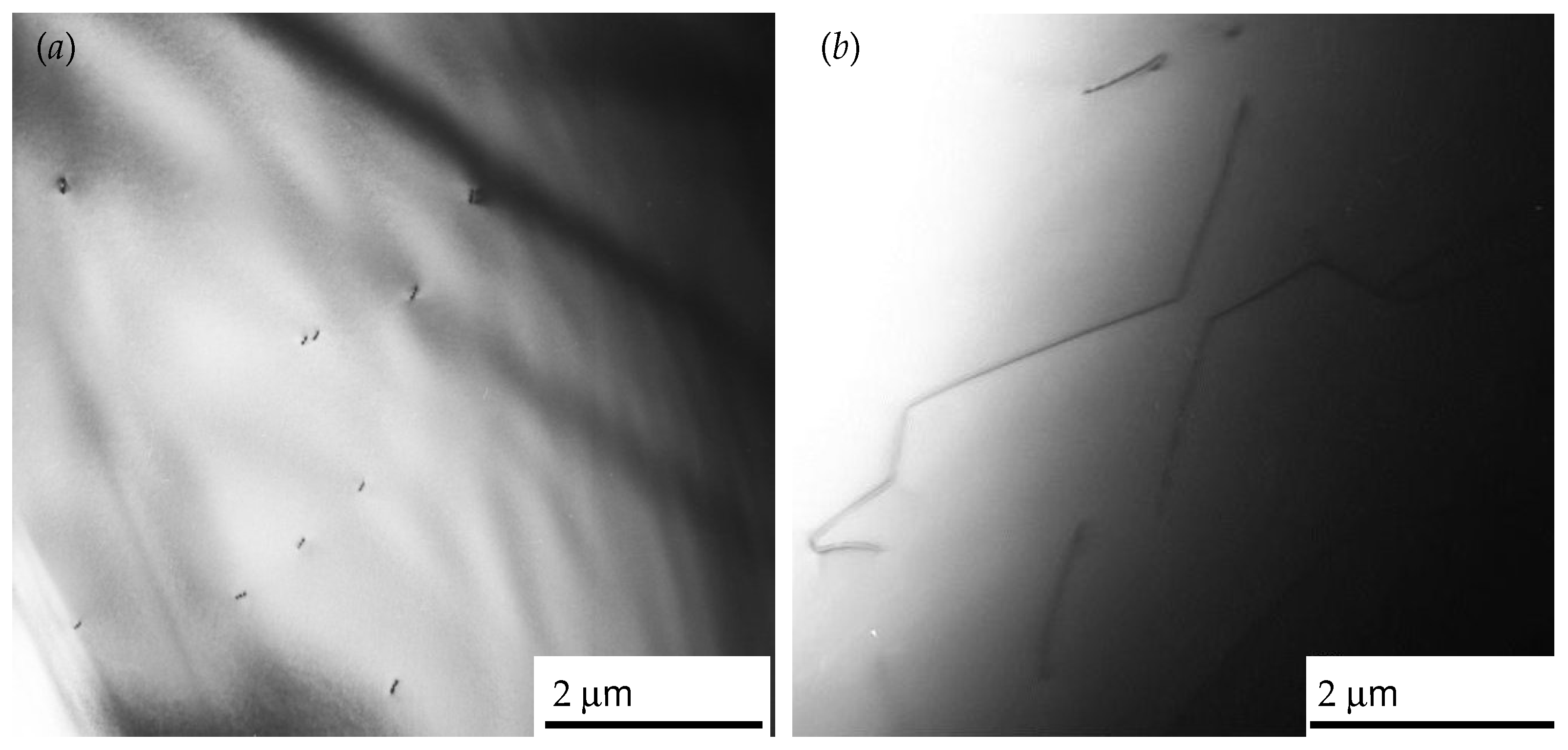
3.2. TEM Characterisation
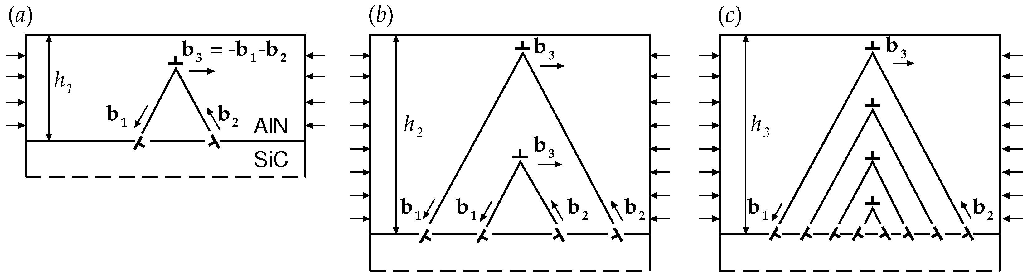
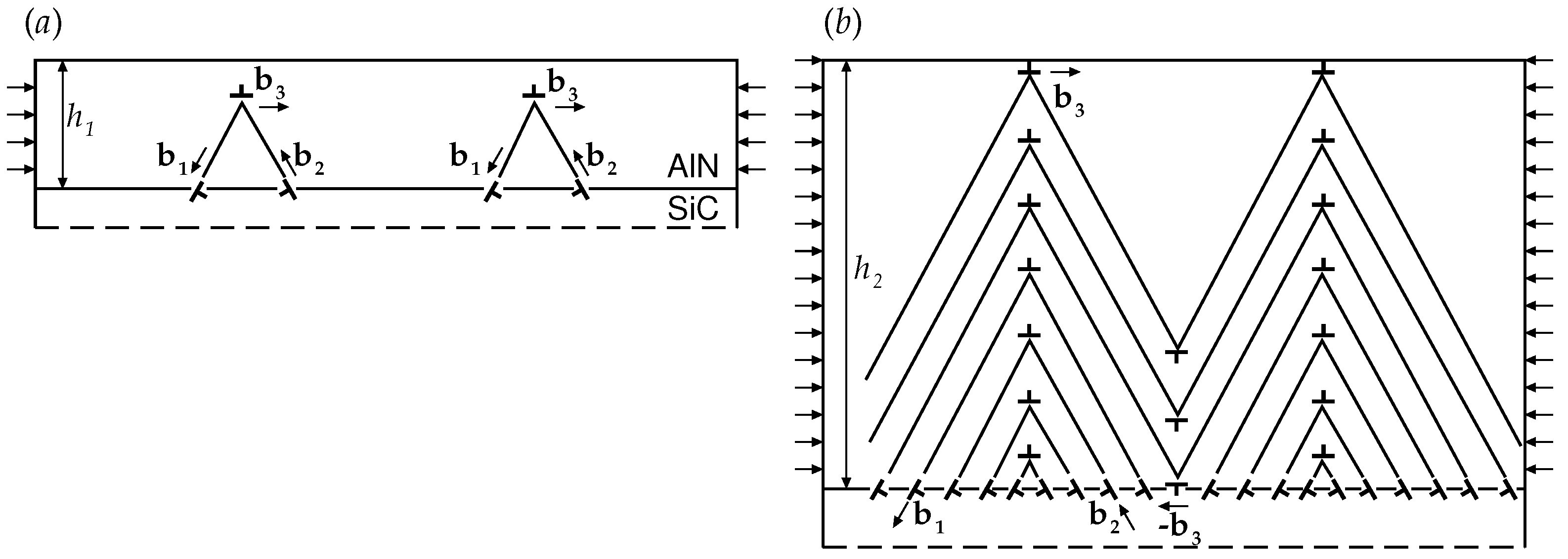
TEM investigation revealed that the dislocation structure of freestanding AlN layers generally contain discrete, randomly distributed dislocations and regular spatial arrangements of dislocations. The random arrays were observed within a few areas. They are constituted of TDs (Figure 6a), which have the lines inclined at an acute angle with respect to the 0001 direction, as well as of as-grown dislocations located in the basal plane (Figure 6b). An average density of the random configurations is relatively low because, within ~2000 μ m 2 of the sample surface, only two such regions were found. The size of each region was about 15 μ m 2 .
The regular spatial arrangements of edge TDs are well aligned along the 10 1 ¯ 0 with the linear density of ( 1.0 2.5 ) × 10 4 cm 1 ; they form low-angle tilt subgrain boundaries (Figure 7). Since the Burgers vector of a perfect dislocation located in the basal plane is 3.1 Å, the tilt angle of a subgrain with respect to the 0001 axis is about 180 arcsec (Figure 7a). This angle is reduced, provided that the dislocation line is significantly tilted from the 0001 axis (Figure 7b). In such case, the subgrain is tilted to both the 0001 axis and the axis parallel to the plane 0001 , which, in turn, causes the misorientation of the plane.

4. Discussion

The process of misfit accommodation at the early stages of epitaxial growth of AlN on SiC substrates may include the formation of rather specific dislocation arrangements. The example of the formation mechanism of TD array with 3-bilayer-high surface steps is given in Ref. [21]. In this paper, we consider the arrangements that are capable to produce misoriented subgrains in the AlN epilayers. It seems evident that TDs inherited from the substrate and growing through the epilayer can form low-energy configurations like dislocation walls and network. In this case, however, we can expect that the misorientation axes should be normal to the interface plane (0001) or slightly inclined to it. The experimental evidence of misorientation axes parallel to this plane, which is shown above, makes us search for dislocation arrangements containing long dislocation segments of edge or mixed type, which are also parallel to the interface plane.
Recently, we have suggested a theoretical model that describes the formation of so-called Λ -shaped misfit dislocation (MD) configurations in the vicinity of the AlN/SiC interface as an effective mechanism of misfit stress relaxation in the AlN layers growing on evaporated SiC substrate [15]. These configurations consist of two glide dislocation loops having one common segment of the edge type ( b 3 -dislocation) with line and Burgers vector b 3 lying in parallel with the interface (Figure 8a). Two other dislocation segments ( b 1 - and b 2 -dislocations), which are parallel to the interface, are, in fact, the MD segments, while four other dislocation segments are inclined to the interface and can be considered as TDs. The generation and extension of such Λ -shaped MD configurations along the interface causes the misfit stress relaxation [15] and may lead to formation of very long segments of b 3 -dislocations placed in the bulk of the AlN layer. A number of such long dislocation segments arranged periodically in the same ‘vertical’ plane (normal to the interface plane) would give a dislocation wall that is a tilt low-angle boundary with the orientation axis parallel to the interface plane.
It is easy to see that such a wall composed of b 3 -dislocations could result from repeated events of Λ -shaped MD configuration formation (Figure 8b,c). Indeed, the first Λ -shaped MD configuration, which is generated when the layer thickness h = h 1 becomes bigger than a critical thickness h c , creates some additional compression on the AlN layer surface over the first b 3 -dislocation, so that this place must be the most favorable site for nucleation of a new Λ -shaped MD configuration (Figure 8b) according to the mechanism described in Ref. [15]. Obviously, the second Λ -shaped MD configuration must be formed over the first one, at h = h 2 > h 1 . As a result, after a set of similar repeated events, we can obtain a ‘matrioshka’ of a number of Λ -shaped MD configurations repeatedly generated over each other (Figure 8c).
In the case when two Λ -shaped MD configurations are generated simultaneously and are not too far from each other (Figure 9a), they can develop in a common dislocation arrangement, forming two misoriented domains (subgrains). Indeed, when the distance between two forming ‘matrioshkas’ becomes smaller than the layer thickness, we can expect that some b 1 - and b 2 -dislocations belonging to these ’matrioshkas’ can react and produce new edge dislocations with Burgers vector b 1 + b 2 = –b 3 (Figure 9b). As a result, two side walls of b 3 -dislocations and one central wall of b 3 -dislocations form three tilt low-angle boundaries, which, in fact, border two subgrains.
Thus, the processes of misfit stress relaxation, which occur through the generation of Λ -shaped MD configurations and their natural transformation during the AlN growth to ’matrioshkas’, composed of such Λ -shaped MD configurations formed over each other, can be accompanied with formation of misoriented domains (subgrains) with misorientation axes parallel to the interface plane.

5. Conclusions

Freestanding AlN layers were fabricated by an SiC substrate evaporation method. The continuity of the layers has been significantly improved by this method, which allowed us to investigate the distribution of dislocations close to the former interface between AlN and SiC. In agreement with previous studies, we observed the broadening in 000 l reflections. The amount of broadening was consistent with the pure screw and/or mixed TD densities observed earlier in good quality parts of AlN bulk crystals grown on SiC seeds. Using scans along two directions in reciprocal space we found that the freestanding layers contained larger mosaic spread and lower distribution of strain. Thus, the dislocations arranged to form low-angle subgrain boundaries. Edge TD arrays along 10 1 ¯ 0 directions were revealed by TEM. Such arrays were localized only in certain places rather than crossed the total thickness throughout the entire crystal. The evidence from X-ray topography presented a picture of a fairly uniform dislocation distribution. Non-uniform configurations contained large-size subgrains with relatively low misorientations: ~120 arcs.
We have shown that, in comparison with earlier studies of thin-layer AlN/SiC templates, the structural quality of freestanding layers is improved. However, defects located in the substrates give rise to higher evaporation rate, which causes the formation of microvoids and pores in the growing layers. Such evaporation behavior of SiC tends to affect both the dislocation distribution and the dislocation density. We conclude that the structural quality can be improved more markedly, provided the substrate evaporation is performed appropriately and provided the growth conditions are optimized. Since no mechanism responsible for the relaxation of misfit stress in AlN/SiC has been proposed so far, we have suggested a suitable model by which we can explain our experimental observations.

Acknowledgments

Jung Ho Je acknowledges the support of the Ministry of Trade, Industry and Energy (MOTIE) and the Korea Institute for Advancement of Technology (KIAT) through the International Cooperative R & D Program. The support includes covering the costs to publish in open access. Mikhail Gutkin acknowledges the support of the Ministry of Education and Science of the Russian Federation (Grant No. 3.3194.2017/PCh). Evgeniy Mokhov acknowledges the support of the Russian Science Foundation (Grant RSF No. 16-42-01098). TEM investigation has been carried out with the use of equipment of the Federal Joint Research Centre “Material science and characterization in advanced technology” in the Ioffe Institute.

Author Contributions

Tatiana Argunova and Jung Ho Je performed the synchrotron X-ray imaging experiments; Mikhail Gutkin and Kristina Mikaelyan elaborated on the theory; Alexander Kalmykov, Alexander Myasoedov and Lev Sorokin conducted the TEM experiments and analyzed the data; Olga Kazarova and Evgeniy Mokhov provided the freestanding AlN crystals and investigated the SiC evaporation process; Kirill Shcherbachev did the XRD measurements; and Tatiana Argunova and Mikhail Gutkin contributed equally by writing the manuscript.

Conflicts of Interest

The authors declare no conflict of interest.

References

  1. Hartmann, C.; Wollweber, J.; Dittmar, A.; Irmscher, K.; Kwasniewski, A.; Langhans, F.; Neugut, T.; Bickermann, M. Preparation of bulk AlN seeds by spontaneous nucleation of freestanding crystals. Jpn. J. Appl. Phys. 2013, 52, 08JA06-1–08JA06-6. [Google Scholar] [CrossRef]
  2. Sumathi, R.; Gille, P. Development and progress in bulk c-plane AlN single-crystalline template growth for large-area native seeds. Jpn. J. Appl. Phys. 2013, 52, 08JA02-1–08JA02-4. [Google Scholar] [CrossRef]
  3. Dalmau, R.; Moody, B.; Xie, J.; Collazo, R.; Sitar, Z. Characterization of dislocation arrays in AlN single crystals grown by PVT. Phys. Status Solidi A 2011, 208, 1545–1547. [Google Scholar] [CrossRef]
  4. Zhou, T.; Raghothamachar, B.; Wu, F.; Dalmau, R.; Moody, B.; Craft, S.; Schlesser, R.; Dudley, M.; Sitar, Z. Characterization of threading dislocations in PVT-grown AlN substrates via X-ray topography and ray tracing simulation. J. Electron. Mater. 2014, 43, 838–842. [Google Scholar] [CrossRef]
  5. Herro, Z.; Zhuang, D.; Schlesser, R.; Sitar, Z. Growth of AlN single crystalline boules. J. Cryst. Growth 2010, 312, 2519–2521. [Google Scholar] [CrossRef]
  6. Miyanaga, M.; Mizuhara, N.; Fujiwara, S.; Shimazu, M.; Nakahata, H.; Kawase, T. Evaluation of AlN single-crystal grown by sublimation method. J. Cryst. Growth 2007, 300, 45–49. [Google Scholar] [CrossRef]
  7. Nagai, I.; Kato, T.; Miura, T.; Kamata, H.; Naoe, K.; Sanada, K.; Okumura, H. AlN bulk single crystal growth on 6H-SiC substrates by sublimation method. J. Cryst. Growth 2010, 312, 142–149. [Google Scholar] [CrossRef]
  8. Mokhov, E.; Izmaylova, I.; Kazarova, O.; Wolfson, A.; Nagalyuk, S.; Litvin, D.; Vasiliev, A.; Helava, H.; Makarov, Y. Specific features of sublimation growth of bulk AlN crystals on SiC wafers. Phys. Status Solidi C 2013, 10, 445–448. [Google Scholar] [CrossRef]
  9. Kaganer, V.M.; Brandt, O.; Trampert, A.; Ploog, K.H. X-ray diffraction peak profiles from threading dislocations in GaN epitaxial films. Phys. Rev. B 2005, 72, 045423. [Google Scholar] [CrossRef]
  10. Wolfson, A. Spontaneous detachment of a sublimation-grown AlN layer from an SiC-6H substrate. Semiconductors 2009, 43, 818–819. [Google Scholar] [CrossRef]
  11. Dalmau, R.; Schlesser, R.; Rodriguez, B.J.; Nemanich, R.J.; Sitar, Z. AlN bulk crystals grown on SiC seeds. J. Cryst. Growth 2005, 281, 68–74. [Google Scholar] [CrossRef]
  12. Yamakawa, M.; Murata, K.; Iwaya, M.; Takeuchi, T.; Kamiyama, S.; Akasaki, I.; Amano, H.; Azuma, M. Freestanding highly crystalline single crystal AlN substrates grown by a novel closed sublimation method. APEX 2011, 4, 045503-1–045503-3. [Google Scholar] [CrossRef]
  13. Argunova, T.S.; Gutkin, M.Y.; Mokhov, E.N.; Kazarova, O.P.; Lim, J.-H.; Scheglov, M.P. Prevention of AlN crystal from cracking on SiC substrates by evaporation of the substrates. Phys. Solid State 2015, 57, 2473–2478. [Google Scholar] [CrossRef]
  14. Argunova, T.S.; Gutkin, M.Y.; Kazarova, O.P.; Mokhov, E.N.; Nagalyuk, S.S.; Je, J.H. Synchrotron X-ray study on crack prevention in AlN crystals grown on gradually decomposing SiC substrates. In Silicon Carbide and Related Materials; Chaussende, D., Ferro, G., Eds.; Trans. Tech. Publications Ltd.: Zürich, Switzerland, 2015; Volume 821–823, pp. 1011–1014. [Google Scholar]
  15. Argunova, T.S.; Gutkin, M.Y.; Shcherbachev, K.D.; Je, J.H.; Lim, J.-H.; Kazarova, O.P.; Mokhov, E.N. Microstructure and strength of AlN-SiC interface studied by synchrotron X-rays. J. Mater. Sci. 2017, 52, 4244–4252. [Google Scholar] [CrossRef]
  16. Avdeev, O.V.; Chemekova, T.Y.; Mokhov, E.N.; Nagalyuk, S.S.; Helava, H.; Ramm, M.G.; Segal, A.S.; Zhmakin, A.I.; Makarov, Y.N. Development of 2 inch AlN Substrates Using SiC Seeds. In Modern Aspects of Bulk Crystal and Thin Film Preparation; Kolesnikov, N., Ed.; InTech: Rijeka, Croatia, 2012; pp. 213–262. [Google Scholar]
  17. Epelbaum, B.M.; Heimann, P.; Bickermann, M.; Winnacker, A. Comparative study of initial growth stage in PVT growth of AlN on SiC and on native AlN substrates. Phys. Status Solidi C 2005, 2, 2070–2073. [Google Scholar] [CrossRef]
  18. Stein, R.A.; Lanig, P.; Leibenzeder, S. Influence of surface energy on the growth of 6H-SiC and 4H-SiC polytypes by sublimation. Mater. Sci. Eng. 1992, B11, 69–71. [Google Scholar] [CrossRef]
  19. Bowen, D.K.; Tanner, B.K. High Resolution X-ray Diffractometry and Topography; Taylor & Francis Ltd.: London, UK, 1998. [Google Scholar]
  20. Birkholz, M. Thin Film Analysis by X-ray Scattering; Wiley-VCH Verlag GmbH and Co., KGaA: Weinheim, Germany, 2006. [Google Scholar]
  21. Okumura, H.; Kimoto, T.; Suda, J. Formation mechanism of threading-dislocation array in AlN layers grown on 6H-SiC (0001) substrates with 3–Bilayer-high surface steps. Appl. Phys. Lett. 2014, 105, 071603-1–071603-4. [Google Scholar] [CrossRef]
Figure 1. Optical micrographs (in reflected light) of SiC substrate 8 mm in diameter after annealing in AlN vapor during 4 h. (a) C face; (b) Si face. Annealing temperature is 1880 C; N 2 pressure is 0.1 Bar.
Crystals 07 00163 g001
Figure 2. (a) Synchrotron X-ray phase contrast image of AlN/SiC template in cross section view. White arrows highlight the locations of cracks; (b) SEM image of AlN/SiC template in planar view. Field width 2 mm; (c) optical micrograph (in reflection light) of freestanding AlN layer. Scale bar 1 mm.
Crystals 07 00163 g002
Figure 3. (a,b) SR X-ray phase contrast images of freestanding AlN layer shown in Figure 2c. The voids are imaged at a distance of 17 cm behind the specimen; (c) SR X-ray diffraction topograph of the same specimen recorded using white radiation in transmission setting. Film Kodak SR45.
Crystals 07 00163 g003
Figure 4. Superimposed symmetric and asymmetric ω and 2 θ ω X-ray diffraction peaks for type I layer of AlN. (a) X-ray rocking curves ( ω –scans) from 0004 (squares) and 10 1 ¯ 4 (circles) reflections. Log scale. The peaks have fitted widths of 96 and 92 arcsec, respectively. Voight fit is shown by dashed and solid lines; (b) ( 2 θ ω ) scans from 0004 and 10 1 ¯ 4 reflections. The peaks have fitted widths of 38 and 39 arcs, respectively; (c) X-ray topograph of a type I layer taken using white radiation in transmission setting. Film Kodak SR45. Scale bar 0.8 mm.
Crystals 07 00163 g004
Figure 5. Superimposed ω and 2 θ ω scans for type II layer of AlN. (a) ω –scans from 0004 (squares) and 10 1 ¯ 4 (circles) reflections. Log scale. The peaks have fitted widths of 114 and 101 arcsec, respectively. Voight fit is shown by dashed and solid lines; (b) ( 2 θ ω ) scans from 0004 and 10 1 ¯ 4 reflections. The peaks have fitted widths of 110 and 51 arcsec, respectively; (c) X-ray diffraction topograph of type II layer taken with 11 2 ¯ 0 reflection using monochromatic radiation with principal photon energy E = 15 keV. Scale bar 2 mm. Photonic Science VHR.
Crystals 07 00163 g005
Figure 6. Plan view TEM image (zone axis) of threading dislocations (a) and dislocations in the basal plane (b).
Crystals 07 00163 g006
Figure 7. (a) an 10 1 ¯ 0 array of threading dislocations; (b) dislocation lines significantly tilted from the 0001 axis.
Crystals 07 00163 g007
Figure 8. Theoretical model of the formation of a number of Λ -shaped misfit dislocation configurations in the vicinity of the AlN/SiC interface, which produce a vertical wall of b 3 -dislocations (a tilt low-angle boundary) and two horizontal walls of b 1 - and b 2 -dislocations. (a) the first Λ -shaped MD configuration generated at h = h 1 > h c as described in Ref. [15]; (b) the second Λ -shaped MD configuration generated in a similar way over the first one in the region of extra compression created by the first b 3 -dislocation at h = h 2 > h 1 ; (c) a ‘matrioshka’ of a number of Λ -shaped MD configurations repeatedly generated over each other at h = h 3 > h 2 .
Crystals 07 00163 g008
Figure 9. Theoretical model of the formation of misoriented domains separated from each other by tilt low-angle boundaries composed of ± b 3 -dislocations in an AlN layer on an SiC substrate. (a) a couple of neighboring Λ -shaped MD configurations in the vicinity of the AlN/SiC interface, generated at h = h 1 > h c as described in Ref. [15]; (b) two neighboring ’matrioshkas’ of Λ -shaped MD configurations in contact, separated by a wall of b 3 -dislocations accidentally created in reactions of meeting b 1 - and b 2 -dislocations at h = h 2 > > h 1 .
Crystals 07 00163 g009

