Interfacial Mixing Analysis for Strained Layer Superlattices by Atom Probe Tomography
by
 ,
,
Ayushi Rajeev
1 ,
,
Weixin Chen
2,
Jeremy D. Kirch
1,
Susan E. Babcock
2,
Thomas F. Kuech
3,
Thomas Earles
4 and
Luke J. Mawst
1,* 1
Department of Electrical and Computer Engineering, University of Wisconsin-Madison, Madison, WI 53706, USA
2
Department of Material Science and Engineering, University of Wisconsin-Madison, Madison, WI 53706, USA
3
Department of Chemical and Biological Engineering, University of Wisconsin-Madison, Madison, WI 53706, USA
4
Intraband LLC, 505 S. Rosa Road, Suite 34, Madison, WI 53719, USA
*
Author to whom correspondence should be addressed.
Crystals 2018, 8(11), 437; https://doi.org/10.3390/cryst8110437
Submission received: 30 October 2018
/
Revised: 17 November 2018
/
Accepted: 18 November 2018
/
Published: 21 November 2018
(This article belongs to the Special Issue MOVPE Growth of Crystalline Film)
Abstract
:Quantum wells and barriers with precise thicknesses and abrupt composition changes at their interfaces are critical for obtaining the desired emission wavelength from quantum cascade laser devices. High-resolution X-ray diffraction and transmission electron microscopy are commonly used to calibrate and characterize the layers’ thicknesses and compositions. A complementary technique, atom probe tomography, was employed here to obtain a direct measurement of the 3-dimensional spatially-resolved compositional profile in two InxGa1−xAs/InyAl1−yAs III-V strained-layer superlattice structures, both grown at 605 °C. Fitting the measured composition profiles to solutions to Fick’s Second Law yielded an average interdiffusion coefficient of 3.5 × 10⁻²³ m2 s−1 at 605 °C. The extent of interdiffusion into each layer determined for these specific superlattices was 0.55 nm on average. The results suggest that quaternary active layers will form, rather than the intended ternary compounds, in structures with thicknesses and growth protocols that are typically designed for quantum cascade laser devices.

1. Introduction
Quantum cascade laser (QCL) devices employ conduction band engineering to obtain a desired emission wavelength. Typically, they contain active regions consisting of 30–40 repetitions of a complex motif composed of quantum wells and barriers of various compositions and thicknesses in the range of 1–5 nm each [1]. A desirable feature of QCLs, being intersubband transition devices, is the tunability of the emission wavelength through the design of the thickness and composition of each layer within a chosen material system. However, these structures are sensitive to small deviations from the designed thicknesses and compositions, which can alter the emission wavelength through changes in the electron wavefunctions in the conduction band [2]. Moreover, for strain-compensated superlattices (SLs), minor thickness variations can lead to an imbalance in the overall strain-thickness product, which may result in strain relaxation in the several-microns-thick active region.
Simulations of experimental X-ray data are typically used to calibrate the growth process, and to assess the integrity of the final device structure. These simulations can provide an accurate measurement of the periodicity of the SL and the composition of the motif averaged over its volume. However, they provide rather little insight into the composition profile within the motif, which is critical to device performance, as the same high-resolution X-ray diffraction (HRXRD) data typically can be fit with the same accuracy with several composition profiles that have the same periodicity and average composition as the sample [3].
Transmission electron microscopy (TEM) provides details of the atomic structures of the layers and interfaces, most readily in 2D projections [4]. Near-atomic-resolution compositional mapping in three dimensions is more challenging in TEM. These shortcomings in the analysis of QCL structures are addressed in this study by utilizing atom probe tomography (APT) as a complementary technique to assess InGaAs/InAlAs strained-bilayer SL structures grown by organometallic vapor phase epitaxy (OMVPE). Profiles of the In, Al, and Ga concentrations in the growth direction elucidate the compositional sharpness of the interfaces in two strained-layer SLs. Prior studies of this type on a nominally lattice-matched SL explained the red-shifted emission wavelength for QCLs on InP [2].
2. Materials and Methods
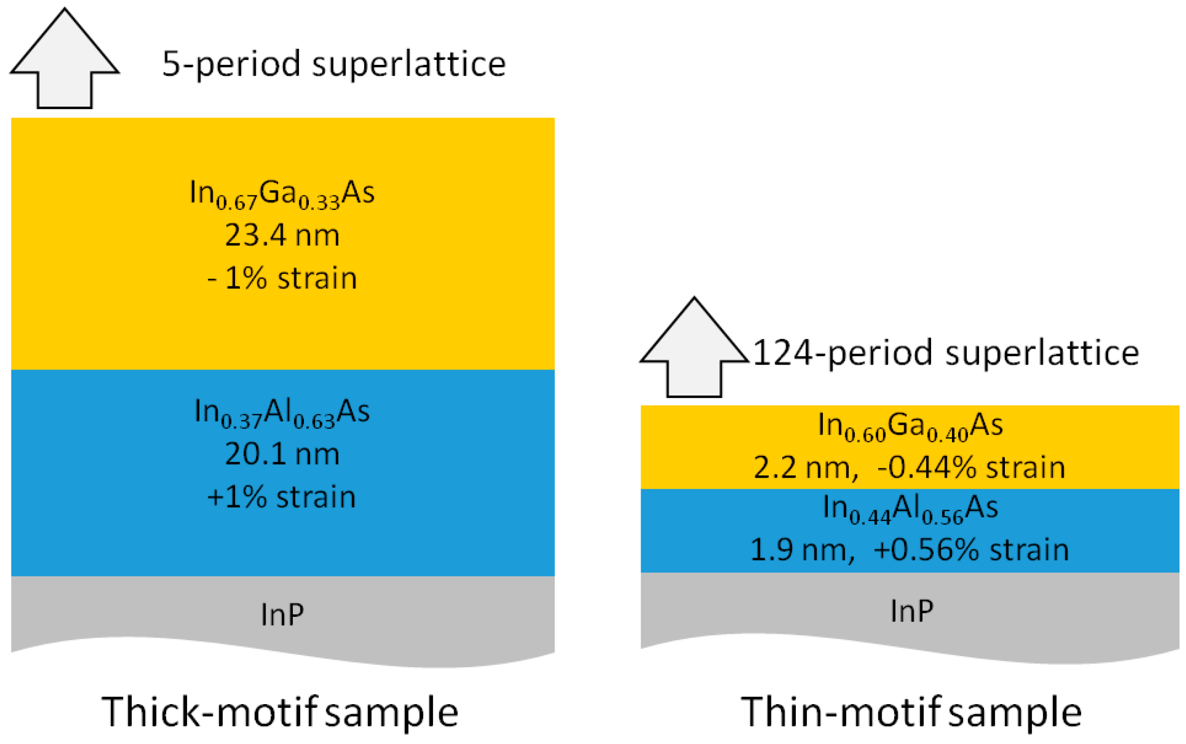
In1−xGaxAs/In1−yAlyAs strained SL samples with the target characteristics illustrated in Figure 1 were grown on (001)-oriented InP substrates. The sample designs included a thick (43.5 nm) motif SL composed of five repetitions of In0.37Al0.63As (20.1 nm)/In0.67Ga0.33As (23.4 nm) with 1% tensile/compressive strain relative to the InP substrate, nominally and respectively, and a thin (4.1 nm)-motif SL composed of 124 repetitions of In0.44Al0.56As (1.9 nm)/In0.6Ga0.4As (2.2 nm) nominally strained +0.56%/−0.47% relative to the substrate, respectively.
Both SL samples were grown in a close-coupled showerhead reactor at a reactor pressure of 100 Torr and at a temperature of 605 °C, with a wafer rotation of 100 rpm. The growth rates and V:III precursor ratios are listed in Table 1. The interruption time for switching between the SL layers was 5 s. Trimethylgallium, trimethylindium, trimethylaluminum, arsine, and phosphine comprised the precursors.
Taking into account the total volume upstream of the susceptor and the total precursor fluxes, which are dominated by the hydrogen carrier gas, the calculated precursor residence time was about 0.4 s, well below the interruption time of 5 s. These growth procedures resulted in the first-to-be-grown layers of the thick-motif SL being annealed at 605 °C for approximately 1900 s (about 32 min), and in the thin-motif SL for 5700 s (about 95 min).
The structural and microstructural characteristics of these two SLs were investigated using HRXRD and APT. ω-2θ X-ray diffraction patterns about the (004) diffracted beam were obtained at a step size of 0.002° using a PANalytical X’pert materials research diffractometer (MRD) equipped with as Ge (220) monochromator on the source side. The atom probe data were obtained using a LEAP 3000X Si local electrode atom probe. Needle-shaped atom probe specimens were prepared using conventional focused-ion-beam (FIB) lift-out and sharpening methods [5]. A 30 kV Ga+ beam was used for cutting, mounting, and initial shaping of the specimens; a 2 kV, 100 pA Ga+ beam was used for final sharpening. The long axis of the specimens was approximately parallel to the [001] growth direction of the SL and the z-axis of atom probe tomographs.
Atom probe data were obtained in the pulsed-laser mode at a laser pulse rate of 400 kHz, an ion detection rate of 0.5%, and with the specimen holder cooled to 54 K. The laser pulse energy was 8 pJ for the thick-motif SL specimen, and 13 pJ for the thin-motif specimen for which results are presented below. Field evaporation commenced at a direct current (DC) voltage of ~2600 V for both of these specimens. The voltage increased to ~3200 V before the each of the specimens fractured. CAMECA’s IVAS ™ [6] software suite was used to produce and to interrogate the reconstructions. Data were obtained from the bottom 1.5 bilayers and the substrate of the thick-motif SL, and ~70 repetitions of the thin-motif SL. Because a voltage drop was associated with crossing the interface between the (InAl)As/(InGa)As SL and the InP substrate, shank-angle evolution was used to calibrate the reconstructions. The initial specimen tip radii and shank angles were determined from secondary-electron SEM images of the specimens, prior to running them in the atom probe. The resolution of the APT data in the growth direction is expected to be better than that in the lateral direction [7]. The resolution in the growth direction could approach 0.2 nm in this analysis. The motif thicknesses in the reconstruction were within 10% of the periodicity deduced from the HRXRD diffraction pattern of each sample. Thus, the atom probe data might underestimate the diffusion distance that is determined below by at most 10%. The atom number density obtained in the reconstruction matched that determined for unstrained materials, assuming that Vegard’s law holds, to within 15%. These comparisons were used to validate the reconstruction parameters. Atom probe data were obtained from interior sections of the thin-motif SL only, but shank-angle evolution was nevertheless employed for consistency.
3. Results
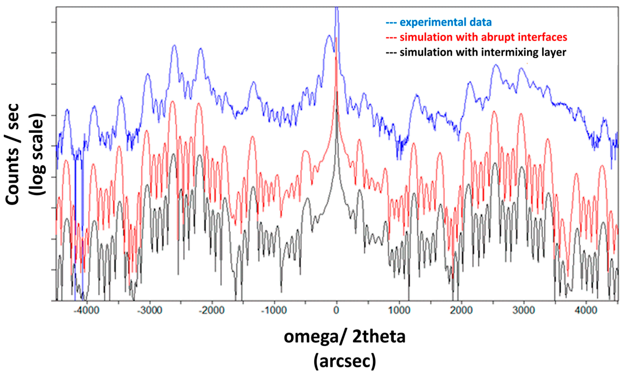
Figure 2 presents the HRXRD pattern measured from the thick-motif SL and two simulated patterns. The experimental pattern shows the sharp oscillations indicative of a highly periodic structure in the [001] (growth) direction, implying that the composition profile is repeated exactly in each bilayer motif, and that the interfaces between the component materials are planar. The shoulder at the lower side of the central InP substrate peak is due to an average residual, 0.093% compressive strain in the superlattice, which is not seen in the simulation for the targeted strain compensated superlattice. The simulations indicate a total motif thickness of 43.5 nm.
For the computed X-ray diffraction patterns shown in Figure 2, both assume the same total thickness of the superlattice motif and the same average composition within the motif. The simulations differ in how the component elements are distributed within the motif. The red curve simulates the diffraction pattern from a superlatttice motif, with step function changes in concentrations of the component elements at discrete interfaces between the sublayer, each of which has a uniform but different chemical composition. The black curve simulates the interfaces (simulation 2) as additional layers of thickness 1 nm with an intermediate composition, In0.52Al0.315Ga0.165As, and keeps the periodicity of the motif constant. The figure demonstrates that the distance over which the composition change occurs, and therefore the interface thickness, cannot be deduced from this X-ray diffraction experiment, due to the subtlety of the changes that the different composition profiles induce in the simulated pattern. However, the thickness of the bilayer motif and its average composition can be determined from the HRXRD pattern, and has served as inputs into the calibration of the atom probe data reconstruction.
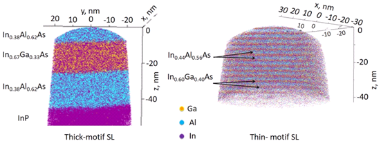
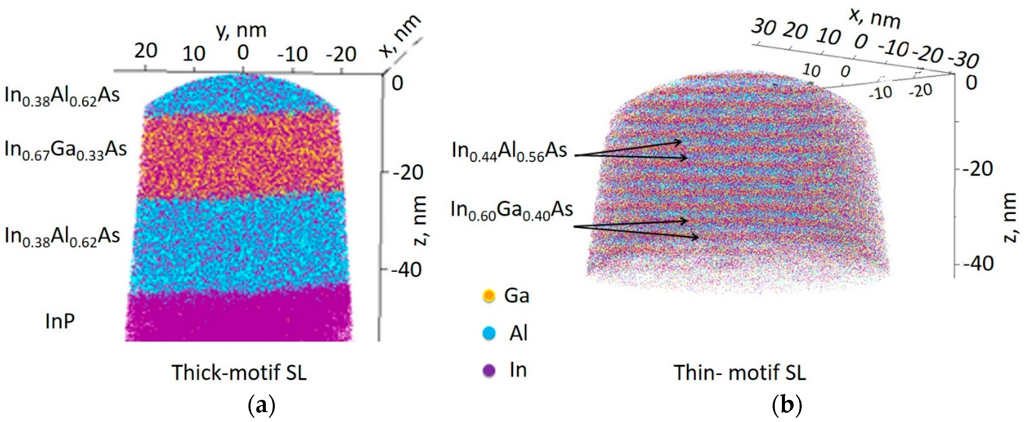
The atom maps constructed from the atom probe data are shown in Figure 3. The layer compositions were deduced by fixing the As concentration at 50 at.%, are In0.39Al0.61As/In0.69Ga0.31As, which were close to the values obtained from HRXRD (Table 2). Confidence in the magnification calibration of the atom probe reconstruction in the growth direction, that is, perpendicular to the interfaces, was of particular importance. The reconstruction parameters were tuned such that the layers in the reconstruction were planar and the period of the SL was within 10% deviation from the value deduced by HRXRD. A ±1% uncertainty was observed in the HRXRD fit for this SL.
Concentration profiles along the growth direction and perpendicular to the interfaces were deduced from the atom probe reconstructions, in order to measure the compositional width of the interfaces. A cylindrical volume-shaped subset of the reconstruction (a “region of interest”) centered approximately along the long axis of the specimen was extracted for this analysis, in order to exclude possible surface-related artifacts and distortions. An iso-concentration surface located approximately at one of the interfaces was chosen as the zero for these profiles. The compositions of sequential 0.2 nm thick discs of radius 9 nm lying parallel to the iso-concentration surface were determined from the reconstruction to generate the concentration profile (a “proxigram”). Extracting the concentration profile in this way should minimize any artificial broadening of the interface due to steps or other local morphological features with sizes greater than 0.5 nm. Growth steps up to 0.5 nm (or equivalently one unit cell) would be averaged in this method.
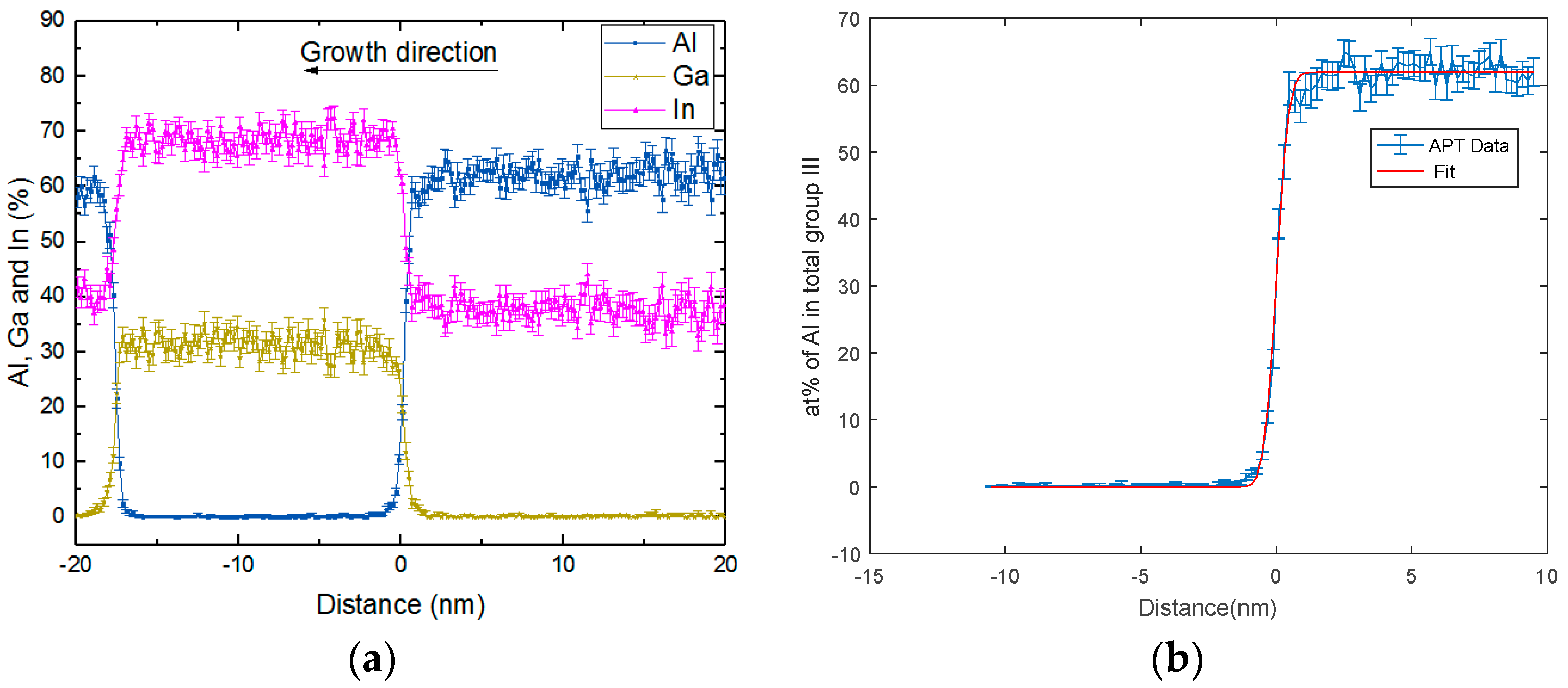
Figure 4a shows proxigrams for the relative concentrations of the group III elements for the thick-motif SL. The III:V ratios deduced from the atom probe data were of the order (53:47), rather than 1:1. This deviation from the known stoichiometry of III-V compounds is commonly observed in atom probe reconstructions of arsenides and phosphides, and is believed to arise from the propensity for As and P to field evaporate as poly-atomic ions [5]. Because compound semiconductors are essentially line compounds with a III:V ratio of 1:1, the As concentration was assumed to be equal to 50 at.% throughout both superlattices, and the sum of the group III concentrations was set to 100%, to be consistent with the chemical formula as typically written, throughout the profiles shown in Figure 4 and Figure 5.
4. Discussion
4.1. Extent of Interfacial Mixing in the Thick-Motif Sample
To assess the extent of intermixing at the interfaces between component materials, and to extract a measure of the compositional width of the interfaces, solutions to Fick’s second law were fit to the measured concentration profiles. For both the thick-motif and the thin-motif SLs, the interdiffusion coefficient, D, was assumed to be independent of composition. In the case of the thick-motif sample, mass spectra corresponding to the central volume of the (InAl)As showed no peaks corresponding to Ga; in parallel, mass spectra from the central volume of the InGaAs layers showed no intensity at the Al ion positions. Therefore, the one-dimensional solution to Fick’s second law for a diffusion couple composed of two semi-infinite solids was fit to the Al concentration profile to extract a diffusion distance, the diffusivity, and a measure of the interface thickness. Specifically, the profile data CAl(x) were fit to the following function [8]:
where C0 is the initial concentration of the diffusing species in one solid, Al in the InAlAs barriers, D is the interdiffusion coefficient at 605 °C (and the fitting parameter), and t is the time at that temperature. For the semi-infinite solution to Fick’s second law, x = , often referred to as the “diffusion distance” is the distance from the yet-to-diffuse step-function interface to the plane at which the concentration of Al in the nominal (InGa)As layer is 8% of the concentration of Al in In0.38Al0.62As, specifically 5 at. % of the atoms on the Group III site.
The fit obtained at the InGaAs–InAlAs interface is shown in Figure 4b, and it yielded a diffusion length of 0.51 ± 0.02 nm at the 95% confidence interval. Noting that this interface is close to the substrate, therefore equating the time at the temperature to the approximate length of the growth run, t = 1900 s, an interdiffusion coefficient of D = 4.1 × 10⁻²³m2s−1 at 605 °C is estimated. Diffusion lengths considering Al and Ga concentration profiles and looking at both interfaces probed, were deduced by the same fitting technique, as summarized in Table 3.
4.2. Extent of Interfacial Mixing in the Thin-Motif Sample
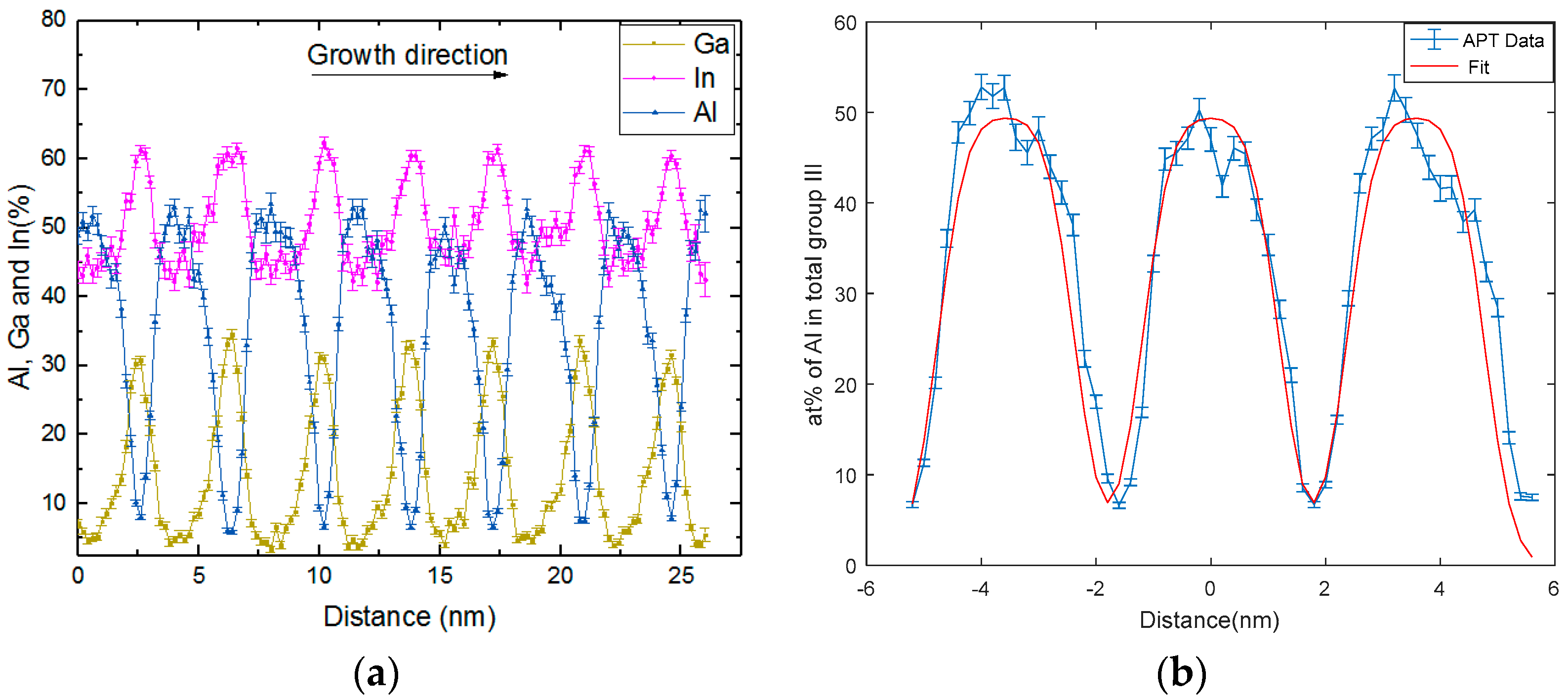
The individual layers in the thin-motif SL are about one-tenth the thicknesses of those in the thick-motif SL, and more importantly, closer to the typical thicknesses of the layers that comprise QCL designs. Figure 5 presents proxigram concentration profiles for the group III elements obtained from this sample. The concentration profiles immediately suggest that there is intermixing throughout the SL structure to produce quaternary alloy layers with compositions that vary continuously in the growth direction. None of the component layers appeared to be ternary, as they were intended to be.
Specifically, the concentration profiles suggest that the (InGa)As wells contained a minimum of 11 at. % Al on the group III site, and the (InAl)As barriers contain at least 4 at. % Ga on the group III site. The presence of the fourth element in the intended ternary layers of the SL was confirmed by examining the mass spectrum from a thin slice of “material” from the center of the ternary layers, and finding significant peaks from the fourth element. Pantzas et al. have reported similar concentration profiles for a QCL that is lattice-matched to InP, based on the high-angle annular dark-field scanning transmission electron microscopy (HAADF-STEM) image [9].
The semi-infinite solution to Fick’s second law used above does not apply to the thin-motif SL profile because the adjacent diffusion fields overlap. To model the intermixing as a result of diffusional processes in this SL, a solution to Fick’s second law that describes one-dimensional diffusion of a component from an initial slab of material of fixed width, 2h, and uniform concentration, C0 was used, specifically [8]:
The concentrations at positions x, which would result from the summed diffusion from series of three such slabs of initial composition In0.505Al0.495As and thickness 2.4 nm spaced on 3.7 nm centers were fit to the Al concentration profile, and they are shown in Figure 5b. The SL period in the APT reconstruction is ~10% smaller than that deduced from the HRXRD, given that a ±2.5% uncertainty is observed in the HRXRD fit for this SL.
The resulting diffusion distance was 0.56 ± 0.01 nm for the best fit at the 95% confidence interval. Assuming that the profile was obtained from approximately the middle of the SL—and it is only known that it was not from the bottom—a time at a temperature of 2800 s (half the total growth time) was applied, yielding an interdiffusion coefficient of 3.4 × 10⁻²³ m2s−1. This was calculated accounting for the 10% thicker SL period (as observed by HRXRD), and is in good agreement with that deduced for the thick-motif sample
The observed compositional grading at the interface could either result from; (a) surface segregation at the growth front during the layer growth or growth pause between SL layers [10,11], and/or (b) solid-state diffusion during the growth of subsequent layers, due to continued annealing as the structure is grown. Based on the growth rates in Table 1, the growth of 40 stages within a typical QCL active region takes ~6.42 hr (including the 5 s pause time in between each layer) [12]. Using the diffusivity determined for the thin-motif SL results in a diffusion distance of 1.8 nm for the first layer within the first stage of the active region, while the first layer in the 40th stage would exhibit a diffusion distance of 0.3 nm if diffusion were responsible for the intermixing. This rather large discrepancy in interfacial grading between the first and the last stage of a QCL would be expected to have a significant impact on device performance, since the QCL designs are quite sensitive to SL layer thickness and composition.
However, according to the estimated diffusivity versus temperature profile for an InGaAs/InAlAs heterostructure grown by MBE and having undergone lamp annealing [13], D is projected to be in the 10−22 m2s−1 range, which in turn indicates that solid state diffusion cannot be ruled out as a possible mechanism for observed composition profiles. From HRTEM analysis on similar QCL structures, the differences in layer thicknesses from the first to the last stage are seen to be within the measurement error. Additional APT experiments are required to analyze the interfaces in the first and the last stages of a QCL, to ascertain which mechanism or combination of mechanisms result in the observed composition gradients.
Figure 5 suggests some degree of asymmetry in the interfacial composition profile, which is not accounted for in the fitting. The veracity of the asymmetry could be tested by running the atom probe experiments from the substrate down, in the opposite direction to that used in this study, but such experiments have not yet been achieved. Asymmetric graded interfaces (2.5–4.5 nm in width) have also been observed for lattice-matched InAlAs/InGaAs SL structures grown by OMVPE [2], and for InGaAsP multiple quantum well (MQW) structures where Ga and As are diffused asymmetrically into the lower and upper InP buffer layers [14], as well as for InGaN/GaN quantum wells where the upper InGaN/GaN interface is found to be 1.3 nm wide and the lower interface is 0.6 nm wide, in that study [15]. Lattice-matched InAlAs/InGaAs QCL active regions grown by molecular beam epitaxy (MBE) also exhibit four monolayers of compositional grading in the interfaces [10]. Indium segregation was not indicated at any interfaces in either of the SLs studied here, unlike what was reported in Ref [2].
5. Conclusions
Two InxAl1−xAs/InyGa1−yAs SL structures with different compositions, layer thicknesses, and strains grown on InP substrates were analyzed by APT. Fitting the compositional profile to solutions to Fick’s second law of diffusion provided an estimate for the diffusion length in the range of 0.54–0.56 nm. The interdiffusion coefficient for both structures is in the range of 3–4 × 10⁻²³ m2 s−1, which is within acceptable agreement with that reported for similar materials. The observed intermixing could be due to surface segregation or bulk phase diffusion, or a combination. When the SL layers’ thicknesses are on the order of a typical QCL structure, the intended ternary layers are found to be quaternary alloys. Future work will include APT of the QCL, the implementation of designs for the same accounting for the interface grading, and study of the effects of growth parameters on the intermixing.
Author Contributions
Conceptualization, A.R., W.C., J.D.K., S.E.B., T.F.K., T.E. and L.J.M.; Formal analysis, A.R., W.C., J.D.K., S.E.B., T.F.K., T.E. and L.J.M.; Investigation, A.R., W.C., J.D.K., S.E.B., T.F.K., T.E. and L.J.M.; Methodology, A.R., W.C., J.D.K., S.E.B., T.F.K., T.E. and L.J.M.; Project administration, S.E.B., T.F.K., T.E. and L.J.M.
Funding
This work is supported by The National Science Foundation, Materials Research and Engineering Center (DMR-1121288) and Partners for Innovation (PFI) 1317292, and Navy STTR N68335-11-C-0432 and Air Force Research Laboratory FA8650-13-2-616
Conflicts of Interest
The authors declare no conflict of interest.
References
- Botez, D.; Kirch, J.D.; Chang, C.; Boyle, C.; Kim, H.; Oresick, K.M.; Sigler, C.; Mawst, L.J.; Jo, M.; Shin, J.C.; et al. High internal differential efficiency mid-infrared quantum cascade lasers. Proc. SPIE 2017, 10123, 101230Q. [Google Scholar]
- Wang, C.A.; Schwarz, B.; Siriani, D.F.; Connors, M.K.; Missaggia, L.J.; Calawa, D.R.; McNulty, D.; Akey, A.; Zheng, M.C.; Donnelly, J.P.; et al. Sensitivity of heterointerfaces on emission wavelength of quantum cascade lasers. J. Cryst. Growth 2017, 464, 215–220. [Google Scholar] [CrossRef]
- Wood, A.W.; Guan, Y.; Forghani, K.; Anand, A.; Kuech, T.F.; Babcock, S.E. Unexpected bismuth concentration profiles in metal-organic vapor phase epitaxy-grown Ga(As1−xBix)/GaAs superlattices revealed by Z-contrast scanning transmission electron microscopy imaging. APL Mater. 2015, 3, 036108. [Google Scholar] [CrossRef]
- Rajeev, A.; Mawst, L.J.; Kirch, J.D.; Botez, D.; Miao, J.; Buelow, P.; Kuech, T.F.; Li, X.; Sigler, C.; Babcock, S.E.; et al. Regrowth of quantum cascade laser active regions on metamorphic buffer layers. J. Cryst. Growth 2016, 452, 268–271. [Google Scholar] [CrossRef]
- Gault, B.; Moody, M.P.; Cairney, J.M.; Ringer, S.P. Atom Probe Microscopy; Springer: New York, NY, USA, 2012. [Google Scholar]
- CAMECA IVAS. Available online: http://www.cameca.com/service/software/ivas (accessed on 1 August 2018).
- Vurpillot, F.; da Costa, G.; Menand, A.; Blavette, D. Structural analyses in three-dimensional atom probe: A Fourier transform approach. J. Microsc. 2001, 203, 295–302. [Google Scholar] [CrossRef] [PubMed]
- Crank, J. The Mathematics of Diffusion, 2nd ed.; Oxford University Press: Bristol, UK, 1975. [Google Scholar]
- Pantzas, K.; Beaudoin, G.; Patriarche, G.; Largeau, L.; Mauguin, O.; Pegolotti, G.; Vasanelli, A.; Calvar, A.; Amanti, M.; Sirtori, C.; et al. Sub-nanometrically resolved chemical mappings of quantum-cascade laser active regions. Semicond. Sci. Technol. 2016, 31, 055017. [Google Scholar] [CrossRef]
- Offermans, P.; Koenraad, P.M.; Wolter, J.H.; Beck, M.; Aellen, T.; Faist, J. Digital alloy interface grading of an InAlAs/InGaAs quantum cascade laser structure studied by cross-sectional scanning tunneling microscopy. Appl. Phys. Lett. 2003, 83, 4131–4133. [Google Scholar] [CrossRef] [Green Version]
- Marmalyuk, A.A.; Govorkov, O.I.; Petrovsky, A.V.; Nikitin, D.B.; Padalitsa, A.A.; Bulaev, P.V.; Budkin, I.V.; Zalevsky, I.D. Investigation of indium segregation in InGaAs/(Al)GaAs quantum wells grown by MOCVD. 2002, 237–239, 264–268. [Google Scholar] [CrossRef]
- Botez, D.; Kirch, J.D.; Boyle, C.; Oresick, K.M.; Sigler, C.; Kim, H.; Knipfer, B.B.; Ryu, J.H.; Lindberg, D., III; Earles, T.; et al. High-efficiency, high-power mid-infrared quantum cascade lasers. Opt. Mater. Express 2018, 8, 1378–1398. [Google Scholar] [CrossRef]
- Seo, K.S.; Bhattacharya, P.K.; Kothiyal, G.P.; Hong, S. Interdiffusion and wavelength modification in In0.53Ga0.47As/In0.52Al0.48As quantum wells by lamp annealing. Appl. Phys. Lett. 1986, 49, 966–968. [Google Scholar] [CrossRef]
- Megalini, L.; Bonef, B.; Cabinian, B.C.; Zhao, H.; Taylor, A.; Speck, J.S.; Bowers, J.E.; Klamkin, J. 1550-nm InGaAsP multi-quantum-well structures selectively grown on v-groove-patterned SOI substrates. Appl. Phys. Lett. 2017, 111, 032105. [Google Scholar] [CrossRef]
- Liu, F.; Huang, L.; Davis, R.F.; Porter, L.M.; Schreiber, D.K.; Kuchibatla, S.V.N.; Shutthanandan, V.; Thevuthasan, S.; Preble, E.A.; Paskova, T.; et al. Composition and interface analysis of InGaN/GaN multiquantum-wells on GaN substrates using atom probe tomography. J. Vac. Sci. Technol. B 2014, 32, 051209. [Google Scholar] [CrossRef]
Figure 1.
Schematic diagrams of the motif characteristics of the superlattice samples.

Figure 2.
High-resolution X-ray diffraction (HRXRD) (004) ω-2θ scan for the thick-motif SL with simulations: (red) abrupt SL interfaces and (black) SL with a 1 nm thick constant composition intermixing layer. All scans are offset vertically for clarity.
Figure 2.
High-resolution X-ray diffraction (HRXRD) (004) ω-2θ scan for the thick-motif SL with simulations: (red) abrupt SL interfaces and (black) SL with a 1 nm thick constant composition intermixing layer. All scans are offset vertically for clarity.

Figure 3.
Atom maps for the obtained atom probe tomography (APT) for (a) thick-motif SL (b) thin-motif SL.
Figure 3.
Atom maps for the obtained atom probe tomography (APT) for (a) thick-motif SL (b) thin-motif SL.

Figure 4.
(a) Proxigram concentration profiles for the group III elements perpendicular to the interface in the thick-motif SL. Error bars represent the count of the statistical precision of the atom probe data; (b) Measured Al concentration profile, together with a best-fit semi-infinite solid solution to Fick’s second law of diffusion applied to the InGaAs–InAlAs interface.

Figure 5.
(a): Proxigram for thin-motif SL showing only group III concentrations. (b) Diffusion length estimation by fitting Fick’s law of diffusion to the Al content profile.
Figure 5.
(a): Proxigram for thin-motif SL showing only group III concentrations. (b) Diffusion length estimation by fitting Fick’s law of diffusion to the Al content profile.


Table 1.
Growth rates measured in calibration runs for III:V precursor ratios used to grow each superlattice (SL).
Table 1.
Growth rates measured in calibration runs for III:V precursor ratios used to grow each superlattice (SL).
| Material | V:III Precursor Ratio | Growth Rate (nm/s) |
|---|---|---|
| Thick-motif SL | ||
| In0.37Al0.63As | 428 | 0.10 |
| In0.67Ga0.33As | 315 | 0.14 |
| Thin-motif SL | ||
| In0.44Al0.56As | 375 | 0.12 |
| In0.60Ga0.40As | 387 | 0.11 |
Table 2.
SL layer compositions and SL periods as obtained by HRXRD simulations and APT reconstructions.
Table 2.
SL layer compositions and SL periods as obtained by HRXRD simulations and APT reconstructions.
| HRXRD Composition; Period | APT Composition; Period | |
|---|---|---|
| Thick-motif SL | In0.37Al0.63As/In0.67Ga0.33As; 43.5 nm | In0.38Al0.62As/In0.69Ga0.31As; 38.6 nm |
| Thin-motif SL | In0.44Al0.56As/In0.60Ga0.40As; 4.1 nm | In0.46Al0.50Ga0.04As/In0.58Ga0.31Al0.11As; 3.7 nm |
Table 3.
Diffusion lengths obtained by fitting Fick’s second law to Al and Ga concentration profiles in the thick-motif sample (Table 2), not accounting for the 10% discrepancy between HRXRD and APT SL period measurements.
Table 3.
Diffusion lengths obtained by fitting Fick’s second law to Al and Ga concentration profiles in the thick-motif sample (Table 2), not accounting for the 10% discrepancy between HRXRD and APT SL period measurements.
| Interface | Diffusion Length (nm) for Al | Diffusion Length (nm) for Ga |
|---|---|---|
| InAlAs–InGaAs | 0.52 ± 0.02 | 0.54 ± 0.04 |
| InGaAs–InAlAs | 0.51 ± 0.02 | 0.58 ± 0.03 |
© 2018 by the authors. Licensee MDPI, Basel, Switzerland. This article is an open access article distributed under the terms and conditions of the Creative Commons Attribution (CC BY) license (http://creativecommons.org/licenses/by/4.0/).
Share and Cite
MDPI and ACS Style
Rajeev, A.; Chen, W.; Kirch, J.D.; Babcock, S.E.; Kuech, T.F.; Earles, T.; Mawst, L.J. Interfacial Mixing Analysis for Strained Layer Superlattices by Atom Probe Tomography. Crystals 2018, 8, 437. https://doi.org/10.3390/cryst8110437
AMA Style
Rajeev A, Chen W, Kirch JD, Babcock SE, Kuech TF, Earles T, Mawst LJ. Interfacial Mixing Analysis for Strained Layer Superlattices by Atom Probe Tomography. Crystals. 2018; 8(11):437. https://doi.org/10.3390/cryst8110437
Chicago/Turabian StyleRajeev, Ayushi, Weixin Chen, Jeremy D. Kirch, Susan E. Babcock, Thomas F. Kuech, Thomas Earles, and Luke J. Mawst. 2018. "Interfacial Mixing Analysis for Strained Layer Superlattices by Atom Probe Tomography" Crystals 8, no. 11: 437. https://doi.org/10.3390/cryst8110437
Note that from the first issue of 2016, this journal uses article numbers instead of page numbers. See further details here.