1. Introduction
Since 1990, photonic crystals (PhCs) have been identified to be a versatile method to modify the way optical photons travel through a medium. The periodical structuration of the dielectric constant was found to offer control over the electromagnetic waves allowed to travel in the material, whenever the periodicity was on the same scale of the wavelength.
The very first contribution to the underlying idea of PhCs was published by Yablonovitch [
1], who formulated the theoretical basis of a forbidden band gap created by using a Fabry–Perot three-dimensional resonator with periodicity
/2. Further studies led to an experimental probing of the photonic crystal band gap using microwaves [
2]. The band structure was recorded performing a scan over different angles of incidence and frequencies impinging on the sample, and a band gap of unallowed wave vectors was observed. This knowledge opened the way toward a wide number of applications in the years to come:
optical logic devices, using nonlinear effects that cause a dynamic shift in the location of the band gap. It was demonstrated first by Scalora in 1994 that this non-linear mechanism can induce intensity-dependent pulse transmission and reflection (optical switching, ON/OFF), together with pulse shape modulation [
3]. This information can be used to build Boolean functions and perform logical operations.
Sensors and biosensors that make use of shifts of the PhC micro-cavity resonant frequency [
4].
Photonic crystal fibers. Many unique properties are associated with a structured fiber, such as single-mode operations over a wide wavelength range [
5] and over a very large mode area [
6].
Laser application; again micro-cavities, but filled with laser active material [
7].
Photonic crystal lasers for a single-photon source [
8].
Efficient photovoltaic devices with one-dimensional and two-dimensional photonic crystal patterns [
9].
Photonic crystal waveguides [
10] and nanophotonic circuits [
11].
Light extraction from LEDs [
12] and inorganic scintillators, making use of a PhC slab as a diffraction grating.
This review will focus on the last application listed and more specifically on how PhC slabs can be applied to inorganic scintillators to improve energy and time resolution.
PhC slabs are defined as thin layers with 1D, 2D or 3D periodicity of the dielectric constant, which can increase the light extraction efficiency from high refractive index media. Joannopoulus first showed in 1997 how this principle could be applied to LEDs, and the method was considered a valuable and more efficient alternative to texturing the readout face. Following this work, Borodinsky [
13] gave the experimental confirmation of an extraction efficiency enhancement up to a factor of four, using a triangular pattern of holes coupled to a glass substrate. The PhC slab was found to both enhance spontaneous emission through the Purcell effect and increasing the extraction efficiency of emitted photons, otherwise trapped due to total internal reflection (TIR).
The Crystal Clear group [
14] at CERN was the first to explore the possibility to use the same technology applied to inorganic scintillators, knowing that the presence of a critical angle due to high refractive index crystals was similar to the problem encountered with LEDs. First with Kronberger [
15], followed by Knapitsch [
16,
17,
18], an experimental method was developed to obtain the best photonic crystal slab for each application. Several other groups started to put efforts toward the same field, and many collaborations started to grow with the common objective of increasing the light output of high refractive index crystals. In the following sections, we will explain in detail the theory, simulation tools and results obtained, summarizing what has been accomplished for those approaching the field for the first time, as well as the questions that remain open.
2. Inorganic Scintillators: State-of-the-Art
2.1. Design Specifications for Different Applications
Today, inorganic scintillators are widely used in various applications based on the detection of ionizing radiation such as high energy physics, medical imaging, homeland security, material research, thermal neutron detection and others.
The characteristic parameters of inorganic scintillators are density, light yield, energy resolution, rise time and decay time, emission wavelength, radiation hardness and production costs. The choice of these parameters depends on the requirements that different applications have with regard to one or many of them. Since a perfect scintillator matching all requirements does not exist, a trade-off between various parameters has in general to be found to best match the needs of such applications.
For high energy physics, scintillators are used to detect high energy particles (up to a few hundred GeV) in a generally harsh radiation environment, leading to severe constraints in terms of stopping power and radiation hardness. Scintillators for future particle physics experiments are in addition required to have a good time resolution to improve the detection probability of rare events through pile up suppression. Furthermore, high energy physics experiments in general have large detection volumes, leading to additional constraints in terms of the cost-effective production of large volumes in a reasonable amount of time.
On the other side, for positron emission tomography (PET) applications, the key performance parameters are the quality of the reconstructed image together with the possibility to detect small tumors and to access dynamically-different molecular pathways with the minimum radioactive dose injected to the patient. The main requirements for scintillators are thus to have a high sensitivity and a high spatial, energy and time resolution. High sensitivity is achieved through a high stopping power and high spatial resolution through crystal size. A good energy resolution enabling an efficient rejection of Compton and scattering events is achieved through a high light yield. A good time resolution is achieved through a high light yield and a very short rise and decay time for the scintillation light. A proper choice of these parameters allows for a significant dead time reduction and a much better coincidence time resolution, leading to an improved image quality and thus to a reduced dose delivered to the patient and a shortened duration of the exam.
In homeland security applications, scintillators are used to detect the presence of explosives and illicit nuclear material and, if possible, to identify their exact composition. A good energy resolution is thus required to identify the characteristic energies of the detected radiation and to precisely identify the radioisotopes present in the object under investigation. The capability to efficiently discriminate between neutrons and gammas also becomes an important feature of the detecting device.
In thermal neutron applications, scintillators are used to build diffractometers. Spallation neutron sources are expensive to build and to operate, and the hadronic interaction exploited by neutron diffraction instruments is inherently weak. The resulting strong requirements on detection efficiency and signal-to-noise ratio impose therefore the use of scintillators with the highest possible light output.
The performance of scintillators in terms of light yield, energy and time resolution is, however, intrinsically limited by fundamental physical effects as explained below, and such limitations can have a decisive impact on the choice of suitable scintillator materials.
2.2. Limits on Light Yield
The signal-to-noise ratio is an important parameter in all radiation detection devices using scintillators. While the noise remains constant, the strength of the signal depends on the number of photoelectrons generated in the photodetector used to readout the scintillator and is proportional to the light yield (), defined as the number of scintillation photons generated per unit of energy deposited by the incoming particle, collected in the photo-cathode and that can be converted into photoelectrons.
This depends on the number of photons produced in the crystal by the incoming particle interaction and the light collection efficiency , which is a measure of all kinds of light losses along its way to the photodetector, such as reflection, absorption and diffusion in the crystal competing with extraction at the exit surface of the crystal.
is determined by the overall conversion efficiency of the energy of the incident particle (gamma or X-ray) to light emission (UV or visible) and given by the following formula:
with
the energy of incident particle,
the band gap energy,
S the transfer efficiency from ionization to the luminescence center and
Q the efficiency of luminescence [
19].
is a parameter varying from 2–3 for a wide range of scintillators [
20].
The light collection efficiency
depends on the optical properties of the crystal. The generally high refractive index of the scintillators and the consequently small critical angle will lower this efficiency. Several studies ([
21,
22,
23]) demonstrated also that the surface state, the edge quality and the type of wrapping used for the crystal play an important role in the efficiency of light collection
.
The light yield of the crystal can therefore be expressed by the following equation:
showing that the light yield is governed by the band gap energy, the transfer efficiency from ionization to luminescence and light collection efficiency. The Q factor is usually a constant close to one. It was shown that the optimal energy band gap to obtain high light yield materials varies with the type of activator [
24].
Maximizing the light yield not only requires selecting materials with an optimal band gap energy, but also optimizing the transport of the light such that the maximum photons reach the photodetector.
2.3. Limits on Energy Resolution
The factors impacting the energy resolution of a scintillator-based detector system are in general classified into three different categories:
Statistical fluctuations in the generation of scintillation photons and the conversion in photoelectrons in the photodetector, expressed by ;
Inhomogeneity in the bulk material (impurities, scattering centers) and the surface of the crystal (polishing, wrapping) leading to fluctuations of the amount of light transported to the photodetector, expressed by ;
Non-linearity of the scintillation photon yield as a function of the energy deposited by the incoming particle, due to statistical fluctuations of the ionization process and a non-uniform ionization density, expressed by .
Statistical fluctuations in the generation and detection of scintillation photons can be minimized by maximizing the light yield. The impact of inhomogeneity in the bulk and at the surface of the scintillator can be minimized by improving the purity of the raw material, controlling the crystal growth process parameters, optimizing the surface treatment and choosing appropriate reflector materials. Contributions from the non-linearity in the scintillation photon yield are more challenging to optimize and therefore constitute the main limitation for the optimization of the energy resolution. Extensive R&D has been carried out in the past by several groups [
25] to better understand these contributions.
2.4. Limits on Time Resolution
The intensity of the scintillation light as a function of time is in general described using a bi-exponential expression:
with
and
being the scintillation rise time and the scintillation decay time, respectively.
In the case of several different luminescence centers, Expression (
3) becomes a sum of exponentials. The decay time of a scintillator is related to the depopulation rate of the excited state: it is the result of radiative (
) and non-radiative (
) processes. For electrical dipole emission, the radiative process rate is inversely proportional to the oscillator strength
f, with a coefficient depending on the coordination of the emitting ions in the crystal lattice. It is typically expressed as:
with
the emission wavelength and nthe refractive index [
19]. Therefore, a shorter emission wavelength and a higher index of refraction favor a shorter decay time.
The time resolution of a scintillator-based detection system is a measure for the precision of the time stamp that can be attributed to the detection of a particle. The time resolution depends on the rate of photoelectrons above the detection threshold, which in turn depends on the time distribution of photons being converted in the photodetector. The main crystal parameters influencing the time resolution of a scintillator detector are the light yield and the rise and decay time of the scintillation process as illustrated by the following formula, derived by the Hyman theory:
The time resolution
can hence be improved by using scintillators with high light yield and short decay and rise time constants [
26,
27].
3. Rationale for Photonic Crystals
Increasing the extraction efficiency of the scintillation light from inorganic scintillators remains an important concern for improving the performance of scintillator-based ionization radiation detectors. Indeed, the goal for these detectors is to record the maximum information about the event at the origin of the ionizing radiation, and in particular:
If the spatial localization is generally achieved by the choice of a dense material and the combination of a number of individual detectors, finely segmented and distributed around the region of interest, the energy and time resolution are directly related to the amount of collected light.
The high Z materials used in these detectors, to ensure a high stopping power and a good localization for the ionizing radiation, generally have a high density of electrons and are characterized by a high index of refraction. For instance, LYSO:Ce (
), the most widely used crystal in the PET system, has an index of refraction of 1.82. This limits by the total internal reflection the amount of light collected by the photodetector, as the coupling material to the photodetector is usually an optical grease or glue with an index of refraction no higher than 1.5. As a consequence, the performance of the scintillator can be severely affected by the transit of the photons from the interaction point to the photodetector, where they will be converted into an electronic signal, leading to delays and absorption losses. For crystals with high aspect ratios, as the ones used in PET scanners, up to 50% of the scintillation light will not be collected [
28], even if Teflon wrapping and optical coupling are used, and a large fraction of the collected photons will be delayed by multiple bouncings in the crystal. Several years ago, we proposed to use photonic crystal slabs (PhC slabs), defined as thin dielectric layers structured with a 2D or 3D periodic pattern, to increase this efficiency [
29]. A higher light output, combined with a reduction of the average path length of the photons in the crystal before their extraction, leads to a better energy and time resolution.
3.1. Increasing the Light Output
In the case of the light output, the parameter of interest is the number of photoelectrons
registered after a particle has deposited its energy in the scintillator. Typically,
is expressed as:
, where
is the effective quantum efficiency of the photodetector:
. As already introduced in
Section 2.2,
is the light collection efficiency of the scintillation detector and summarizes the impact of all processes leading to losses during the transport of the scintillation photons from the production point to the active region of the photodetector. This includes absorption and scattering in the crystal bulk, absorption and diffusion at wrapping materials and reflection losses due to the mismatch of the refractive index of the scintillator, optical coupling and photodetector. These losses increase the statistical fluctuations of the light output and impact therefore the energy and time resolution. The use of PhC slabs can significantly improve this last point, as shown in this review.
3.2. Improving the Energy Resolution
A good energy resolution is a prerequisite for spectroscopic measurements and of particular interest for environmental conditions’ analysis, as well as for homeland security and non-proliferation control. For medical imaging applications (PET and single-photon emission computed tomography (SPECT)), a better energy resolution allows a higher rejection of tissue-scattered events and Compton events in the crystals and improves therefore the spatial resolution and the sensitivity. The sensitivity is a critical parameter of nuclear medical imaging, as it reflects the number of useful events per unit of injected dose to the patient. A higher sensitivity means a smaller injected dose or a better image contrast. A good energy resolution requires a good linearity of the scintillator response as a function of the energy released in the detector, as well as the highest possible light yield. The energy resolution is indeed statistically determined by the number of photoelectrons produced in the photodetector, which is directly proportional to the number of photons extracted from the crystal. Therefore, a high light yield will improve this statistical factor as: .
3.3. Improving the Time Resolution
In recent years, fast timing has emerged as a new requirement for scintillator-based detectors, generally related to the study of ultrafast phenomena, as well as to time-of-flight imaging techniques. It is mainly driven by high energy physics (HEP) to cope with higher event rates while minimizing pile-up, as well as by time-of-flight positron emission tomography (TOF-PET) applications to improve the image signal-to-noise ratio, with the potential to reduce the doses injected to the patients. Time resolutions in the 10-ps range are required in both cases, which boosts the research for scintillators with a high light yield and maximum collection efficiency of the scintillation photons.
The time resolution of a scintillator-based detector is directly driven by the density of photoelectrons generated in the photodetector at the leading edge of the signal. Increasing the light output and as a consequence the rate of photoelectrons produced in the photodetector at the early stage of the signal generation has a direct impact on the time resolution as previously illustrated by Relation (
5).
The scintillator rise time (
) plays a determinant role for the time resolution and requires a detailed analysis. It affects the photoelectron density in the early stage of the signal, which carries the ultimate timing information [
30]. As we have shown in a previous paper [
27], several factors contribute to the rise time of the signal produced by a scintillator. Among them, the light transport from the emission point in the crystal to the photodetector plays a significant role if we are aiming at time resolutions in the 100-ps FWHM range or better [
31]. Properly-designed photonic crystals allow a redistribution of the scintillation photons to the fast propagation modes in the crystal, further improving the time resolution.
3.4. Optimizing the Collimation of the Extracted Light
Other losses, such as Fresnel reflection, arise because of the nature of the optical interface between the crystal and the photodetector. This is stronger for higher impinging angles, where many effects might take place: lateral light losses in the coupling medium, at the photodetector windows and in the protective layers; less efficient and less prompt light detection in the photodetector for the photons absorbed too far from the amplification region; cross-talk between different detection pixels. Properly-designed photonic crystals can favor some light extraction modes and have the potential to collimate the light in certain directions. This property can be particularly useful if the different components of the light produced by a multi-functional meta-material at different wavelengths have to be readout separately [
32].
Figure 1 shows the measured angular distribution of three photonic crystal patches deposited on an LSO (
) crystal. Although these photonic crystals have been designed for increasing the light extraction efficiency and not optimized for a better collimation, the collimation effect is clearly visible. This effect can be exploited to further improve the performance of scintillator-based detectors. For instance, the application of specifically-designed photonic crystals to the lateral faces of the crystal could allow redirecting the light impinging at a large angle in the forward direction.
4. Theory of Photonic Crystal Slabs
As already mentioned, PhCs are nano- or micro-structured materials with a periodic dielectric function over at least one dimension. The properties of an electromagnetic (EM) wave traveling through the PhC can be modified by the presence of this periodicity, if certain conditions are matched. In the first part of this section, the theoretical framework needed to understand these conditions will be introduced, together with a detailed explanation about why PhC slabs can increase the number of scintillation photons extracted from a crystal. The discussion will then move on to the different kinds of PhC slabs available.
4.1. Basic Principles of Photonic Crystals: Towards Diffraction
A description of the effects produced by a PhC can be obtained by treating it as a simple diffraction grating. Whenever the periodicity is higher than half the wavelength, EM waves traveling across a periodic arrangement of (thin) dielectric material will be split over different diffraction orders. Diffraction intensities over the different orders can be evaluated by considering a field passing through a volume
V made of a periodic distribution of scattering centers. The higher the density of electrons inside these centers, the higher the number of dipoles that oscillate under the influence of the EM field. This causes the field to bend, resulting in a different propagation direction. The formula describing the amplitude of this phenomenon-caused by a certain scattering volume
V is [
33]:
which is a function of the phase shift
, the electron density
and the distance
r between the origin of an arbitrary coordinate system and the scattering center
. It can be demonstrated that this integral is non-negligible only for
, with the G reciprocal lattice vector of the system. All the photons passing through this PhC will have a modified k-vector direction and will therefore exit the interface with an angle dependent on the periodicity of the system and the diffraction order
m. This conclusion comes out naturally from a more rigorous explanation, which starts with the equation identifying the standing wave allowed to propagate inside a PhC:
which is a reformulation of Maxwell equations called the master equation.
is the frequency of the incident field;
c is the speed of light; and
the dielectric constant of the PhC material. For a detailed explanation about how to derive it, refer to [
10,
33]. This eigen-value problem can be solved for a specific structure
, which defines the theta operator (
), in order to obtain the modes available
H. We can then insert
H into:
to obtain
E [
10] and have a complete description of the eigen-modes available in our system. These modes provide us with everything we need to know about the PhC, and the following will give an example about what we can do with this information.
4.2. Bloch Modes and Equi-Frequency Diagram
Consider a simple 2D grating of pillars placed in a square lattice, surrounded by air, as the one depicted in
Figure 2. The symmetries of the system are the key to understanding most of the PhC slabs’ properties. Our system shows two main symmetries: discrete translational symmetry over x and over y for discrete steps of
and
, with
l an integer number. Whenever a symmetry is found for the system, its operator commutes with the theta operator of the master equation, and this means that they share a common eigen-space: each simultaneous eigen-function of the symmetry operators is therefore an eigen-function of the theta operator. Solutions of the master equation using the translation operator are much easier to find than for the theta operator in Equation (
7). These solutions are standing waves known as Bloch modes:
A Bloch state is an EM field inside the structures coherently scattering with itself. Because of the periodic form of Equation (
9), Bloch modes with
have the same eigen-value for Equation (
7). These modes form a degenerate set of the system, which is the key factor for the diffraction orders to rise. The eigen-functions of this degenerate set correspond to the same state, with the same eigen-value and same frequency, and photons impinging on the PhC slab with an allowed
can couple to any of the other
.
This periodicity implies also that we can confine our mode analysis to only the so-called irreducible Brillouin zone, since we expect periodic solutions for the rest of the pattern area. We can describe the irreducible Brillouin zone as the smallest possible area over which solutions of the master equation are not redundant. We introduce here the concept of reciprocal space: a vector with component
becomes a reciprocal vector with components
and
:
For a square lattice, the new coordinates will be
and
. We can cover the entire reciprocal space repeating the irreducible Brillouin zone, mirroring and translating it.
Figure 3 shows the irreducible Brillouin zone for the simple geometry of
Figure 2. To simplify the situation even more, one could define a certain path of the
vector over the irreducible Brillouin zone. It is a widely-used technique to follow the border of the irreducible Brillouin zone starting with a
, following to M and then X, as indicated by the arrows in the picture. This method allows one to show much information using just one two-dimensional graph, similar to the one shown in
Figure 4, called a band diagram. This amount of information is unfortunately not enough if working with a wavelength smaller than the periodicity, which is our field of application. In this case, an analysis extended to the region as big as the wave-vector of the incoming radiation is needed and spans over all the possible
combinations. In the case of PhC slabs there is no periodicity over
. We will therefore consider an iso-frequency diagram, or equi-frequency contour (EFC), as the one shown in
Figure 5. This plot shows one single mode as a color map of the allowed
in the
plane.
and
are the components of the k-vector of the incident photon for which the symmetries explained at the beginning of the section apply. As already said, we can couple to any of the degenerate modes that have
, with
and
, so we will need to extend the region of interest to a few more reciprocal lattice points. An example of the area needed superimposed with the so-called Ewald construction is shown in
Figure 6. The periodicity of the first mode is clearly visible over
and
.
Each photon with defined direction and frequency may intercept one of these standing waves, being then able to couple to the modes of the degenerate set with a certain probability. These probabilities have a non-trivial evaluation, and simulation tools are needed to calculate them, as we will explain in the next section. Once the photon interacts with the PhC slab, the extraction parameters will be modified from the one expected using Snell’s law. Consider a k-vector version of Snell’s law (
Figure 7):
This can be reinterpreted as a
conservation rule:
. The following notation is used:
and
; the subscript
will always indicate the vector component parallel to the interface. It is now possible to introduce the effect of the degenerate set
. Depending on the mode number, photons will be bent to an angle dependent on the initial properties of the incoming photons and the PhC slab parameters:
where we have assumed
for air as the surrounding medium. This last equation is named after the physicist Von Laue, who first introduced the idea of wave vector coupling dependent on the reciprocal lattice point (Laue condition).
The length of the k-vector has to be constant for energy conservation. This is simply understood taking into account that the frequency of the dipole emission generated by the electrons should match the incident frequency. An additional formula is then required to redefine the component perpendicular to the surface:
where
is the refractive index of the substrate on which the PhC slab is applied and
the external medium. Notice that for negative values of m in the equation, photons with an angle bigger than the critical angle can be transmitted in the outside medium. This is the feature of PhC slabs that one would need to exploit in order to increase the extraction efficiency of inorganic scintillators. To visualize such an effect, a simple experiment was set up:
Figure 8 shows the diffraction orders for a green laser impinging normal to an LYSO inorganic scintillator; the laser beam enters the flat, polished, back surface and reaches the front face where a PhC slab is imprinted. The main diffraction angle is shown in purple, while secondary orders coming from other symmetries of the system are shown in blue and red. Above the critical angle, half of these orders are still extracted from the scintillator.
4.3. Conical Structure: A Different Approach
Another method that can be used when trying to efficiently extract light from a high refractive index (RI) medium is to apply an anti-reflective coating. The purpose is to reduce Fresnel reflection under the critical angle, which can be achieved using sub-wavelength periodicity,
, and high aspect ratio structures [
34]. Unfortunately, working with periodicity smaller than the wavelength results in no degenerate states available inside the air circle (
Figure 6), and this means that only the zeroth order will be transmitted outside the crystal: no diffraction will occur, and this can strongly limit the potential gain in light extraction. One possible way is to use conical PhC slabs in a regime of
, with P period of the pattern, where diffraction still can take place, but also anti-reflection features show up. This particular topic will be treated in more detail in the Results
Section 8.
4.4. Importance of the Refractive Index of PhC Slabs
Equation (
6) shows the dependency of the amplitude on the electronic density. To fully exploit the diffraction behavior of PhC slabs, this amplitude has to be as high as possible, and besides the angular dependency (phase shift), this is dominated by the electron density. Materials that match this requirement are the ones with high RI. The formula describing the refractive index (
n) is:
which shows a direct correlation between the RI and
, that is the density of electrons within a unit volume and with natural frequency
.
is the damping factor;
and
m are respectively the charge and the mass of the electron; and
is the frequency of the incoming EM field. Being able to use high RI materials for PhC slabs will then lead to stronger scattering amplitudes and therefore brighter diffraction orders.
Regarding the
, when an EM wave of the form
travels through a non-patterned slab with damping factor
and thickness
, the formula describing the field transmitted is:
where we have considered the RI to have the simplified form
, with real and imaginary independent components. The term C is the
, modulated by a term B that just changes the phase of the wave. The term A describes a decrease in the amplitude of the field and increases with
and the damping factor
, which is now hidden inside the
.
This imaginary part of the index of refraction should be included in the simulations whenever absorbing materials are used to create PhC slabs. A widely-used instrument to measure the is the ellipsometer, and it has to be used in the case of non-perfectly transmitting materials.
5. Simulations
Different simulation tools are used to perform mode analysis of the structures (MPB), visualization of EM fields and diffraction orders’ propagation directions (COMSOL), calculation of transmission efficiencies (CAMFR) and finally ray trace optical photons in the substrate, the PhC slab and the surrounding setup (Geant4). This section will introduce these software programs, giving brief insight into how they work and explaining why they are useful in the PhC slab prototyping.
Some of these packages are freely available, and references are provided.
5.1. Cavity Modeling Framework
The cavity modeling framework (CAMFR, [
35]) is a rigorous coupled-wave analysis tool (RCWA) that was developed by Peter Bienstmann during his PhD. It has a Python interface; therefore, it is easy to use and to modify, being a user-friendly programming language. It implements C, C++ and Fortran libraries to calculate EM field expansion: these libraries are fast and reliable and still are transparent to the user thanks to Python ‘wrap’ function.
The code is a frequency domain eigen-value solver, which solves the master equation (Equation (
7)) for source-free harmonic eigen-fields. The volume of the system is discretized in a layered stack, and inside each layer, the scattering matrix method is applied for a given frequency [
36] using the mode matching principle. This method was proven to be consistent with other finite-difference time domain (FDTD) methods [
37], but being orders of magnitude faster for a large variety of structures. Moreover, spurious effects of numerical dispersion arising in FDTD are not seen in CAMFR.
5.2. MIT Photonic Bands
MIT photonic bands (MPB, [
38]) is a free package released by MIT that computes full-vectorial 3D Bloch states, thus the eigen-states of the PhC slab. As CAMFR, it is a frequency domain software. The geometry is simulated in an finite element domain (FEM) layout, through the input interface for which the Scheme programming language is used. Having to simulate PhC slabs, which involves wave-guiding, this method is fast and reliable if compared to the standard FDTD method, which is based on time domain calculation: spurious effects of numerical dispersion arising in other techniques using FDTD are not seen with eigen-frequency expansion. MPB can be used to analyze the modes available in a certain dielectric, spanning over the entire irreducible Brillouin zone.
5.3. Geant4
Geant4 [
39] is an open-source Monte Carlo simulator toolkit with a particle physics background. The main fields of application include high energy, nuclear and accelerator physics, as well as studies in medical and space science. It has been widely extended over the years to match the requirements of the community and today constitutes one of the most complete codes of its kind. This code can be used for simulating gamma interactions, optical photon transport in the scintillator up to the intersection with the PhC slab and after the interaction with this surface, up to the photodetector. The steps that should be implemented while simulating the system are: the index of refraction of all the materials that could interact with the optical photons, as a function of the wavelength (crystal, surrounding medium, wrapping, optical coupling, photodetector); the crystal emission and absorption spectrum; the surface state of the crystal (
parameter and reflection type selection; see
Figure 9); the energy and direction of the incoming gamma rays, as well as the density of the scintillator (defines the stopping power); the reflectivity of the surrounding materials. Geant4 allows for an easy implementation of all these parameters. One drawback of using a Monte Carlo simulator is that optical photons are treated only as particles, and the program does not take into account photonic effects. See
Section 5.5 for more details.
5.4. Other Tools
Several other simulation tools exist. The purpose of this section is to give a quick overview of all of them and to provide useful references.
Tools that have been used to calculate PhC slab propagation and transmission:
COMSOL Multiphysics
® [
40], a flexible tool for simulating PhC slabs. The COMSOL package that can be used with the purpose of visualizing EM fields and diffraction effects is called the Wave Optics Module.
GD-Calc is another RCWA software, based on MATLAB. The propagation in the PhC slab is calculated using a scattering matrix method [
41].
Lumerical, a tool for both FDTD and eigen-mode expansion calculations [
42].
S4, Stanford University [
43]. Another frequency domain RCWA solver embedded in a LUA (scripting language) environment.
Tools that have been used to ray trace the particles inside the scintillator:
Litrani [
44], a general purpose Monte Carlo program used to simulate light propagation.
Zemax [
45], an optical design program based on ray tracing.
DETECT2000 [
46], a ray tracing program that exploits the functionality of computer-aided design (CAD) to model the geometry and materials of the system.
5.5. Combining Ray Tracing with RCWA Simulations
Once the scintillator is treated with PhC slabs, in order to simulate the complete system (crystal, PhC slab and photodetector), one would need to combine both ray tracing information and photonic behavior. Unfortunately, there is still no fast and efficient way yet to implement an optimization with a single tool that merges these properties together. A possibility is offered by a combination of the separate tools CAMFR and Geant4, which can be used to optimize some of the system parameters to maximize the light extraction and energy resolution of the detector.
The angular distribution of the first incidence photons is initially generated by Geant4: only the first time a photon impinges on the readout face is counted, since any other reflection will be affected by the presence of the PhC slab itself. The angular distribution is then used by CAMFR to optimize the pattern parameters, for instance the period (P) and diameter (D) of the structures, and for a combination of transverse electric (TE) and transverse magnetic (TM) transmitted modes. Once the pattern optimized for first incidence is determined, the transmission probability for each angle of incidence is given as an input to a Geant4 surface. The source code of Geant4 has to be modified to accept the output of CAMFR. Geant4 is now able to calculate the light yield (LY) gain for a given structure.
Below is a summary of the optimization steps required:
Simulation of the scintillator with a ray tracing program and calculation of the light angular distribution information. The number of gamma interactions to be used needs to be high enough to generate a good enough statistics to produce a smooth distribution.
Run the PhC simulation tool to obtain the transmission of the light as a function of the impinging angle of the plane wave. Provide the angular distribution and calculate the transmission. Loop the simulation over different parameters in order to find the configuration that gives the higher light extraction efficiency.
Once the optimized configuration is found, implement the new transmission of the PhC surface into the scintillator + photodetector system. Run again the ray tracing simulation tool, now counting all the photons that enter the photodetector window, which is the value that can be compared with
experimental data. A contour plot showing an optimization example of a photonic crystal pattern over a period and diameter is shown in
Figure 10.
6. PhC Slab Production Methods
The progress in patterning techniques has been pushed by the micro- and nano-electronics industry for decades. The first integrated circuit was printed in the 1960s using contact lithography. Afterwards, mostly optical projection lithography was developed due to its high throughput. Furthermore, electron beam lithography techniques have been developed to provide the high resolution masks needed for optical lithography [
48].
When the development of patterning techniques started, the patterns that could be produced were in the 10 µm scale. Nowadays, it is already possible to pattern structures smaller than 20 nm and with a high throughput [
48].
Even though most of the processes in the nano-electronics industry are well developed and have a high throughput, the processes generally need adjustments when being used for imprinting scintillators. This can be either to solve problems intrinsic to the patterning process, such as the need for a conducting layer on a scintillator to be able to imprint with electron beam lithography, or practical issues with the equipment, such as samples that are much too high for the equipment that is developed for imprinting only several millimeters of thin silicon wafers. However, in principle, the techniques can be used for the purpose of producing nano-patterns on inorganic scintillators.
Nowadays, nano-patterning techniques are being developed for many different applications, introducing also more novel techniques such as patterning with scanning probes or by using self-assembly techniques.
While investigating nano-patterning techniques for the improvement of light extraction efficiency , the physical properties of the material that is to be imprinted play an important role.
Since the interaction of the pattern with the scintillation light is based on the electric potential created by the PhC slab, the extraction can be improved mostly by using materials that create a high electric potential, meaning a material with an as high as possible RI, as is explained in
Section 4.4. Direct patterning of the scintillator itself is therefore usually not the best option, and preference is given to imprinting a so-called optical layer, consisting of a high RI material deposited on top of the scintillator. Examples of materials that can be used as high RI materials are
and
. Another approach could be to create a photonic crystal pattern in a low RI material, for instance by directly patterning the scintillator, and afterwards, depositing a high RI material on top of the structure, for instance by using atomic layer deposition (ALD), to increase the effective RI of the pattern. Also in this case,
and
are good candidates as high RI materials. An example of using ALD to increase the effective RI of a pattern produced with polystyrene nanospheres, a technique explained in
Section 6.4.1, is given in [
49,
50].
Another important characteristic is the optical transparency of the material. Since optical absorption of the material will decrease the amount of extracted light, it is preferred to use a material with a high optical transparency.
An important note that one should consider when reviewing the different patterning techniques is the process of transferring the pattern from a resist or hard mask to the final optical layer. If it is necessary to transfer the pattern to a different layer, the limits of the transfer of the chosen resist or hard mask for the final material have to be considered. This could be a limitation in resolution or in the maximum aspect ratio that can be obtained. However, discussing the subject in more detail is outside the scope of this review.
6.1. Scanning Beam Lithography
6.1.1. Electron Beam Lithography
Electron beam (e-beam) lithography is a patterning process where no mask is needed. The machine, first used in 1960, had originally been developed from scanning electron microscopy [
51]. The patterning is performed by exposing a layer of resist (deposited on top of the PhC slab material), which is an electron-sensitive medium in this case, with a focused electron beam. Depending on the chemicals used in the next step of the development, either the parts of the resist that are affected by the e-beam are washed or the parts that have not been exposed to the e-beam. Afterwards, the pattern is transferred to the final layer by using, for instance, reactive ion etching (RIE) [
51].
The fact that e-beam lithography does not need a mask makes it a versatile technique. Furthermore, the resolution of this method is extremely high. Unlike optical lithography (see
Section 6.2), in this case, the wavelength of the particles used for the pattering does not contribute significantly to the resolution. Depending on the resist and process parameters used, the accuracy can be higher than 10 nm [
48].
Unfortunately, e-beam lithography is a patterning technique that is intrinsically very slow, making it extremely time consuming and expensive to use. The electrons are scattered by the space charge effect, and this effect is increased at higher currents, meaning that lower currents and therefore longer exposure times are needed for high-resolution patterning. Furthermore, the resist can only be exposed at the part where the e-beam is focused at that moment, and there is only one beam that scans the surface. This further limits the writing speed. In industry, the e-beam is therefore mainly used to produce masks for other lithography processes, which are then used many times. Attempts have been made to improve the patterning speed, by for instance introducing ways to have patterning with multiple beams from a single electron source. However, no real working example has been produced [
48,
51,
52,
53]
As a result, the e-beam is a good technique to produce prototypes of photonic crystals on scintillators; however, it is not scalable to large surfaces. An example of photonic crystals produced with e-beam lithography is shown in
Figure 11.
6.1.2. Ion-Beam Lithography
Also originating from the idea of scanning electron microscopy, ion-beam lithography is quite comparable to e-beam lithography, but instead of a beam of electrons, a beam of ions is used.
The benefit of using ions is that the resolution is not limited by the space charge effect. Therefore, the resolution can be higher compared to patterning with the e-beam, and the exposure time can be shorter. Furthermore, the resists used in ion-beam lithography are more sensitive, hence further reducing the required exposure times [
54].
Ion-beams can also be used by directly patterning the desired layer of PhC slab, instead of using a resist. This means no additional steps and processes are necessary to obtain the pattern in the required layer [
55]. This direct way of carving away the material is called milling and has historically been the main method used in ion-beam lithography [
56].
Even though the exposure times in ion-beam lithography are lower compared to e-beam lithography for obtaining the same resolution, the patterning technique is still slow, therefore making it unsuitable for patterning large surfaces. Furthermore, the implantation of ions in the layer to be patterned can occur. Especially in the case of nanopatterns for improving light extraction, this can be a serious problem, since it can produce absorption in the material to be patterned [
52].
An example of photonic crystals produced by direct milling of the scintillator is shown in
Figure 12.
6.2. Optical Lithography
Optical lithography has been the main way to produce integrated circuits by the micro- and nano-electronics industry for decades. Therefore, it is well developed, in the sense of high resolution, but also high throughput.
6.2.1. Optical Projection Lithography
There are multiple techniques in optical lithography to perform the patterning. One of the basic principles is optical projection lithography. Here a mask, which is a copy of the final pattern, is used to project light of a certain wavelength on a photosensitive resist. After developing the resist, the pattern can again be transferred to the final layer through reactive ion etching.
Figure 13 illustrates this imprinting technique.
The resolution in optical lithography is mainly limited by the wavelength of the light and the numerical aperture of the system. Therefore, to increase the resolution, one tries to always go to shorter wavelengths and higher numerical apertures, while still maintaining a good depth of focus. Already in the 1990s, deep UV (DUV) patterning techniques were used in integrated circuit production, using wavelengths down to 193 nm. To be able to further increase the numerical aperture, immersion lithography has been developed, improving the resolution to about 40 nm. Very recently, techniques have been developed to use extreme UV (EUV) techniques, using a wavelength of 13.5 nm. With all the developments, it is nowadays possible to pattern structures with a resolution higher than 20 nm. The chemical development of the resist also has contributed to the continuous increase in resolution [
48,
52,
56,
58].
Since the image of the mask is projected on the resist, a larger surface can be patterned all at once. This makes the technique much faster than for instance e-beam lithography, which was discussed in the previous
Section 6.1.1. However, the production of the mask is expensive and time consuming since it has to be a high resolution mask that is usually produced with e-beam lithography. On the other hand, once the mask is produced, it can be used for a large amount of samples to be patterned. This can make the technique useful for large-scale production of patterned surfaces [
52].
6.2.2. Optical Interference Lithography
In optical interference lithography, the final pattern is created by an interference pattern of multiple coherent beams, instead of using a complex mask. The interference pattern can be either created by a simple set of masks of gratings or without the use of a mask. This is illustrated in
Figure 14. In this case, there is still the advantage of being able to imprint larger surfaces at a time, but it is not necessary to produce an expensive mask first. Furthermore, the optics used in interference lithography are much less expensive.
The drawback of this technique however is that the possible patterns are limited to periodical patterns of lines or dots [
52].
6.3. Nano-Imprint Lithography
Contrary to the patterning techniques discussed previously, nano-imprint lithography does not use radiation to imprint, but mechanical deformation by pressing a stamp into the material instead. Usually either heat or UV is used to cure the patterned material afterwards. Therefore, the main limitation for the resolution of the obtained material is the resolution of the stamp that is used. This is a benefit with respect to imprinting techniques based on radiation. Another advantage is the possibility to relatively easily produce 3D structures like pyramids or cones. Furthermore, the technique is fast, since a full surface of multiple centimeters can be imprinted at once. This makes the technique a scalable patterning process ([
48,
52,
60]).
The imprinting can be used in two different ways. One possibility is to imprint a material and afterwards use it as a mask for etching, to transfer the pattern into the final material. An example of samples produced in this way is shown in
Figure 15. It is also possible to directly stamp the pattern into the final material. If the pattern is used for light extraction enhancement of scintillators, either high refractive index polymers [
61] or sol-gels [
62] can be considered for direct imprinting. This means that an entire process step, transferring the pattern to the final material through etching, can be omitted [
48].
Figure 16 shows a mask used for high refractive index polymer imprinting through UV-cured nano-imprinting.
The production of the mask or stamp, due to production time and costs, however, is probably the main drawback of this technique. The required stamp needs to have the same size as the surface that one wants to pattern, and the stamp needs to have at least the resolution of the final pattern. Furthermore, the mask cannot be used infinitely, since it will get damaged due to the contact with the substrate and at some point will have to be replaced. However, there are possibilities to make inexpensive replicas of a master stamp. Moreover, the patterning of large areas requires high power lasers [
48,
52].
6.4. Non-Conventional Lithography Methods
Nanolithography is a technique with much research and development. Therefore, the list of available or promising techniques, developed by numerous groups around the world, is large. We will quickly mention a few of them, but the list is certainly not exhaustive.
6.4.1. Self-Assembly
Self-assembly is an interesting field that investigates the spontaneous organization of nano-elements, either guided or non-guided. This is attractive in the sense that it gives rise to a relatively simple and cost-effective way to produce nano-structures.
A technique to produce nano-structures that would be useful for light extraction enhancement in scintillators is colloidal lithography with polystyrene nano-spheres. First, a mono-layer of nano-spheres is deposited on the surface that needs to be patterned, usually through the Langmuir–Blodgett process [
63]. This is a relatively simple method to obtain a mono-layer of nano-spheres that will arrange themselves in a hexagonal lattice. Afterwards, the layer is treated with a plasma, thereby shrinking the nano-spheres to the desired dimension [
64,
65].
One approach is to deposit a layer on top of the nano-spheres, which afterwards will be used as a mask for an etching process. The nano-spheres are removed through lift-off, leaving behind a hard mask with hexagonally-placed holes, and an example is given in [
64].
Another method is to use the nano-spheres directly as an etching mask, resulting in pillars in a hexagonal lattice. However, polystyrene nano-spheres are not very resistant to reactive ion etching (RIE), resulting in low aspect ratio structures. Therefore, the produced structure has to be treated to further grow the structures created, as is explained in [
65], or nano-spheres of another material that is more resistant to etching techniques need to be used.
Another possibility is to directly use the deposited nano-spheres as photonic structures. For this option, nano-spheres made of a high refractive index material should be used, such as
. Alternatively, one can deposit a high refractive index material layer on top of the nano-spheres, such as
. An example is given in [
50] and is shown in
Figure 17.
The advantages of these techniques are that they are relatively fast and cost-effective, which makes it an attractive patterning option. However, it is clear that there is not much flexibility in the patterns that can be produced.
Another approach is to use anodization of a (layer of a) material, producing nanoporous material. This is a purely electrochemical process. The material is kept in an acidic solution while applying an electrical bias, resulting in self-ordered, nanometer-scale pores in the material. The processes of anodization of both aluminum oxide [
66,
67] and titanium oxide [
68,
69] are well studied. Since aluminum oxide does not have a high RI, RI = 1.76, for our application, it is useful to deposit a layer of, for instance, a higher RI material on top of the structure [
66]. The challenge of the production process is to produce a homogeneous distribution of pores with diameters of about the same size.
This process is fast and low-cost, making it attractive for large surface patterning [
66]. However, also with this method, there is little flexibility in the pattern design that can be produced.
An example of a PhC slab produced with nanoporous aluminum oxide is shown in
Figure 18.
6.5. Scanning Probe Lithography
Scanning probe lithography is a technique where a probe is used to scan the surface and either add or carve away material on the surface. In this way, a nanopattern can be created with high resolution. Yet, like scanning beam lithography techniques, scanning probe lithography faces the challenge of throughput. The technique is limited by the time the probe needs to interact with the material it is patterning. As a result, it is not faster than for instance an e-beam. It is possible however to produce 3D structures with this technique. This would make the technique interesting for prototyping. An example of a commercially-available scanning probe lithography device is given here [
70]. A difficulty in this case is to transfer the produced pattern in the resist used to an optical layer that is interesting for our application.
6.6. Multiphoton Lithography
Multiphoton lithography is a method where laser beams are used to directly imprint a photosensitive material. It is also possible to produce 3D structures. Usually, the produced structure needs to be coated with a high RI material, to be interesting for our application. An example of an industrially-available device is given in [
71].
7. Experimental Methods
Once the optimized parameters for the photonic crystal design are chosen and the pattern transferred to the sample, the pattern quality and effectiveness have to be evaluated. Different physical and optical properties can be measured for that purpose: the light extraction gain, the coincidence time resolution (CTR) gain or the transmission efficiency of the PhC slab in comparison with a non-treated surface.
7.1. Light Yield
One precise way to measure the light yield is to make use of a photodetector. The sample is placed in contact (air contact or optically coupled) with the photodetector and excited with a radioactive source (
Figure 19). The scintillation photons generated by the ionizing radiation are transported inside the crystal, and a fraction is extracted and collected by the photodetector with a certain efficiency (depending on its quantum efficiency), and converted into photoelectrons. The electrical signal is amplified and then digitized. A histogram of the integrated signal is finally generated.
From the histogram, the photo-peak position () and full width at half maximum (FWHM) of the peak can be determined. The position of the photo-peak carries information about how many photons have been extracted.
The FWHM, together with the position of the photo-peak, defines the energy resolution of the crystal, which is given by the ratio between the two quantities .
PhC slabs can increase the of the system and therefore the statistical term of the energy resolution. This optimization uses as the goodness indicator, which is defined as the ratio of the light extracted after the patterning and the one extracted before the treatment. Equivalently, the is defined as the ratio before and after patterning.
7.2. UV-Excited Luminescence
It is possible to quantify the light extraction efficiency gain of a pattern using a luminescence setup. A UV emitting LED is used to excite the crystal from the face opposite the readout to obtain the photo-luminescence emission spectra, and the gain is obtained by comparison of the spectra of untreated and treated samples.
7.3. Coincidence Time Resolution
The CTR can be measured using two coincident branches (see [
72] for a detailed explanation). On one branch, the sample crystal is placed facing a silicon photo-multiplier (SiPM), which is then readout by a NINO chip, a fast and low noise discriminator developed for the ALICE experiment at CERN [
73]. On the other branch, the detection and readout are the same, while the active material is a scintillator crystal with well-known time resolution (see
Figure 20). Amplitude and timing information are extracted from the system, and a coincidence time resolution curve is obtained, similar to the one shown in
Figure 21.
The distribution of the time differences between start and stop events is a Gaussian (
Figure 21), and its FWHM is the CTR of the entire system, i.e., the contribution from the sample crystal together with the reference crystal. A deconvolution is needed to separate the contribution of the reference crystal: the value obtained has to be multiplied by
to simulate a system consisting of two crystals identical to the tested sample.
In the case of the CTR, the ‘goodness’ indicator is , which is defined as . Using the amplitude of the signal extracted from the SiPM, it is possible to also estimate the LY.
7.4. PhC Slab Transmission
Another method proposed by Telhammer [
74] allows validating the transmission characteristics for PhC slabs imprinted on glass, which might be useful to validate the simulations and production process. This method uses a goniometric setup that allows one to illuminate the PhC slab from different impinging angles. The imprinted glass substrate is coupled to a glass hemisphere, and the laser always impinges from the curved side, therefore normal to the surface. The intensity of the light coupled from the PhC slab is measured with a silicon photo-diode as a function of the angle of the laser and different polarizations: the plot generated can be directly compared with the one expected form the simulation.
8. Examples of Simulations and Experimental Results
This section presents the main results obtained by different groups who are active in the field of applying PhC slabs to inorganic scintillators. A summary table of the produced samples can be found in
Table 1. All the relevant results obtained in trying to increase the collection efficiency (
) are organized by sample name.
8.1. Introduction
It was demonstrated first by Knapitsch how PhC slabs can increase the extraction efficiency of inorganic scintillators starting from the simulations obtained with CAMFR and LITRANI [
16,
18]. An LSO crystal of 10 × 10 × 5 mm
3 was sputtered with 70 nm of indium tin oxide (ITO), needed to make the sample conductive and to avoid charging in the following steps. A second sputtering was performed to obtain 450 nm of
(n = 1.85–2.0 at 420 nm). The layer was patterned using 200 nm ± 60 nm of resist, then electron beam lithography and reactive ion etching were used to create six different patterns in different areas of the 10 × 10 mm
3 surface (see
Figure 11). At the end of the process, six crystals of 1.2 × 2.6 × 5 mm
3 were cut and re-polished from the original LSO, together with three other identical reference samples, non-patterned. The results of this characterization are shown in
Table 1, for the unwrapped configuration without any optical coupling. Two different geometrical shapes were investigated: a pillar of P = 640 nm, D = 500 nm, and round holes of P = 280–450 nm, D = 170–220 nm. The height is fixed in both cases by the
thickness, that is 450 nm. All the samples tested showed a gain as compared to the reference crystals, going from 1.15–1.56.
This was the first proof of concept that light extraction for inorganic scintillators can be tuned by the presence of diffractive PhC slabs.
8.2. Simulations and Electron Beam Production
The thesis work of Telhammer [
74] reports a complete simulation model and e-beam production of PhC slab samples, characterized using the setup described in
Section 7.4.
The simulations show how LY and CTR improve when applying a PhC slab layer to a scintillator module readout by a SiPM. The simulations are performed using the Zemax ray tracer and GD-Calc for the PhC slab implementation. The PET module is made of an LSO scintillator matrix, wrapped in a reflector and coupled to the SiPM with an optical coupling medium. The PhC slabs investigated are made of holes in a square or hexagonally-placed arrangement, and optimization has been run to extract the best P and D of the holes. The best configuration for polished crystals predicts a gain in LY of 1.17 with hexagonal placing, P = 368 nm, D = 169 nm and a height of 325 nm. The expected gain in CTR is 1.06.
Test samples were produced on glass substrate using the nano-imprinting technique. For the e-beam, first the sample was sputtered with ITO to create a conductive layer (needed for the e-beam process), then 420 nm of was deposited (which is the PhC slab material), and lastly, a resist with n = 1.59 with a thickness of 450 nm was spin coated. Several configurations were produced, with 500 nm < P < 800 nm ad 300 nm < D < 500 nm. For the nano-imprinting, a polymer with n > 2 could be used, and a pattern with P = 555 nm, D = 459 nm and a height = 110 nm was produced. Production process defects such as residual layer beneath the holes (71 nm) and discrepancy between the stamp used and the pattern obtained are observed.
8.3. Hybrid PhC Slabs: Diffraction and Index Matching
The idea underlying the sub-wavelength PhC slab has been briefly introduced in the Theory Section, and we will present here some simulated results regarding the optimal configuration to obtain such an effect. MIT in collaboration with the CERN Crystal Clear group and RMD Inc. published an article summarizing the efforts done in this direction [
37]. FDTD (Lumerical solutions) and RCWA tools were used to investigate the effect of different periodicity on the transmission efficiency using PhC slabs. The two methods showed compatible results: using a ratio
, the PhC slab is working only as an anti-reflection coating, thus extracting photons otherwise reflected because of the Fresnel law. For
, the transmission below the critical angle is lower than before, but still higher than for a flat surface. On the other hand, diffraction is taking place in this configuration. This kind of PhC slab is called hybrid.
Another interesting aspect explored in this article is the effect of the RI on the PhC slab effectiveness. RCWA simulations show how going from 1.5–2.3 RI, the overall efficiency of the PhC increases as predicted by Equation (
6) (see
Figure 22). Notice that for the lower refractive index, the optimal periodicity is shifted to higher values (up to 1.7 µm).
On the same line, our collaboration published a work [
64] that identified the hybrid structure as a convenient option for large-scale production of PhC slabs. The expected gain in LY for a PhC slab of hexagonally-placed cones of
(RI = 2.5), 700 nm period and 1.5 µm height, applied to an 10 × 10 × 10 mm
3 LYSO Teflon wrapped and optically coupled to the PMT is 1.3. The same article presents results obtained with an off-the-shelf conical mold produced by nano-imprinting technique; using a PhC slab material with
with a Teflon-wrapped and optically-coupled configuration, a gain of 1.05 was reported.
8.4. PhC Slab Periodicity Obtained with Self-Assembly
This subsection will show how several applications of PhC slabs to inorganic scintillators make use of the self-assembly behavior of some materials to create a periodic pattern.
The use of polystyrene nano-spheres, which self assemble over the surface forming a mono-layer of close-packed hexagonally-placed beads, is widely studied
Figure 17. Due to the low RI of the spheres (
n = 1.59), ALD conformal coating of some material with higher RI is needed to increase the scattering amplitude (Equation (
6)). The material often chosen is
, which is transparent above 380 nm if properly grown (no oxidation) (for a thickness of 1 µm, [
76]) and has a high index of refraction. Applications of this production technique were published [
49], showing simulations and measurements for a PhC slab made of 414 nm-diameter PMMA beads deposited on an LYSO of 1 × 10 × 20 mm
3. The gain in UV-excited luminescence (see
Section 7.2) was measured to be 2.49 for 90 nm ALD of
and the unwrapped configuration (sample
). A similar work has been carried out by the same authors [
50] with additional CTR measurements. The crystals used were cylinders of LYSO:Ce, 25 × 12 mm
3 wrapped with Teflon on the non-readout faces. The polystyrene spheres are 500 nm in diameter with a 58.5-nm
layer conformally coated on top using ALD. LY and CTR were measured using a Co-60 source. A gain in LY of 1.34 and 1.40 (sample
) was observed, and the resulting CTR goes from 892 ps, for the reference non-patterned configuration, to 725 ps, for the patterned crystal; that means a gain of 1.23.
Production and measurements were recently published by the same group [
67] using a different self-assembly method. This PhC slab production is developed using anodized alumina oxide (AAO) porous material. The purpose is to enhance the light extracted from an LYSO of 1 × 10 × 20 mm
3. The pattern developed shows a hole array with the periodicity and diameter distributed around an average value of P = 450 nm, D = 350 nm and height = 750 nm, with an index of refraction of the AAO of 1.67. The parameters were optimized using an FDTD software, with three different dipole sources simulating the field distribution inside the scintillator. The results obtained with UV-excited luminescence show a light enhancement of a factor 1.25. To increase the effectiveness of the index of refraction, ALD was used to deposit 60 nm of
, to increase the amplitude of the diffraction (Equation (
6)). An overall gain in light extraction of 1.95 was observed (sample
). A similar work published [
66] showed a gain of 1.62 with an ALD
thickness of 20 nm (sample
). All the measurements were done for crystals without wrapping and not optically coupled to the photodetector.
8.5. Interference Lithography Applied to BGO
Another technique tested in 2014 [
75] uses interference lithography of a soft X-ray coherent beam. The crystals used for this test were two BGO (
, RI = 2.15), in a slab geometry of 1 × 10 × 20 mm
3 and unwrapped configuration. For each crystal, one of the faces with dimensions 10 × 20 mm
2 was spin-coated with 45 nm of PMMA and patterned with square-placed conical holes, using a mask consisting of four diffraction gratings creating interference patterns. Due to the low RI of the solidified photo-resist (
), a conformal ALD of 60 nm of
, RI = 2.5, was deposited on one of the two samples (
, Sample B), while the other was kept to compare the effect of the
(
, Sample A). The height of the conical holes after ALD is
= 22.5 nm. Using UV-excited luminescence, the light extraction on the normal direction at 510 nm (BGO peak) is enhanced by a factor 1.32 for Sample A and a factor 2.02 for Sample B. The gain for spectral and angle integrated emission is 1.95 for Sample B.
8.6. The Nano-Imprinted PhC Slab
A validation for the simulations and production of LYSO crystals with a pyramidal pattern nano-imprinted on the readout face has been performed by our group [
61]. The samples to be tested were three LYSO:Ce of 10 × 10 × 10 mm
3, and the pattern was made using a nano-imprinting UV curing procedure. This technique required the production of a custom polymer, capable of being cured and hardened as a result of the UV light illumination, to be transparent to the LYSO light and with the highest RI possible. With this purpose, a curable polymer was produced. The polymer has an RI = 1.825 at 400 nm and shows good transparency in the LYSO emission region. The pyramidal layout of the pattern is show in
Figure 23. An SEM image of the PhC slab silicon template created to imprint the polymer is shown in
Figure 16: the parameters chosen are h = 1275 nm and P = 880 nm, for which a gain of 1.67 is expected for a configuration without wrapping and optical coupling, while it drops down to 1.04 for glycerin coupling and Teflon wrapping. CAMFR and Geant4 were used as simulation tools.
The samples with the imprinted readout surface are shown in
Figure 24. Border effects are observed on both the samples, and Sample NI2 shows irregularities around the surface. Nevertheless, a gain in LY and CTR was recorded in both samples for the unwrapped configuration. The LY is increased by a factor 1.68 for Sample NI1 and 1.64 for Sample NI2. These measured values are compatible with the simulated one within 1
.
CTR measurements for the unwrapped configuration show a gain for both samples, going from 550 ps–350 ps for NI1 and from 535 ps–315 ps for Sample NI2. This gain does not follow Equation (
5), from which we would expect a CTR gain that follows the square root of the LY gain:
.
The gain in terms of energy resolution is 0.67 for Sample NI1 and 0.68 for Sample NI2, which is not consistent with the statistical argument: the expected gain is
, suggesting that other effects are taking place in the crystal. One reason for a better energy resolution is that the PhC slab helps in the fast extraction of all the photons that would be reflected many times inside the crystal, which are therefore sensitive to surface defects. Surface defects are responsible for a broadening in the
because they affect the light extraction efficiency depending on where the gamma interacted inside the scintillator (see
Section 2.2). PhC slabs, in decreasing the mean free path of the photons in the crystal, are likely to decrease the influence of these defects.
Although the pattern has not been optimized for this configuration, measurements with Teflon wrapping and optical coupling have also been performed, resulting in a for NI1 and 0.97 for Sample NI2. For Sample NI1, the results are compatible with the simulated gain of 1.04 within the one sigma confidence level, while Sample NI2 shows a deviation probably due to imperfect pattern.
8.7. Large Area Nano-Imprinting
The European Eurostars project (TURBOPET) developed a nano-imprinting technique capable of patterning surfaces up to 25 cm
2 [
47]. The purpose of the project was to increase the LY of trapezoidal LYSO crystals of a readout face of 50 × 50 mm
2, a back face of 40 × 40 mm
2 and a height of 15 mm. All the non-readout faces were depolished and coated with a black paint. The nano-imprinting of the
layer was optimized for this geometry using again CAMFR and Geant4, as described in
Section 5.5.
The SEM analysis of the PhC slab shows a well-defined pattern (
Figure 15), and the LY measurements show a gain of
(sample TurboPET), while the simulated LY gain for the parameters observed with SEM is 1.43. The deviation between simulations and measurements might originate from non-orthogonal pillars or a residual layer of material beneath the structures.
9. Perspectives
The idea of introducing photonic crystals to increase the performance of scintillating crystals used in ionizing radiation detection had been first introduced in 2008 [
29]. The first goal was to overcome the problem of light extraction and light coupling inefficiencies from the crystal to the photodetector because of the high refractive index mismatch between the crystal (generally high) and the out-coupling medium (generally low). The technology to produce these photonic crystals has been so far mostly inspired by well-known lithography techniques.
Until now, the main emphasis has been on improving the timing performance of time-of-flight (TOF) PET scanners by increasing the light extraction efficiency and reducing the time jitter induced by photon bouncing in L(Y)SO crystals. However, other scintillation mechanisms are of high interest for fast timing, such as cross-luminescence in crystals like . The fact that cross-luminescence takes place in the UV part of the spectrum (170 nm and 220 nm for ) introduces specific constraints on the photodetector and the coupling medium between the crystal and the photodetector. A new generation of UV-sensitive silicon photo-multipliers (SiPM) is being developed by several manufacturers, which reactivates the need for an efficient optical coupling with the crystal in the UV range. Specially-designed PhCs could optimize the transfer efficiency from the scintillator to the SiPM through air (certainly more transparent than any optical grease in this wavelength range) and open the way to efficient and compact single UV photon counting devices.
The design of the PhCs has been based so far on relatively simple geometries, such as a regular distribution of pillars or holes in a high refractive index substrate. The study of more complex structures has been so far only superficially explored. It concerns in particular the combination of wavelength and sub-wavelength structures to provide an adiabatic impedance matching between the crystal and the out-coupling medium through a gradient index medium (GRIN). Several possibilities have been mentioned and need a thorough investigation, such has multiple layers with different levels of structuration, conical structures or a combination of both [
37,
77].
Although not exploited so far, the PhCs, if properly designed, can shape the light distribution in addition to the improvement in light extraction efficiency. This effect can be useful if one wants to collimate the light from a scintillator onto a photodetector. Such a collimation could help with optimizing the detection efficiency by avoiding grazing angles on the photodetector. One can also consider multifunctional metamaterials, emitting at different wavelengths for different types of particles converting in the detector. As the collimation effect is wavelength dependent, one could design PhCs to redirect the different components to a set of dedicated photodetectors. This approach has been proposed to unfold the hadronic, electromagnetic and neutron components in a hadronic shower and to improve the energy resolution of hadron calorimeters in particle physics experiments [
32].
As not only the coupling face of the scintillator to the photodetector, but also the lateral faces play an important role in the light transport from the ionizing radiation interaction point to the photodetector, some photonic approaches can be applied to the lateral faces, as well, to optimize the light distribution of the photons impinging on the PhC on the output face of the crystal and to further enhance the light extraction efficiency. As an example, the diffusive wrapping, traditionally used in scintillator crystals, could be replaced with photonic nano-antennas (PNAs, [
78]) operating under the principle of localized surface plasmon resonances excited on the surface of thin metallic films. Such plasmonic nano-antennas could be designed to deflect the isotropically-emitted scintillation photons into a narrow beam being directed towards the photosensor area with minimum dispersion. Alternatively, we can think of the metallic elements in the array as polarizable radiating dipoles. The field emitted by each element polarizes the rest of the elements in the array, generating a collective resonant field radiated by the entire structure.
Another interesting possibility is to design ionization radiation detectors based on heterostructures, where the light production and the light transport would be decoupled. This approach could present a serious advantage when working in high radiation environment, such as at high luminosity collider particle physics experiments or nuclear plants. The light transport is severely compromised in these cases by the radiation damage of the scintillator, through the production of color centers and related absorption bands. A detector design, allowing hollow core photonic fibers able to collect the light as close as possible to the ionizing radiation conversion points in the scintillator, would alleviate this problem, as the energy of the electromagnetic wave would propagate in the hollow core of the photonic fiber, i.e., air, which is ultimately radiation hard. For such detector designs, photonic crystals deposited at the surface of the photonic fibers would enhance the light coupling with the scintillator and the overall performance of the detector.
As mentioned previously, the application of photonic crystal technology to scintillator-based radiation detectors is still in its infancy, and only rather standard nano-lithography or direct embossing approaches have been considered so far. Scaling-up inexpensive production methods is a major concern for the deployment of this promising technology. The impressive development of nanotechnologies offers a vibrant ecosystem and fascinating perspectives for scalable and inexpensive production methods. Of particular interest are the direct embossing of high refractive index polymers, colloidal approaches and bottom-up self-assembly techniques.
10. Conclusions
The push for better performing scintillator-based ionizing radiation detectors, particularly in terms of energy and time resolution, has shed light on the potential of photonic crystals to overcome the severe limitation of light extraction efficiency because of the refractive index mismatch between the scintillation crystal and the surrounding medium. After discussing how the performances of the best existing scintillators need to be further enhanced to answer the requirements of a new generation of ionizing radiation detectors, this review details the theoretical background supporting the role of photonic crystal slabs in breaking the Snell’s law barrier and enhancing the light extraction efficiency from a high index crystal. The complex simulation toolkit developed for this purpose is described and explains how light ray tracing software needs to be combined with a number of specific coupled wave analysis modules working at the wavelength and sub-wavelength scale to provide a full description of the fate of an optical photon, once generated by the scintillation process. An important part of this review is devoted to a description of photonic crystal production methods. A large effort is being made by several groups to explore different methods for a reliable, scalable and cost-effective production of photonic crystal slabs. Several examples are then given of the ongoing work by several institutes, using different production methods, but all showing promising results. The photonic crystal research area is a vibrant and exciting domain, offering a huge potential, as only a small part of it has been explored so far.


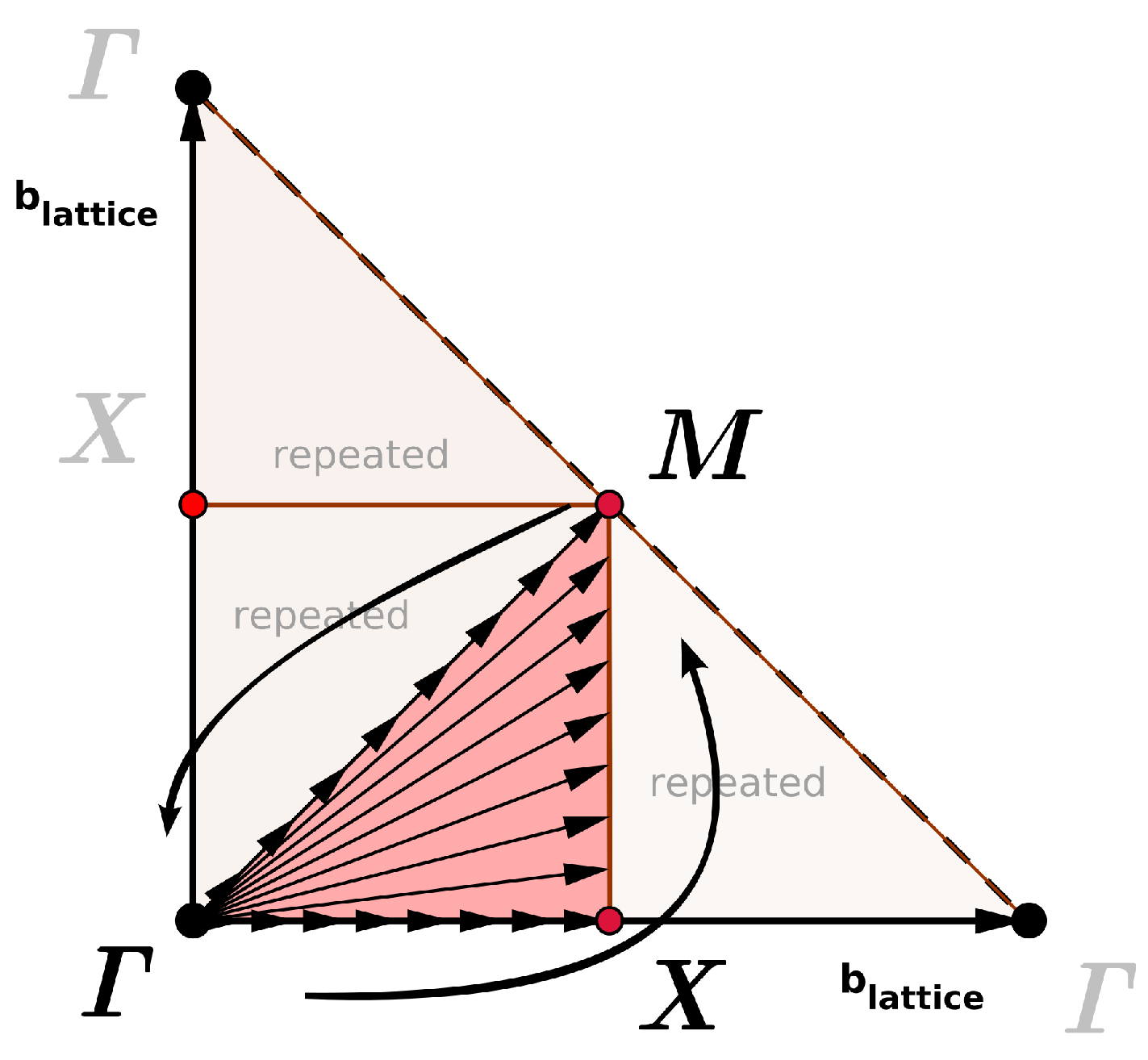


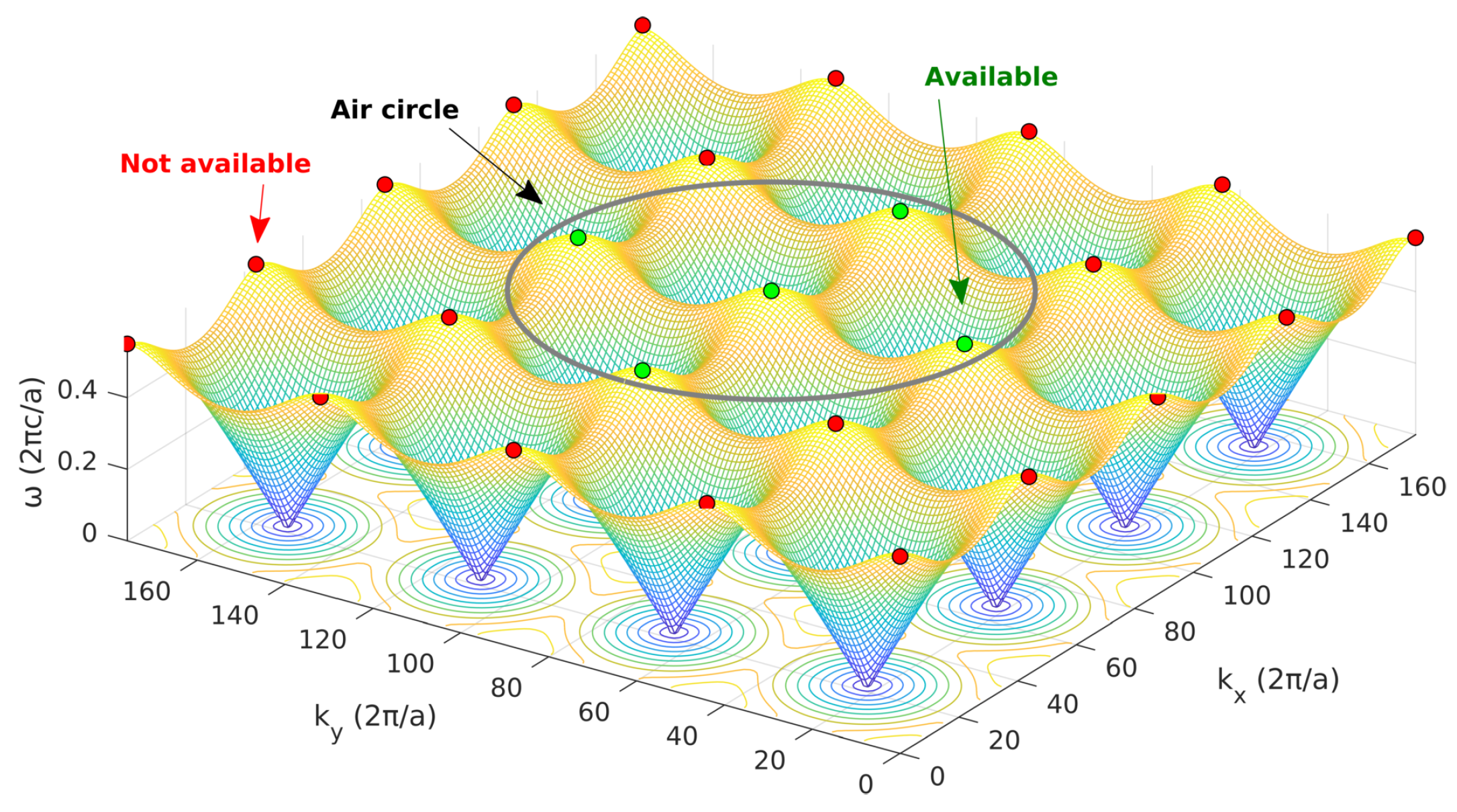
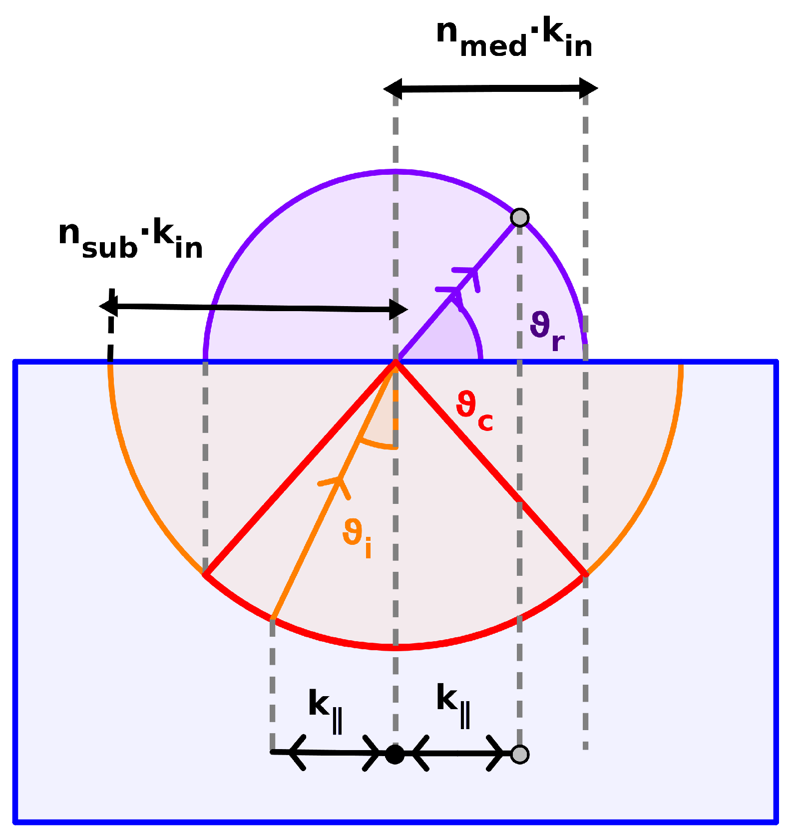


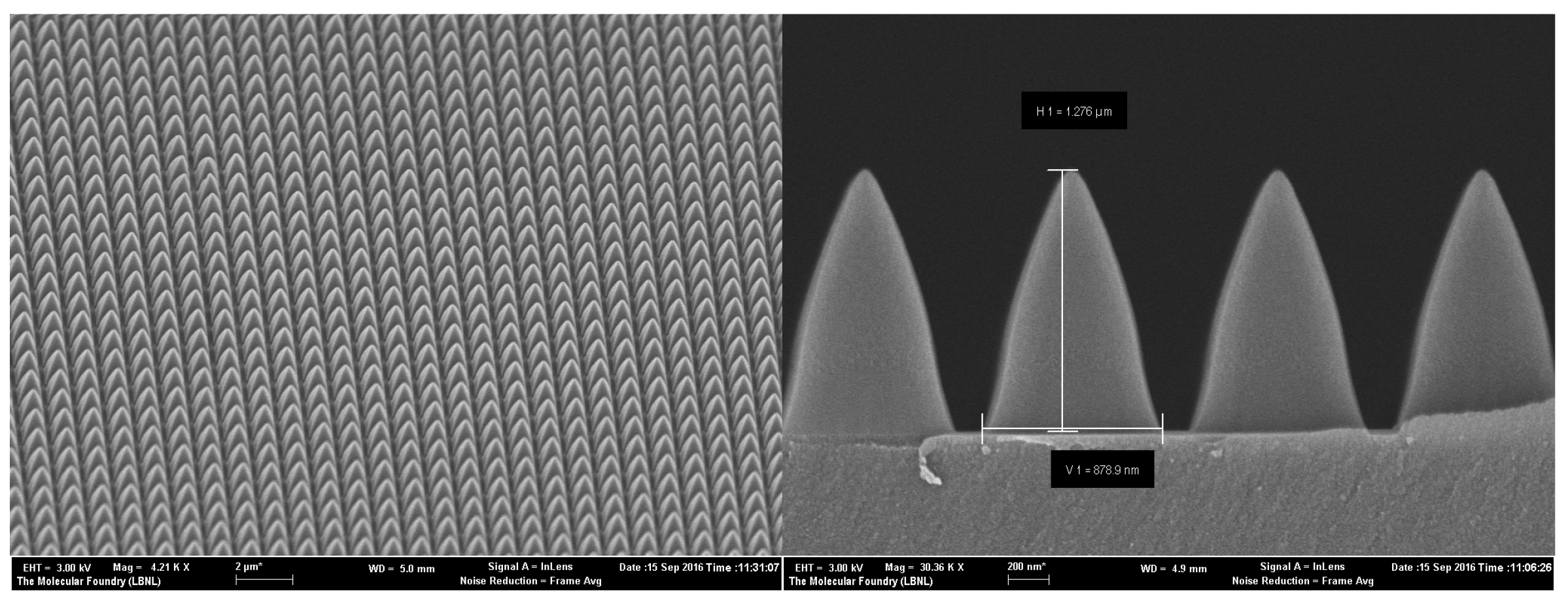

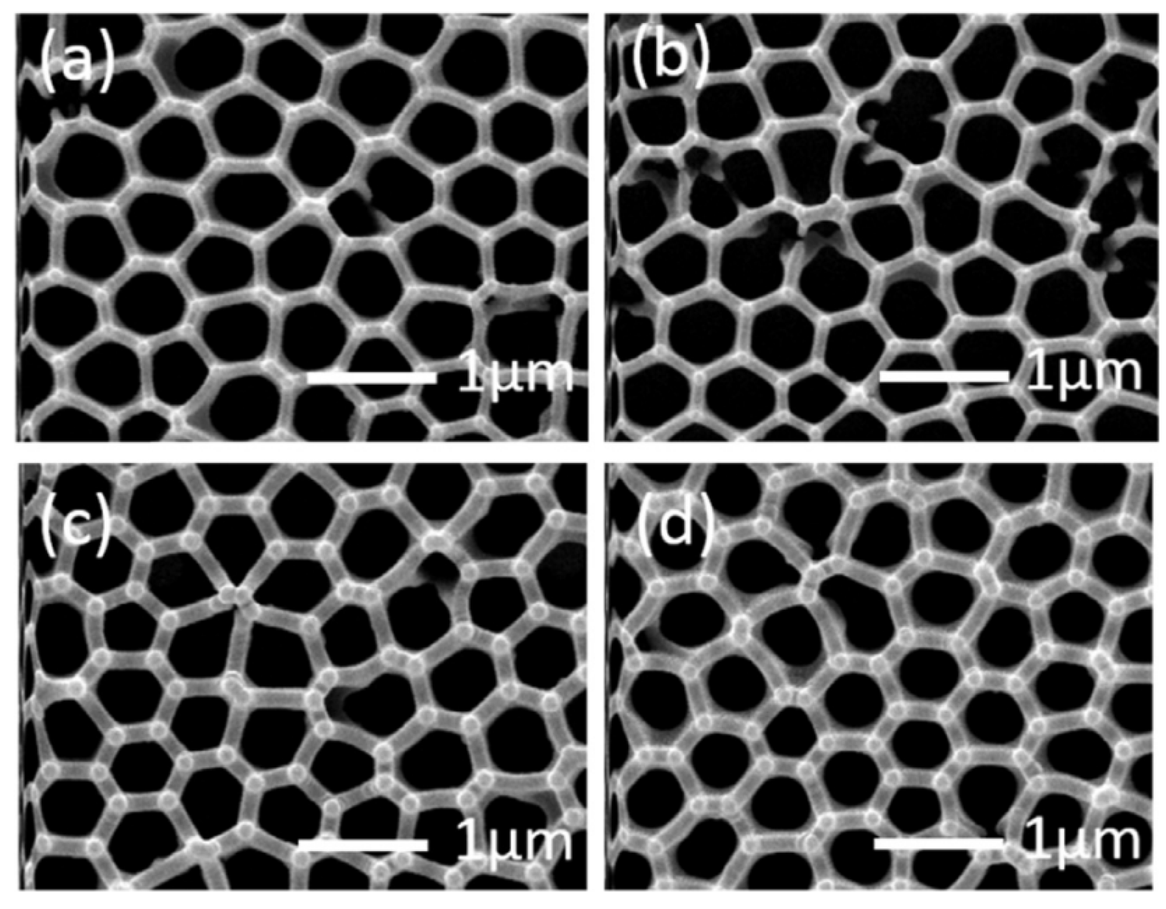
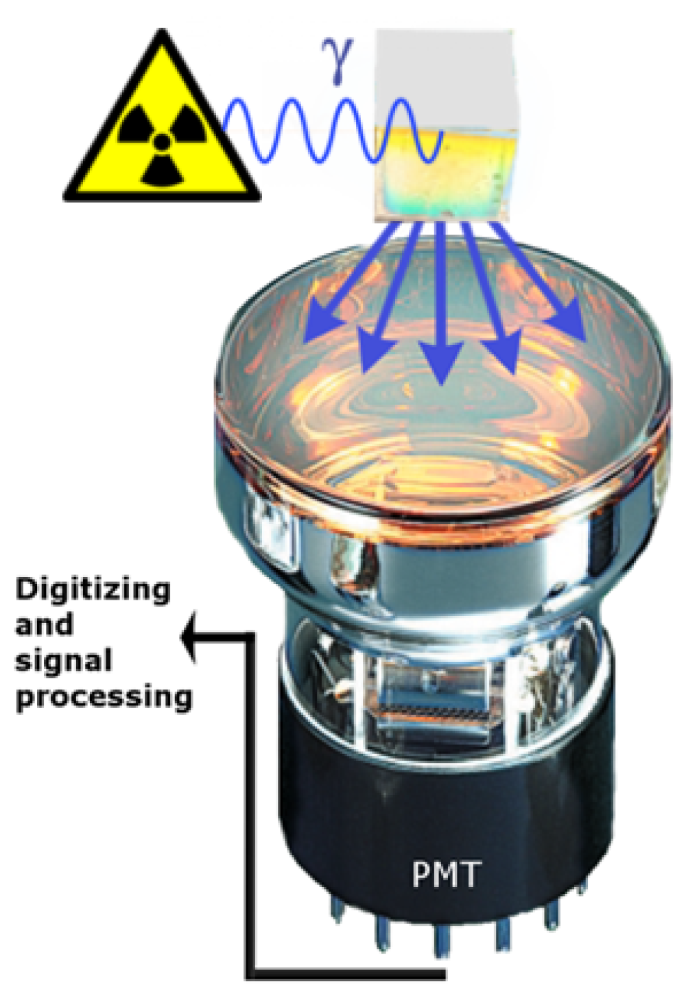


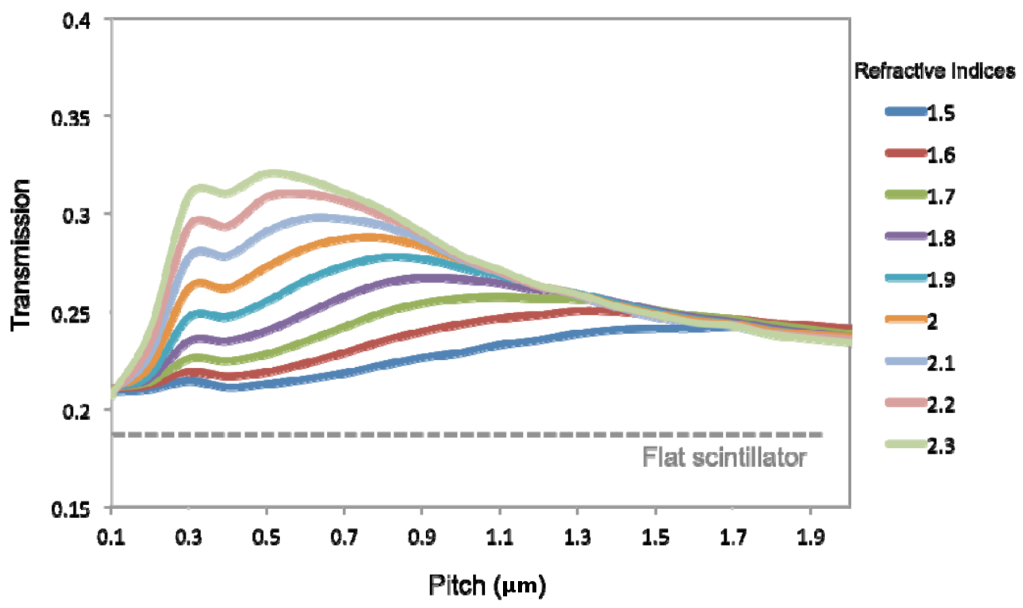
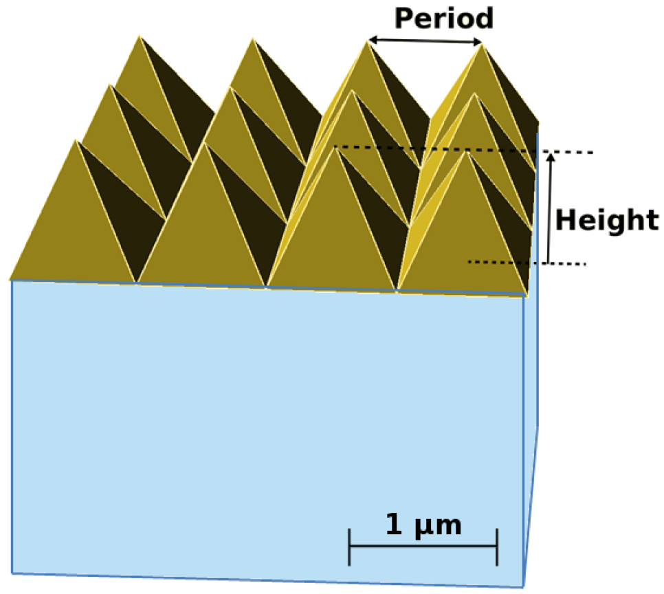


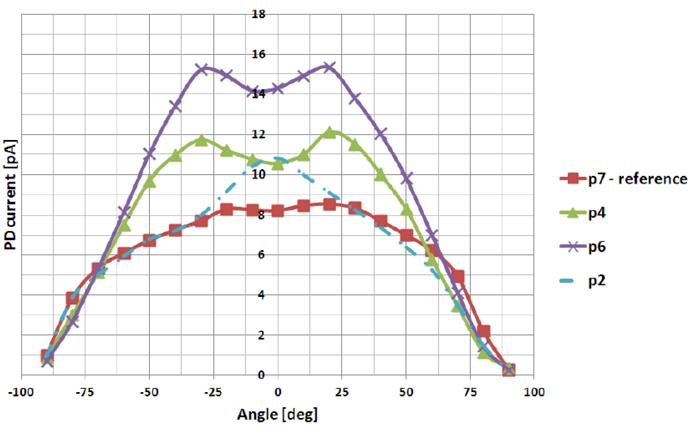
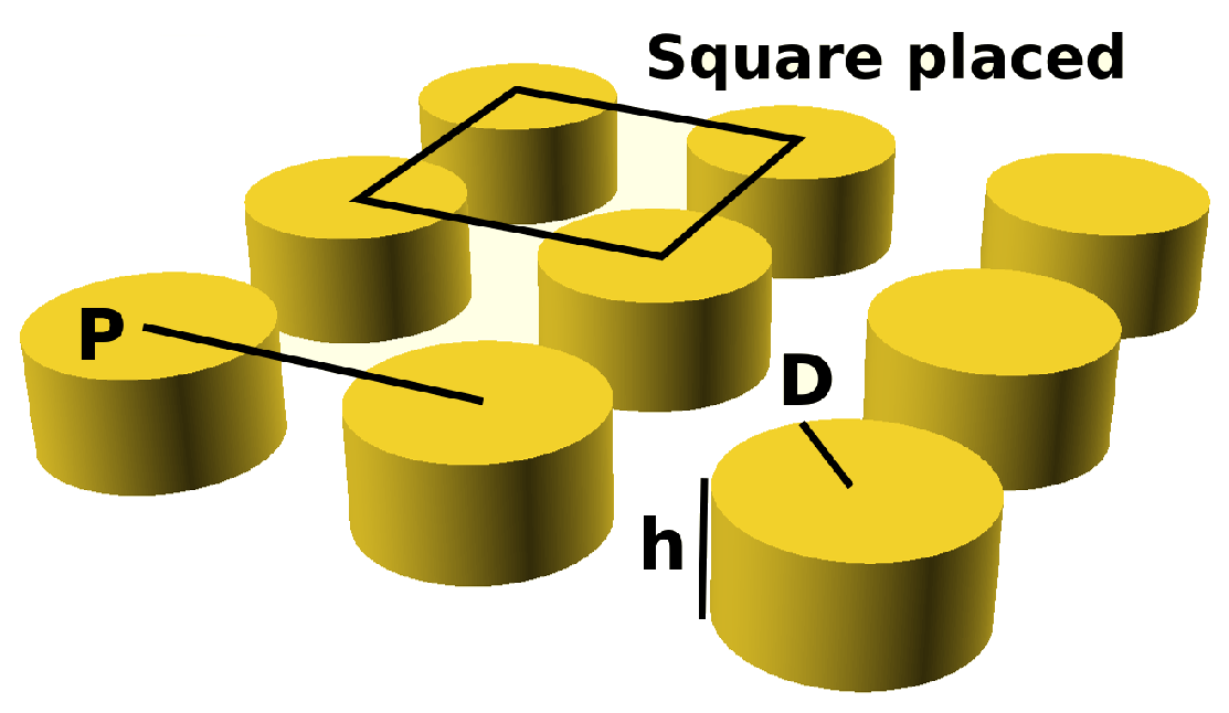
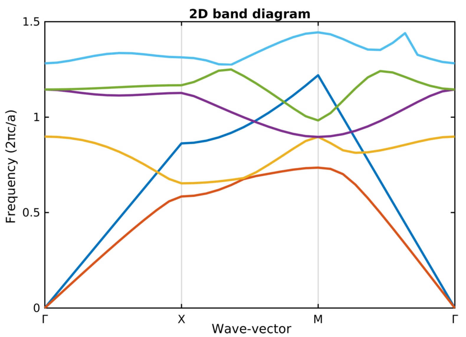
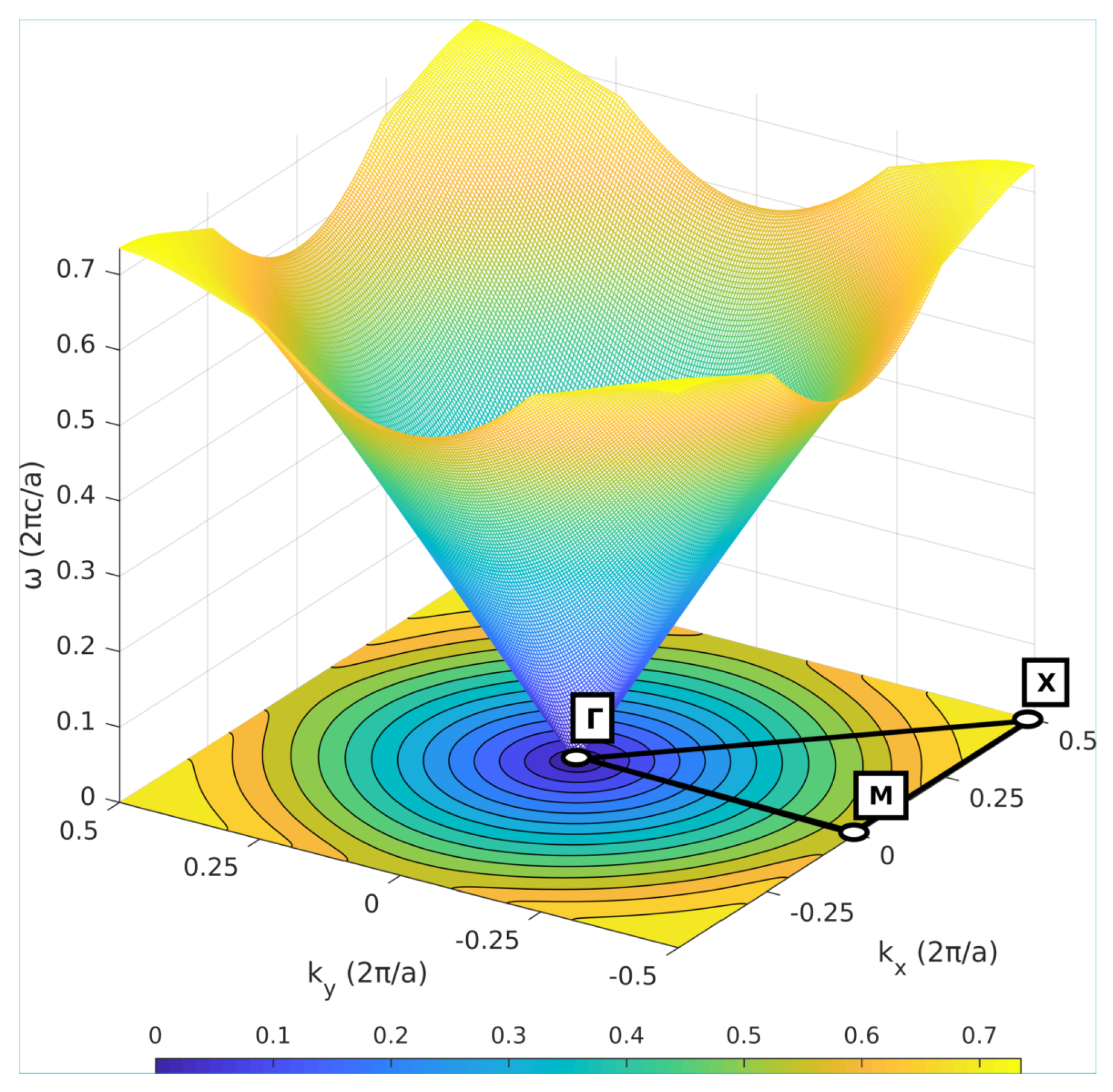
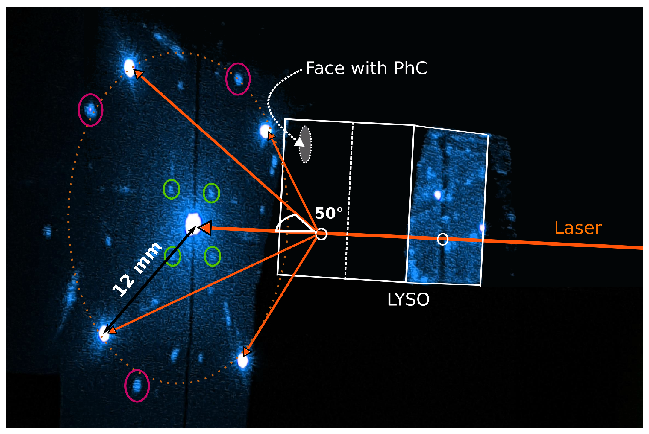
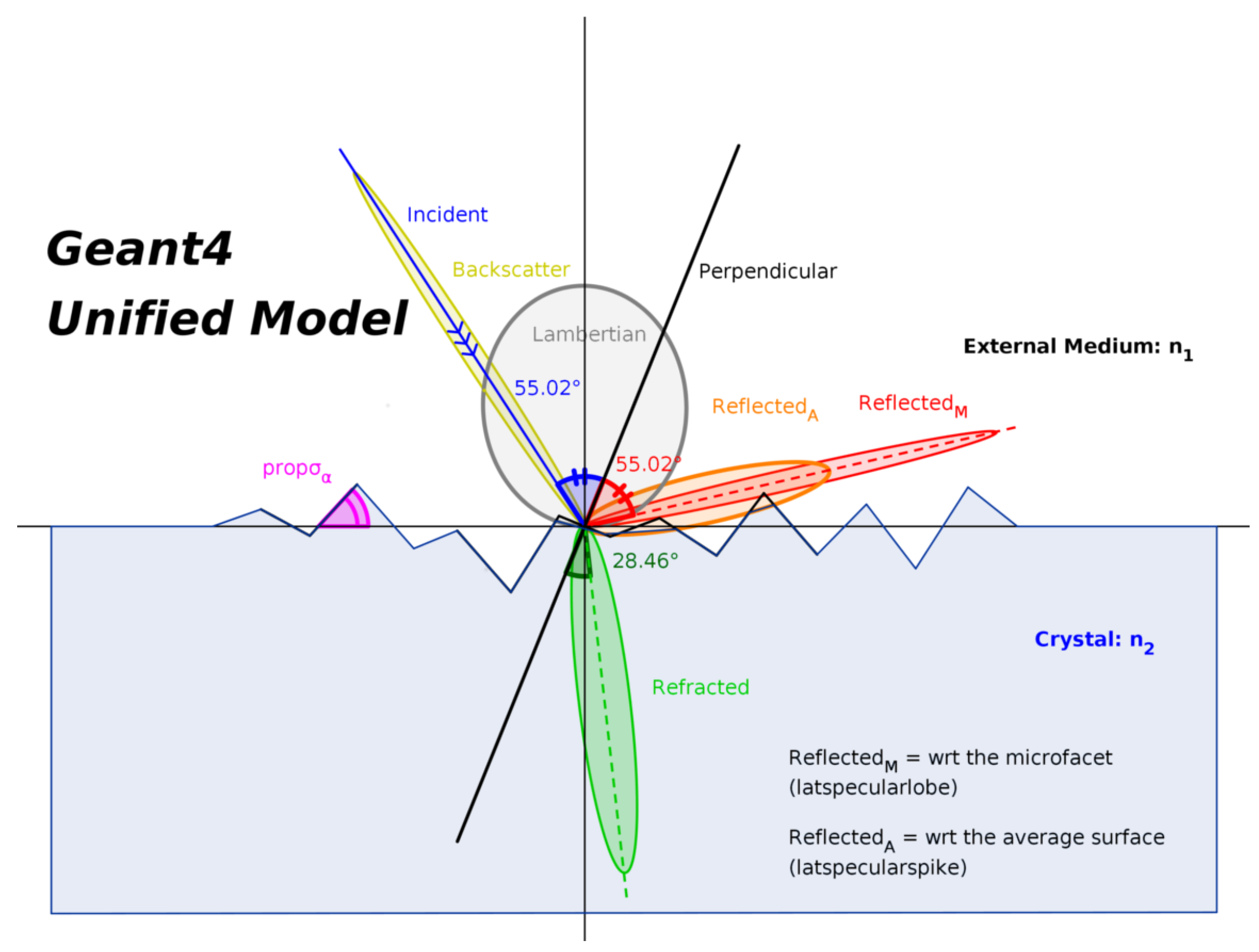
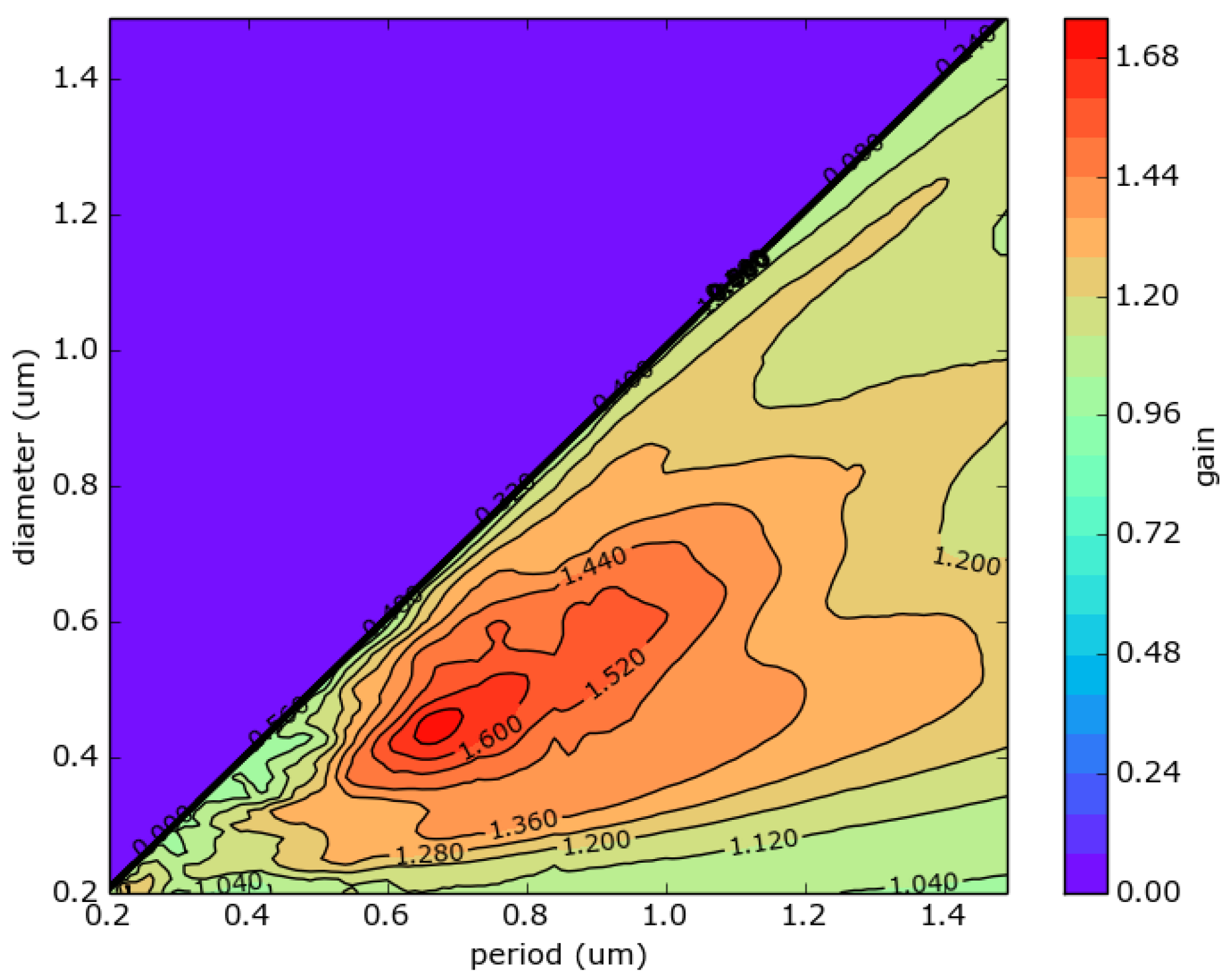
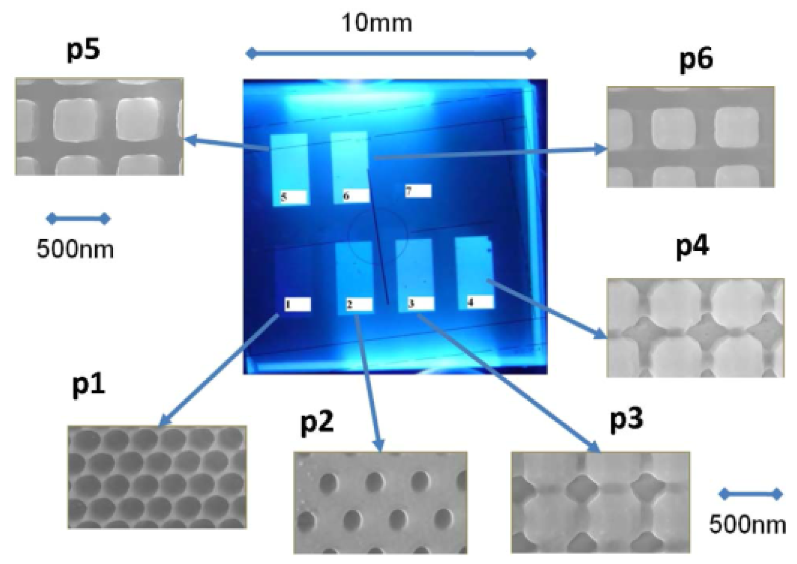
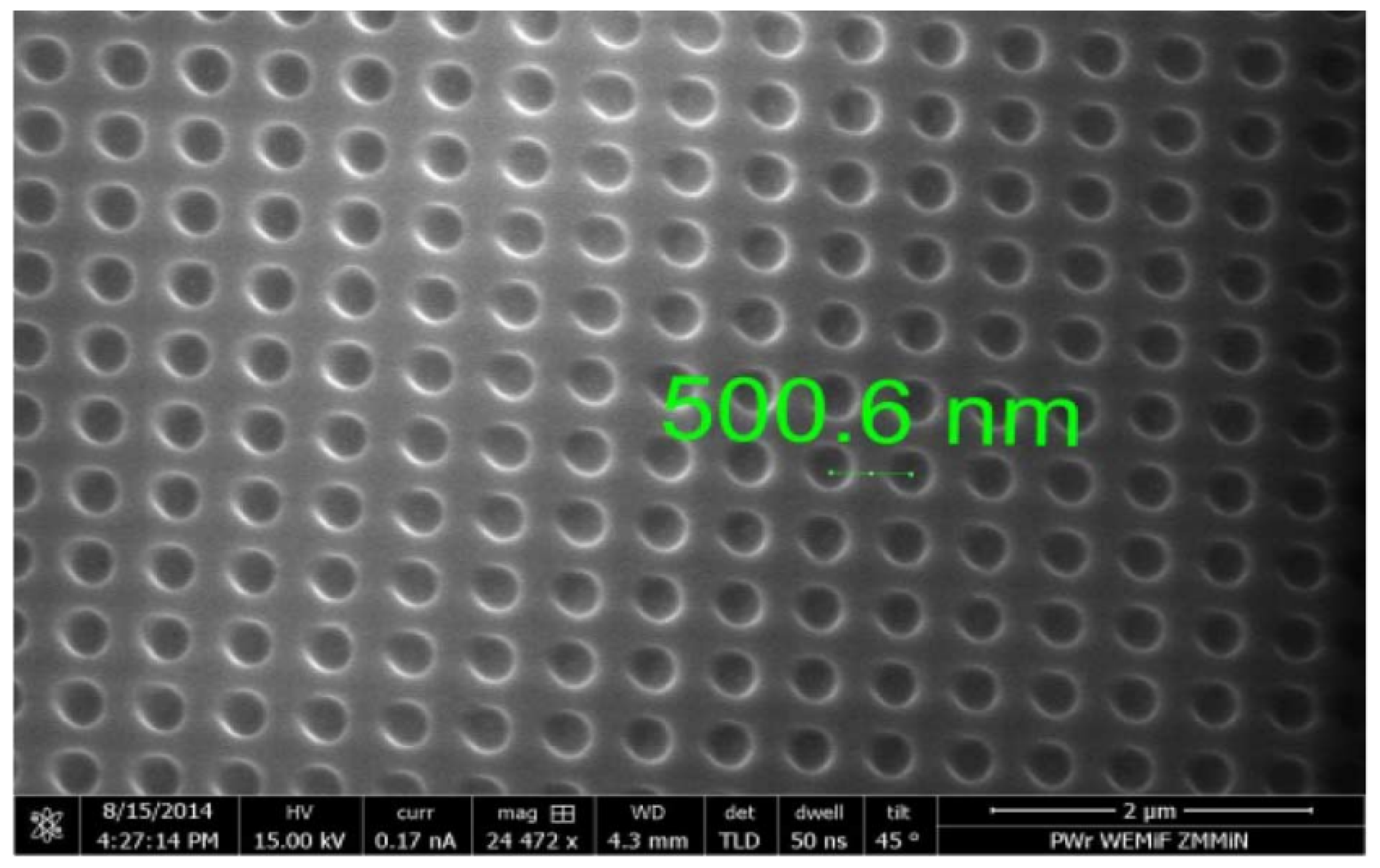
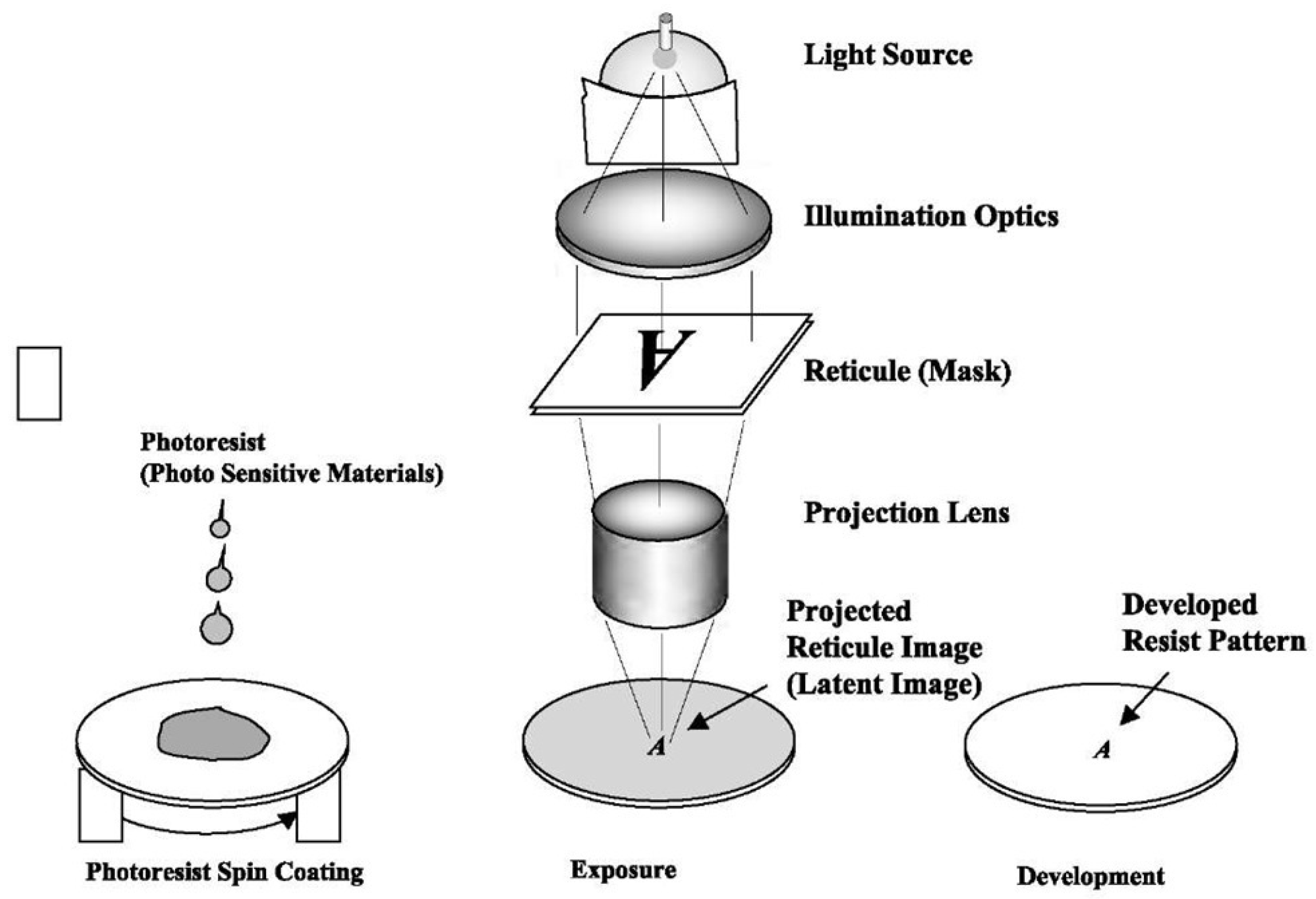
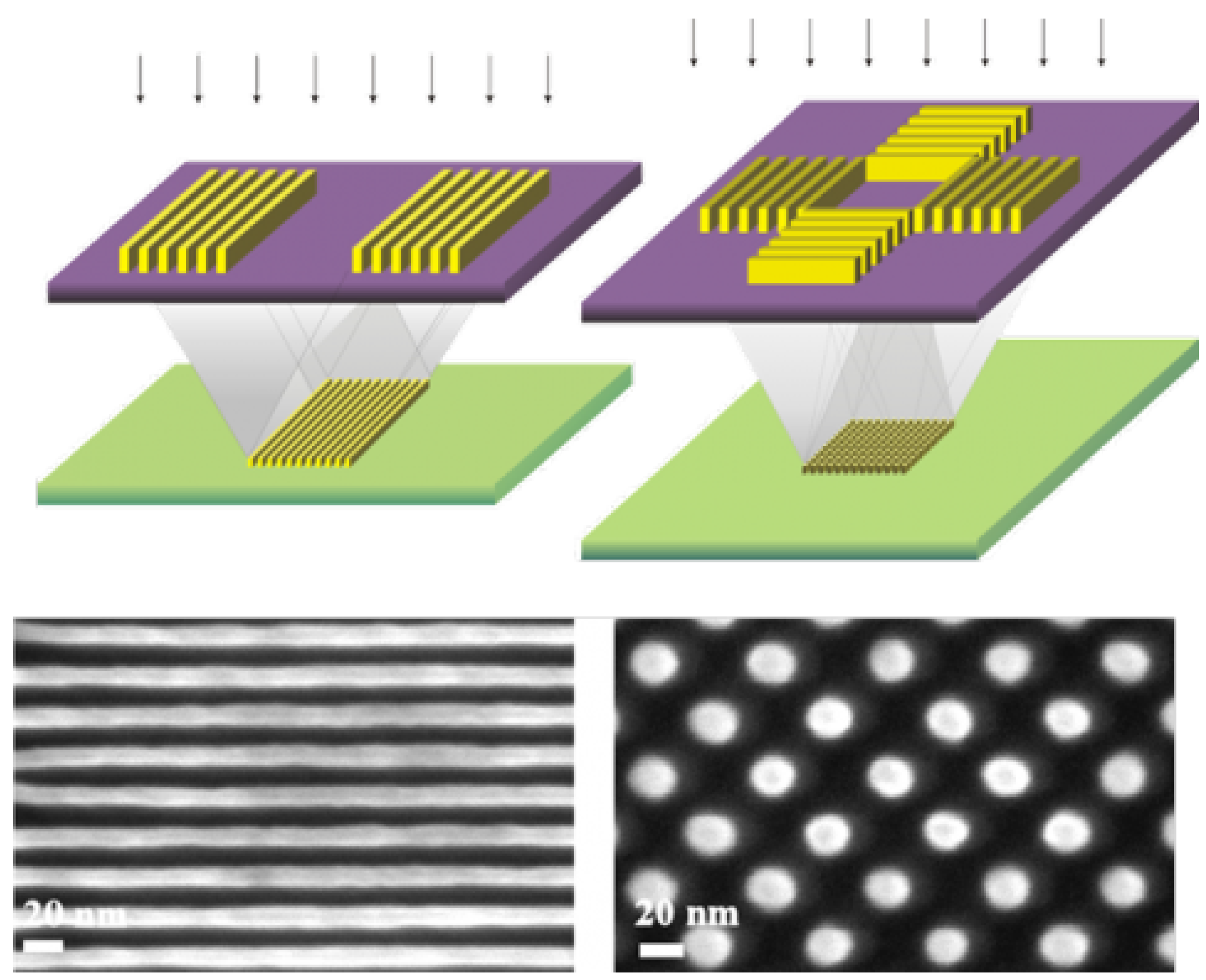
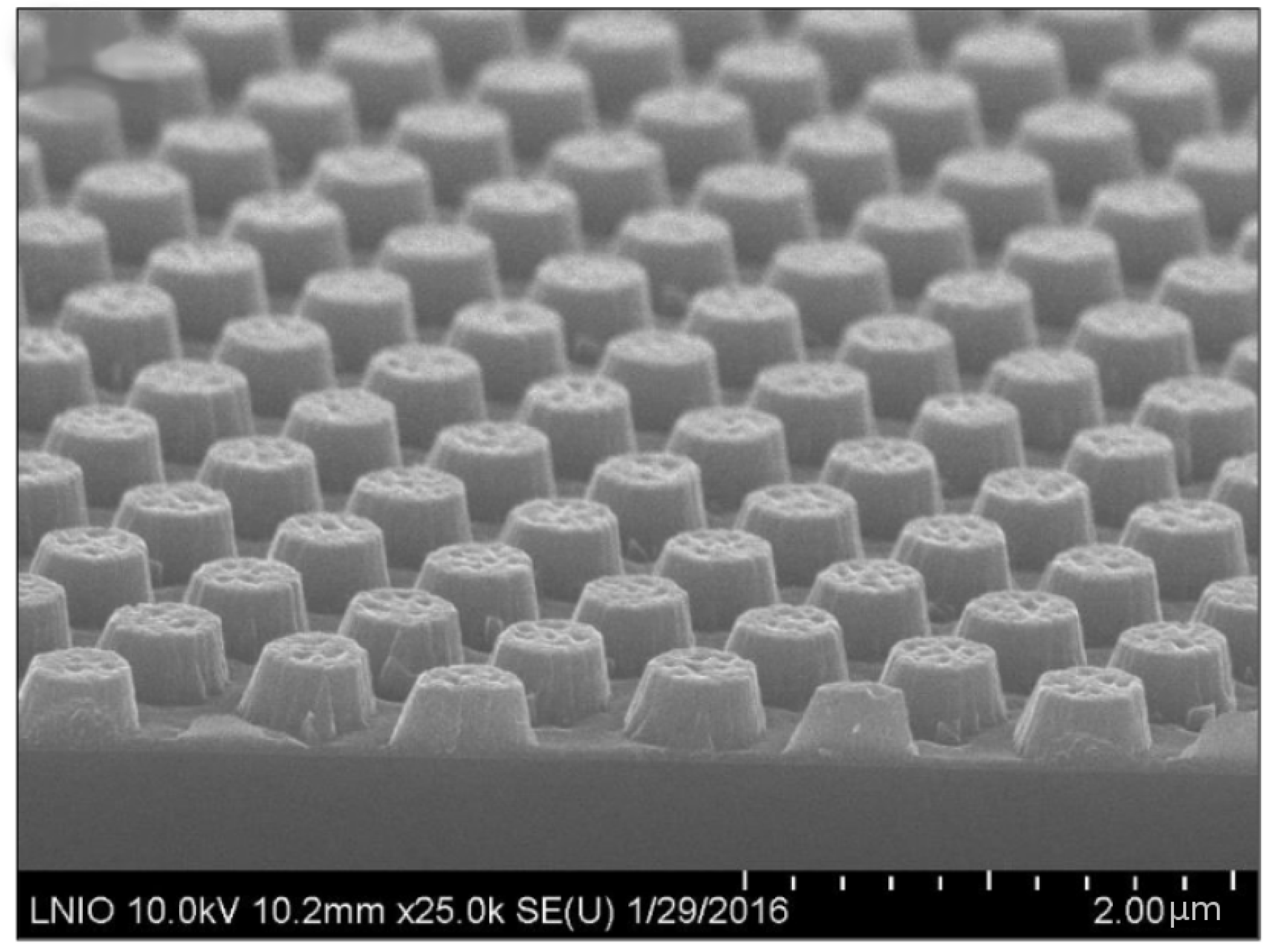
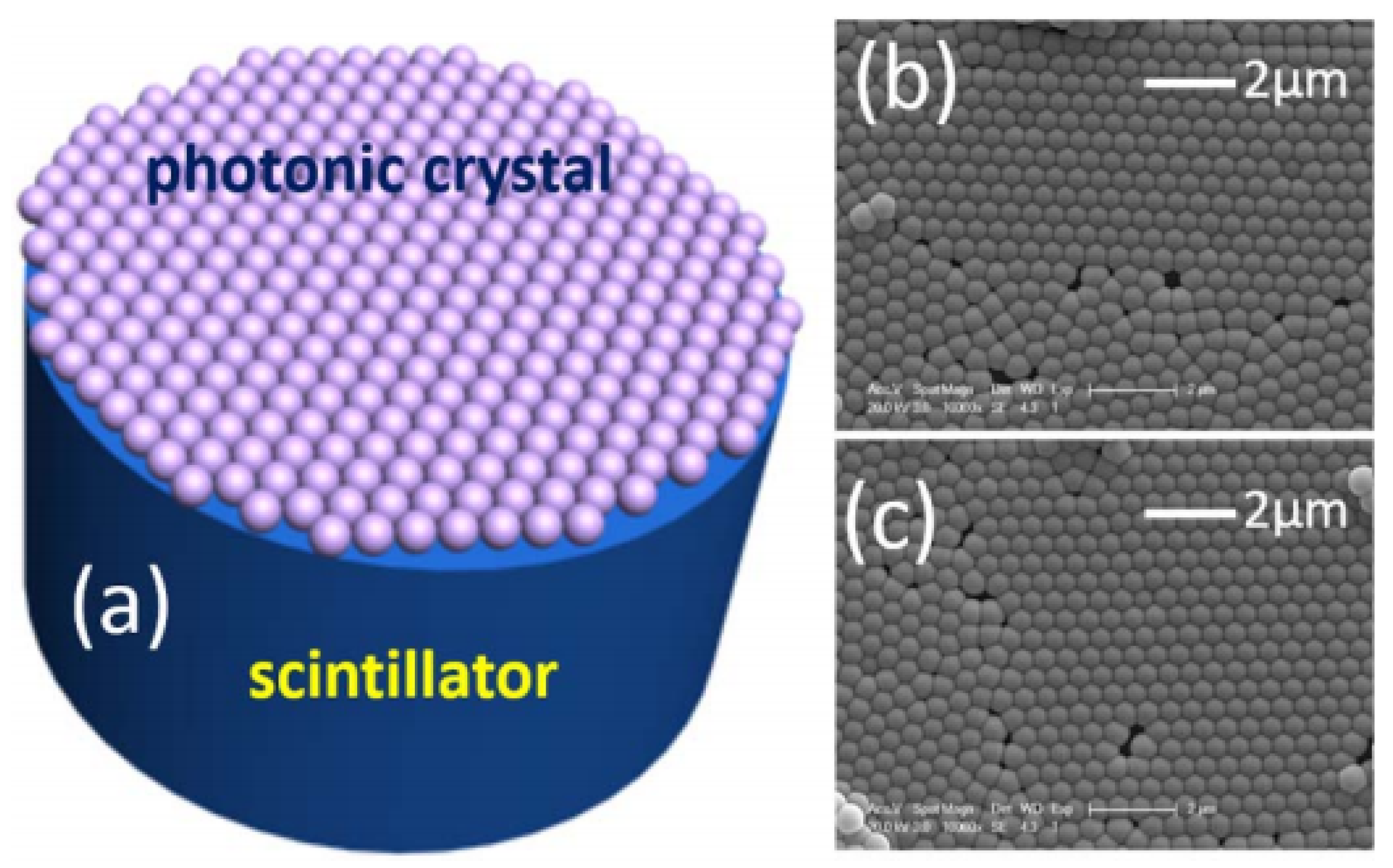
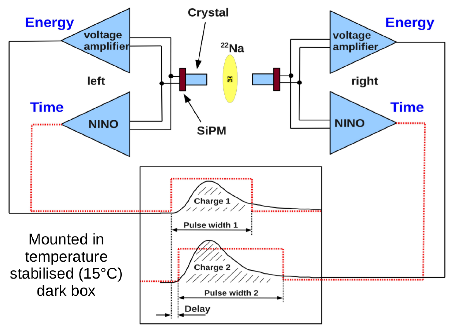
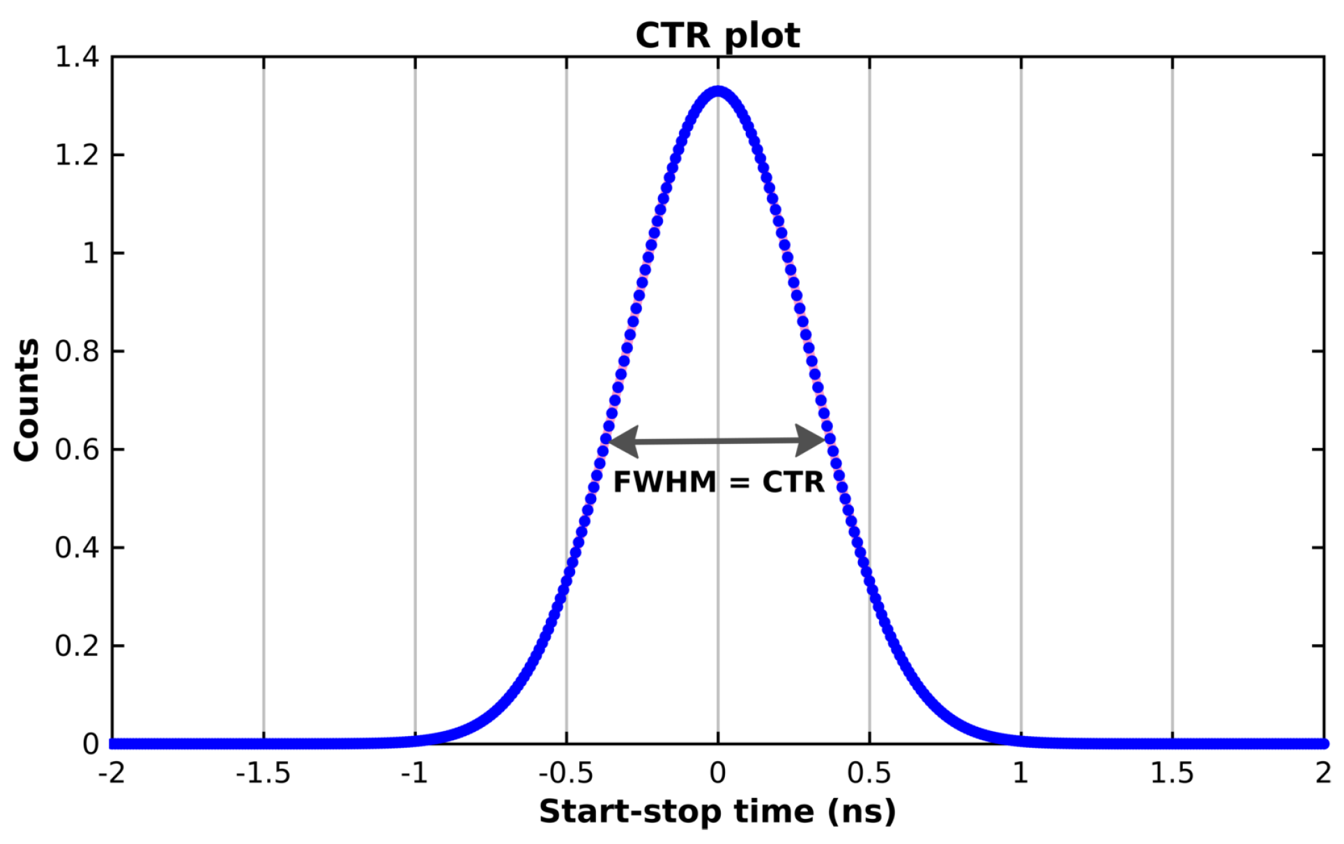
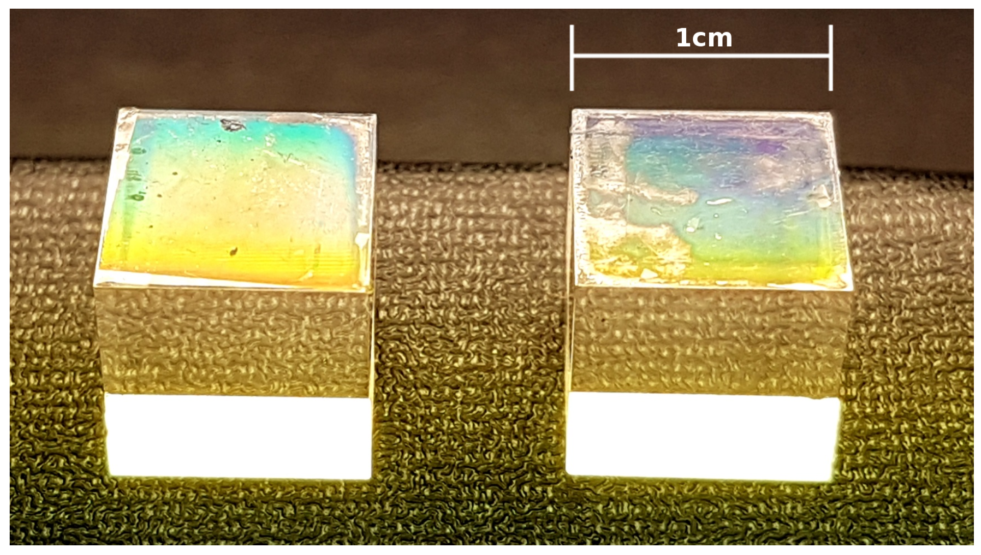