Study on Neutron Irradiation-Induced Structural Defects of GaN-Based Heterostructures

1
School of Electronic and Control Engineering, Chang’an University, Xi’an 710064, China
2
School of Microelectronics, Xidian University, Xi’an 710071, China
3
Key Laboratory of Opto-electronics Technology, Microelectronic School, Beijing University of Technology, Beijing 100124, China
*
Author to whom correspondence should be addressed.
Crystals 2018, 8(5), 198; https://doi.org/10.3390/cryst8050198
Submission received: 25 April 2018
/
Revised: 2 May 2018
/
Accepted: 2 May 2018
/
Published: 3 May 2018
(This article belongs to the Section Crystalline Materials)
Abstract
:The GaN-based heterostructures and related HEMTs (High Electron Mobility Transistors) were investigated by 1MeV neutrons at fluences up to 1015 cm−2, yielding an increase of the densities of screw dislocations and edge dislocations for GaN-based heterostructures. It gave the result that neutron irradiation-induced structural defects into GaN-based materials, and the irradiation-induced dislocations would propagate to the material surface causing surface morphology deterioration. However, the GaN-based material strain was robust to neutrons, and the more initial dislocations, the easier to generate irradiation defects and thus, more strongly affecting the electrical property degradations of materials and devices. Meanwhile, the reduction of the two-dimensional electron gas (2DEG) concentration (ns) caused by irradiation-induced defects led to the reducing the drain current. Moreover, the significant degradation of the reverse gate leakage current at fluences ranging from 1014 to 1015 cm−2 could be attributed to the irradiation-induced deep defects. The neutron induced damage was more difficult to anneal recovery than other particles, due to the neutron irradiation-induced deep levels and defect complexes such as defect clusters.
1. Introduction
GaN-based materials are ideal materials for manufacturing electronic devices with high-voltage, high-temperature and high-frequency applications, due to its superior comprehensive performances; another feature of GaN-based heterostructures and devices is that they have the potential capability to exhibit extremely high radiation hardness. So, GaN-based devices will be a better candidates for applications in outer space and other radiation environment [1,2], where the devices have to operate reliably when subjected to irradiations of protons, γ-rays, or neutrons. There had been considerable effort to understand the nature of radiation defects in GaN-based heterostructures [3,4,5]. Different from γ-rays and protons, when neutrons irradiate semiconductor materials, they generate not only point defects in the materials, but also defect complexes such as defect clusters, and it is the latter, not the point defect, that is most likely to be generated [6].
Polyakov et al. [7] reported the neutron irradiation effects on electrical properties of AlGaN/GaN heterostructures. They found that the mobility/concentration product started to decrease appreciably after the fluence of 1015 cm−2. John et al. [8] found that the formation process of displacement damage was closely related to temperature by low temperature neutron irradiation on AlGaN/GaN HEMTs. Gaubas et al. [9] studied neutron irradiation of the ammonothermal GaN and analyzed the influence of defects induced by neutron irradiation on the carrier lifetime. Our research group [10] found that the fast neutron irradiation of GaN PIN diodes caused the carrier removal effect at the low reverse bias.
It can be seen that most of the current research on neutron irradiation effects of GaN-based heterostructures are focusing on the degradation phenomenon such as the electron mobility or device parameters caused by irradiations. Much less has been done to study the effects of neutron irradiation-induced structural defects on GaN-based heterostructures. However, a clear understanding of the radiation response of structural defects, especially to different initial material quality will provide important and necessary background knowledge for the radiation reinforcement of GaN-based devices. Therefore, in this work, neutron irradiation effects on the self-developed GaN-based heterostructures and related HEMTs (High Electron Mobility Transistors) are studied by means of analyzing the surface morphology, crystal quality of GaN-based materials and annealing characteristics of HEMTs before and after the irradiation.
2. Materials and Experiments
In Figure 1, the HEMT device structure of the fabricated AlGaN/GaN heterostructure is presented. It was grown by metal organic chemical vapor deposition (MOCVD) developed by ourself on (0001) sapphire substrates. The structure was grown unintentionally doped. A 40 nm low temperature GaN (LT-GaN) nucleation layer was initially grown, followed by the deposition of a 100 nm high temperature AlN (HT-AlN) insertion layer. Then 1.65 μm of undoped GaN (UID-GaN) buffer layer and 24 nm n-Al0.3Ga0.7N barrier layer were grown in sequence. The Al0.3Ga0.7N barrier layer was composed of 50 Å undoped Al0.3Ga0.7N, 140 Å doped Al0.3Ga0.7N (Siconcentration = 5 × 1017 cm−3) and 50 Å undoped Al0.3Ga0.7N. The samples contained an additional 10 Å AlN inter layer located between the Al0.3Ga0.7N barrier and GaN channel to reduce alloy scattering. The source-drain ohmic contactswere formed with a Ti (30 nm)/Al (120 nm)/Ti (40 nm)/Au (40 nm) structure. These contacts were annealed at 900 °C for 40 s using rapid thermal anneal in nitrogen atmosphere. A 1000 nm SiN passivation layer was performed by employing PECVD. Using Ni (50 nm)/Au (150 nm) for the gate electrode fabrication. The gate lengths (Lg) were 1 μm, with gate width (Wg) of 100 μm. The source-to-gate and gate-to-drain spaces were both 2 μm.
The GaN-based heterostructures and related HEMTs samples were irradiated at room temperature by fast (1 MeV) neutrons at fluences up to 1015 cm−2. The material and device properties were tested after irradiations. After neutron irradiation, we used off-line testing to get the effect of neutron on the materials characteristics. Firstly, the crystal quality and surface topography of the related GaN-based heterostructures were studied by Bruker D8 Discover X-ray diffractometer and Agilent 5500 AFM, respectively. Then, the No. 1 sample with more initial structural defects and No. 2 sample with less initial structural defects are selected for the radiation experiments. The effects of neutron on the ns (the two-dimensional electron gas concentration), μ (the mobility of the two-dimensional electron gas) and the series resistance Rsh were studied by Hall measurements. While neutron irradiation, an on-line testing on dc characteristics was processed at room temperature using a HP 4155 parameter analyzer. Annealing was carried out at room temperature for 20 h in air.
3. Results and Discussion
Figure 2 and Table 1 show XRD rocking curves and the corresponding FWHMs of (002) and (102) planes for GaN-based heterostructures before and after 1015 cm−2 neutrons irradiation, respectively. It can be seen that the FWHMs of both samples increase after irradiation, and that of the (102) planes, it shifts more significantly. As the FWHM of the (002) (the (102)) plane corresponds to densities of screw dislocations (edge dislocations) [11,12], the densities of edge dislocations show a larger increment after the irradiation, which indicates that neutron irradiation introduces structural defects (especially edge dislocations) into GaN-based materials. In our previous neutron irradiation studies, the neutron-irradiated GaN-based heterostructures samples also exhibited much greater yellow luminescence (YL) intensities as shown in Figure 3. It is considered that neutron irradiation-induced structural defects such as vacancies and dislocations are major factors in deteriorating the performance of materials [6,10,13,14,15].
The FWHM shifts of the No. 1 sample are more noticeable than that of the No. 2 sample, which means that the sample with more initial structural defects would increases more defects after the irradiation, while the one with less initial structural defects will be considerably more radiation-hardened.
Figure 4 shows XRD ω-2θ scanning curves of GaN-based heterostructures made by the No. 1 sample before and after 1015 cm−2 neutrons. It can be seen that the position of the GaN peak almost remains the same as before neutron irradiation, which indicates that neutron irradiation has little effect on the material strain at fluencies up to 1015 cm−2.
Figure 5 shows the surface morphology changes of the GaN-based heterostructures made by No. 1 sample investigated by AFM before and after 1015 cm−2 neutrons. Table 2 lists the main normalized parameters (including the normalized roughness mean square RMS, the normalized surface pit density ρ and the normalized surface pit diameter d). It can be seen that after neutron irradiation, RMS, ρ and d of the materials increase, and the surface morphology deteriorates.
The results of XRD and AFM also show that the initial materials with high quality have a small degradation while the initial materials with poor quality have a relatively large degradation. Because the irradiation is more likely to generate point defects or defect complexes at dislocations, the more initial dislocations, the easier to generate irradiation defects and thus, more strongly affecting the electrical property degradations of materials and devices. For further verifications, the neutron irradiation analysis is performed on HEMTs fabricated with No. 1 and No. 2 samples, respectively. Figure 6 shows the transfer characteristics of the two HEMTs before and after neutron irradiation; we can find the HEMT made by No. 1 sample have a more degradation than the HEMT made by No. 2 sample after neutron irradiation. It is considered that irradiation-induced defects are crucial reasons for the reduction of the saturation drain current.
Table 3 lists the results of Hall measurements at 300K. After neutron irradiation, the ns (the two-dimensional electron gas concentration) of the GaN-based heterostructures declines, the series resistance Rsh rises, while the μ (the mobility of the two-dimensional electron gas) increases slightly. Consistent with AFM and XRD measurements, No. 1 sample has a more radiation degradation. The μ increases slightly after the irradiation mainly due to the modulation of carrier concentrations. The 2DEG expands into GaN after neutron irradiation, reducing the confinement of the heterostructure interface, that is, the shielding effect of carriers on ionized impurities and the phonon scattering grows, so μ rises slightly after the irradiation. The ns decrease caused by irradiation-induced defects leads to the reduction of the drain current.
The reverse gate characteristics of HEMTs have degraded obviously after neutron irradiation, as shown in Figure 7. It can be seen that the reverse gate leakage current reduces obviously after neutron irradiation, and the higher the fluences, the more the reverse gate leakage current degrades. Unlike γ-raysand protons [16,17], neutrons react directly with the nucleus, so deep trap defects or defect complexes are easily formed in the material [6,10,13,14,15]. Once these deep defects trap the gate electrons, the electrons can hardly be detrapped, so at this time, the mechanism of traps is mainly attributed to the carrier removal effect of the deep defects. On the other hand, these electrons are trapped which also obstructs the movement of subsequent electrons, thereby reducing the injection of gate electrons, and decreasing the reverse gate current.
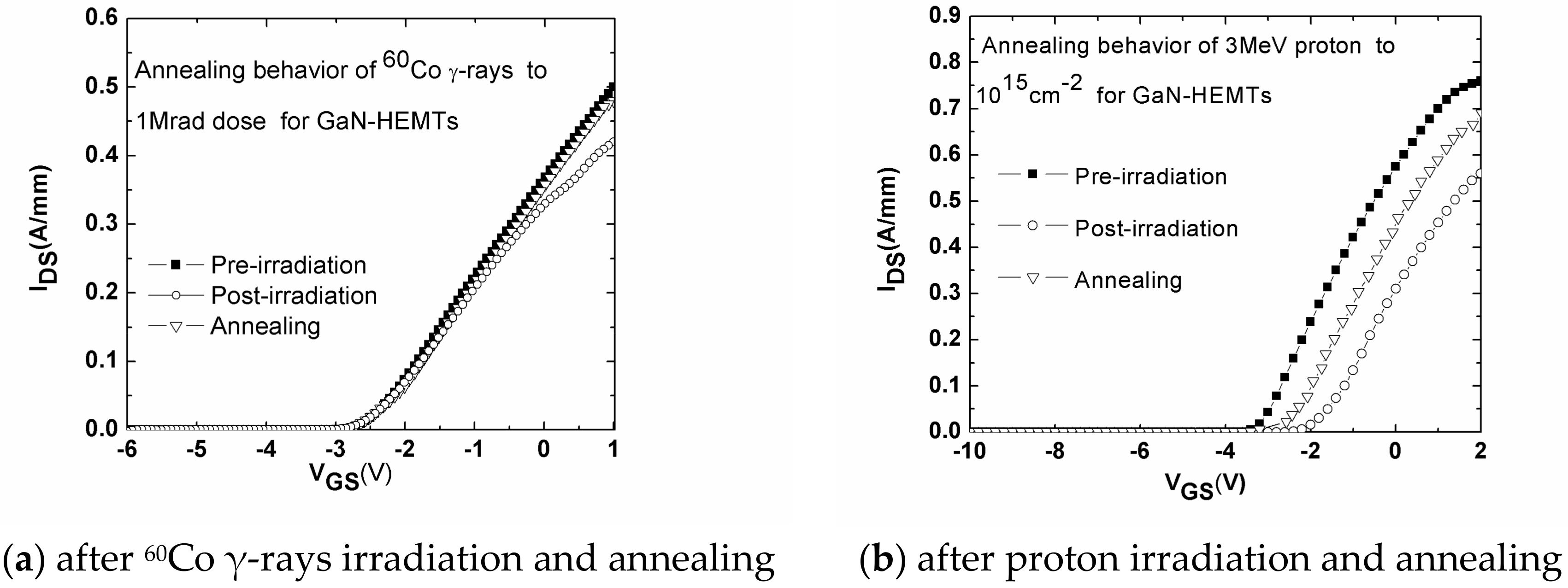
After the irradiation, the HEMTs made by No. 1 sample were annealed at room temperature to further observe the properties of neutron irradiation-induced defects. Figure 8 shows the reverse gate characteristics as the anneal time for HEMTs after 1015 cm−2 neutrons. We do not observe any significant annealing recovery effect on this time scale on remeasured samples, but the parameters also continue to degrade a little, which is completely different from the results of the obvious recovery phenomenon observed in previous irradiation annealing studies [18]. So, 60Co γ-rays and protons irradiation annealing experiments have also been carried out for GaN-based HEMTs at room temperature, as shown in Figure 9. After the irradiations of the two kinds of particles, both HEMTs show good annealing recovery. The analysis suggests that the damage caused by γ-rays or protons is generally easier to anneal recovery than neutrons. Protons and γ-rays irradiation at high energy can produce simple point defects in the lattice, while neutrons irradiation can create extended defects. The neutrons displace atoms in the crystal lattice, inducing structural defects such as vacancies, interstitial atoms, dislocations and defect complexes in GaN-based materials [6,10,15,16,17]. The neutron irradiation-induced defects are easily combined with the structural defects of the materials to form defect complexes during annealing at room temperature, which further degrades the device characteristics, so the neutron annealing recovery was more difficult. Furthermore, comparing Figure 6 and Figure 9, the proton irradiation seems to affect IDS more strongly than neutron irradiation, because the NIEL (Non-ionizing energy loss) of 1 MeV neutron irradiation is an order of magnitude lower than 3 MeV proton [19].
4. Conclusions
The above experimental results show that after neutron irradiation, the GaN-based heterostructure material strain almost remains the same, but the densities of screw dislocations and edge dislocations increase. Neutron irradiation introduces structural defects into GaN-based materials, and the irradiation-induced dislocations would propagate to the material surface, which causes surface morphology deterioration. By analyzing neutron irradiation effects on the heterostructures and HEMTs with different initial structural defect distributions, it is found that the more initial dislocations, the easier it is to generate irradiation defects, thus, more strongly affecting the electrical property degradations of materials and devices. The ns reducing caused by the irradiation-induced defects leads to the reduction of the drain current. Neutron irradiation frequently induces deep levels and defect complexes, and the neutron-induced damage is more difficult to anneal recovery than γ-rays or protons.
Author Contributions
Wenping Gu is responsible for the overall experimental design and manuscript writing. Xiaobo Xu and Lin Zhang have performed specific annealing experiments. Zhiyuan Gao has performed some material characterizations. Xiaochuan Hu and Zan Zhang have conducted data processing.
Acknowledgments
This work was supported by National natural science foundation of China (NO. 6150401, No. 11705014, No. 41101357), Natural Science Basic Research Plan in Shaanxi Province of China (No. 2017JQ6042) the fundamental research funds for the central universities (No. 300102328111) and the Science and Technology Program of Xi’an, China (Grant No. 2017088CG/RC051(CADX005)).
Conflicts of Interest
The authors declare no conflicts of interest.
References
- Collins, K.C.; Armstrong, A.M.; Allerman, A.A.; Vizkelethy, G.; van Deusen, S.B.; Leonard, F.; Talin, A.A. Proton irradiation effects on minority carrier diffusion length and defect introduction in homoepitaxial and heteroepitaxial n-GaN. J. Appl. Phys. 2017, 122. [Google Scholar] [CrossRef]
- Lei, Z.F.; Guo, H.X.; Tang, M.H.; Zeng, C.; Zhang, Z.G.; Chen, H.; En, Y.F.; Huang, Y.; Chen, Y.Q.; Peng, C. Degradation mechanisms of AlGaN/GaN HEMTs under 800 MeV Bi ions irradiation. Microelectron. Reliabil. 2018, 80, 312–316. [Google Scholar] [CrossRef]
- Chen, J.; Puzyrev, Y.S.; Zhang, C.X.; Zhang, E.X.; McCurdy, M.W.; Fleetwood, D.M.; Schrimpf, R.D.; Pantelides, S.T.; Kaun, S.W.; Kyle, E.C.H.; et al. Proton-induced dehydrogenation of defects in AlGaN/GaN HEMTs. IEEE Trans. Nuclear Sci. 2013, 60, 4080–4086. [Google Scholar] [CrossRef]
- Kumar, A.; Singh, R.; Kumar, P.; Singh, U.B.; Asokan, K.; Karaseov, P.A.; Titov, A.I.; Kanjilal, D. In-situ transport and microstructural evolution in GaN Schottky diodes and epilayers exposed to swift heavy ion irradiation. J. Appl. Phys. 2018, 123. [Google Scholar] [CrossRef]
- Kurakin, A.M.; Vitusevich, S.A.; Danylyuk, S.V.; Hardtdegen, H.; Klein, N.; Bougrioua, Z.; Danilchenko, B.A.; Konakova, R.V.; Belyaev, A.E. Mechanism of mobility increase of the two-dimensional electron gas in AlGaNGaN heterostructures under small dose gamma irradiation. J. Appl. Phys. 2008, 103. [Google Scholar] [CrossRef]
- McClory, J.W. The Effect of Radiation on Electrical Properties of Aluminum Gallium Nitride/Gallium Nitride Heterostructures; Technology Air University: Dayton, OH, USA, 2008. [Google Scholar]
- Polyakov, A.Y.; Smirnov, N.B.; Govorkov, A.V.; Markov, A.V.; Pearton, S.J.; Kolin, N.G.; Merkurisov, D.I.; Boiko, V.M. Neutron irradiation effects on electrical properties and deep-level spectra in undoped n-AlGaN/GaN heterostructures. J. Appl. Phys. 2005, 98. [Google Scholar] [CrossRef]
- McClory, J.W.; Petrosky, J.C. Temperature Dependent Electrical Characteristics of Neutron Irradiated AlGaN/GaN HFETs; Institute of Electrical and Electronics Engineers Inc.: Piscataway, NJ, USA, 2007; pp. 1969–1974. [Google Scholar]
- Gaubas, E.; Ceponis, T.; Deveikis, L.; Meskauskaite, D.; Miasojedovas, S.; Mickevicius, J.; Pavlov, J.; Pukas, K.; Vaitkus, J.; Velicka, M.; et al. Study of neutron irradiated structures of ammonothermal GaN. J. Phys. D Appl. Phys. 2017, 50, 135102. [Google Scholar] [CrossRef]
- Lv, L.; Li, P.; Ma, X.; Liu, L.; Yang, L.; Zhou, X.; Zhang, J.; Cao, Y.; Bi, Z.; Jiang, T.; Zhu, Q.; Hao, Y. Fast and Thermal Neutron Radiation Effects on GaN PIN Diodes. IEEE Trans. Nucl. Sci. 2017, 64, 643–647. [Google Scholar] [CrossRef]
- Xu, Z.H.; Zhang, J.C.; Zhang, Z.F.; Zhu, Q.-W.; Duan, H.-T.; Hao, Y. The effects of vicinal sapphire substrates on the properties of AlGaN/GaN heterostructures. Chin. Phys. B 2009, 18, 5457. [Google Scholar]
- Chandolu, A.; Song, D.Y.; Holtz, M.E.; Gherasoiu, I.; Nikishin, S.A.; Bernussi, A.; Holtz, M.W. X-ray diffraction and photoluminescence studies of InN grown by plasma-assisted molecular beam epitaxy with low free-carrier concentration. J. Electron. Mater. 2009, 38, 557–562. [Google Scholar] [CrossRef]
- Zhang, M.L.; Wang, X.L.; Xiao, H.L.; Yang, C.; Wang, R. Influence of neutron irradiation on the deep levels in GaN, Solid-State and Integrated Circuit Technology. In Proceedings of the 10th IEEE International Conference on Solid-State and Integrated Circuit Technology (ICSICT), Shanghai, China, 1–4 November 2010. [Google Scholar]
- Pearton, S.J.; Deist, R.; Ren, F.; Liu, L.; Polyakov, A.Y.; Kim, J. Review of radiation damage in GaN-based materials and devices. J. Vac. Sci. Technol. A 2013, 35, 050801. [Google Scholar] [CrossRef]
- Lorenz, K.; Marques, J.G.; Franco, N.; Alves, E.; Peres, M.; Correia, M.R.; Monteiro, T. Defect studies on fast and thermal neutron irradiated GaN. Nucl. Instrum. Methods Phys. Res. B Beam Interact. Mater. At. 2008, 266, 2780–2783. [Google Scholar] [CrossRef]
- Roy, T.; Zhang, E.X.; Puzyrev, Y.S.; Fleetwood, D.M.; Schrimpf, R.D.; Choi, B.K.; Hmelo, A.B. Process dependence of protoninduced degradation in GaN HEMTs. IEEE Trans. Nucl. Sci. 2010, 57, 3060–3065. [Google Scholar]
- Lv, L.; Ma, J.G.; Cao, Y.R.; Zhang, J.C.; Li, L.; Xu, S.R.; Ma, X.H.; Ren, X.T.; Hao, Y. Study of proton irradiation effects on AlGaN/GaN high electron mobility transistors. Microelectron. Reliabil. 2011, 51, 2168–2172. [Google Scholar] [CrossRef]
- Cai, S.J.; Tang, Y.S.; Li, R.; Wei, Y.Y.; Wong, L.; Chen, Y.L.; Wang, K.L.; Chen, M.; Zhao, Y.F.; Schrimpf, R.D.; et al. Annealing behavior of a proton irradiated AlxGa1-xN/GaN high electron mobility transistor grown by MBE. IEEE Trans. Electron. Devices 2000, 47, 304–307. [Google Scholar] [CrossRef]
- Summers, G.P.; Burke, E.A.; Dale, C.J.; Wolicki, E.A.; Wolicki, E.A.; Gehlhausen, M.A. Correlation of particle induced displacement damage in silicon. IEEE Trans. Nucl. Sci. 1987, 34, 1133–1139. [Google Scholar] [CrossRef]
Figure 1.
Schematic of AlGaN/GaN HEMT structure.

Figure 2.
Rocking curves of (002) planes for No. 1 sample (a), No. 2 sample (b), and (102) planes for No. 1 sample (c), No. 2 sample (d) before and after 1015 cm−2 neutrons.
Figure 2.
Rocking curves of (002) planes for No. 1 sample (a), No. 2 sample (b), and (102) planes for No. 1 sample (c), No. 2 sample (d) before and after 1015 cm−2 neutrons.
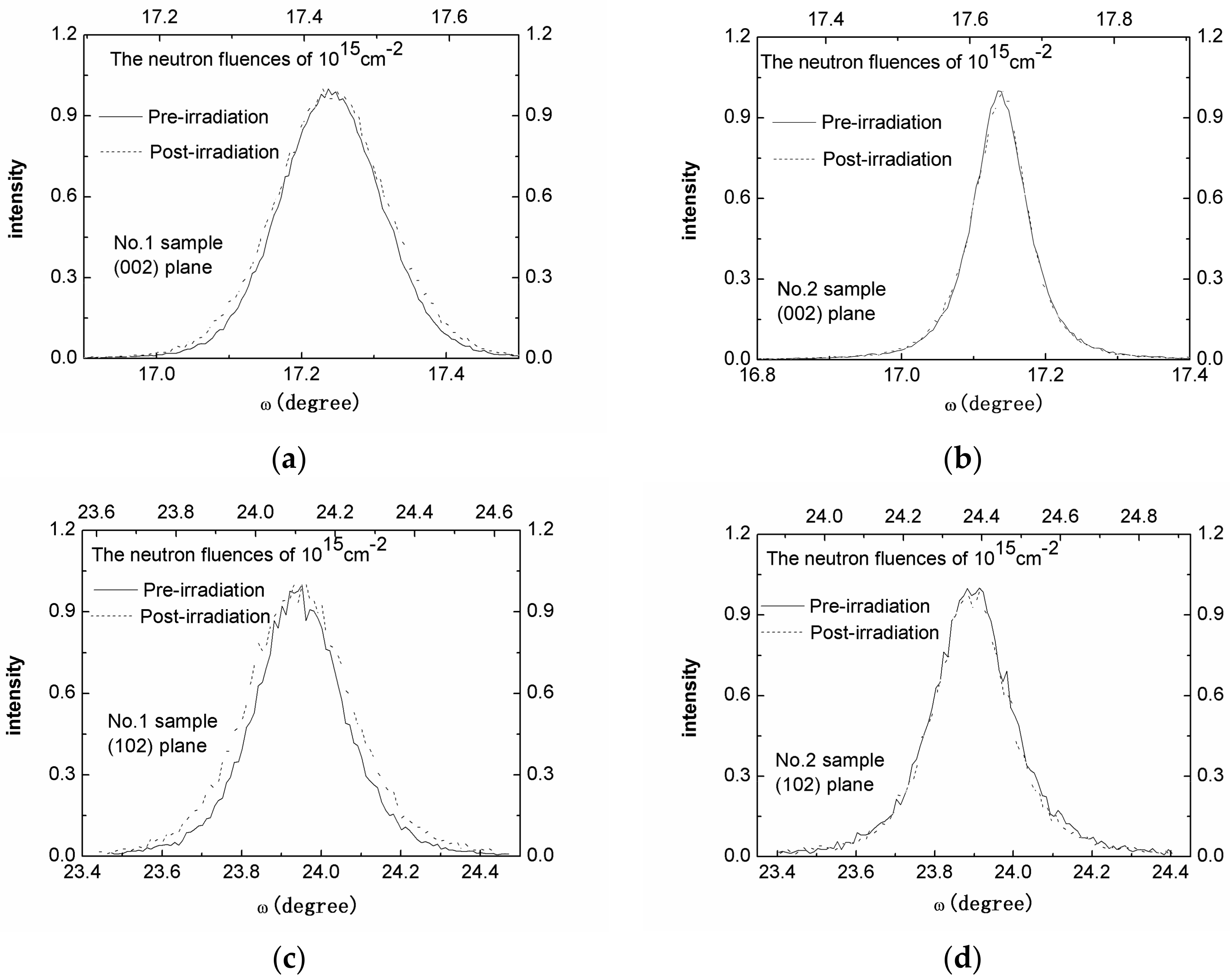
Figure 3.
PL spectrum of the 1MeV neutron-irradiated AlGaN/GaN heterostructures samples.
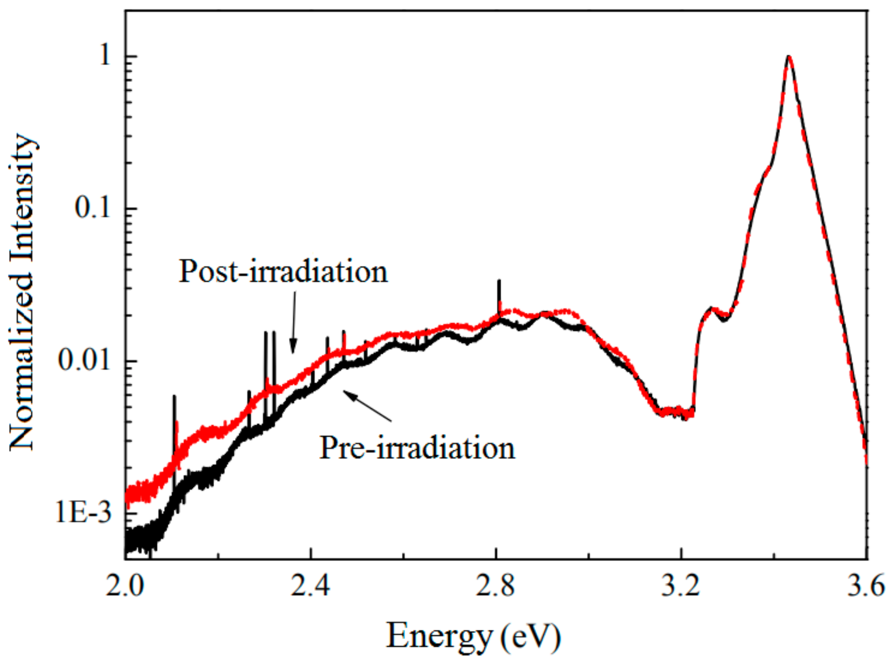
Figure 4.
XRD ω-2θ scanning curves of AlGaN/GaN heterostructures made by No. 1 sample before and after 1015 cm−2 neutrons.
Figure 4.
XRD ω-2θ scanning curves of AlGaN/GaN heterostructures made by No. 1 sample before and after 1015 cm−2 neutrons.
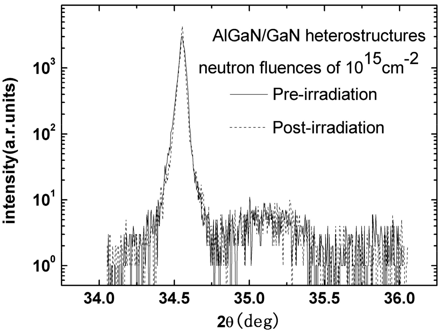
Figure 5.
AFM measurements of AlGaN/GaN heterostructures (2 × 2 μm2) made by the No. 1 sample before and after 1015 cm−2 neutrons.
Figure 5.
AFM measurements of AlGaN/GaN heterostructures (2 × 2 μm2) made by the No. 1 sample before and after 1015 cm−2 neutrons.
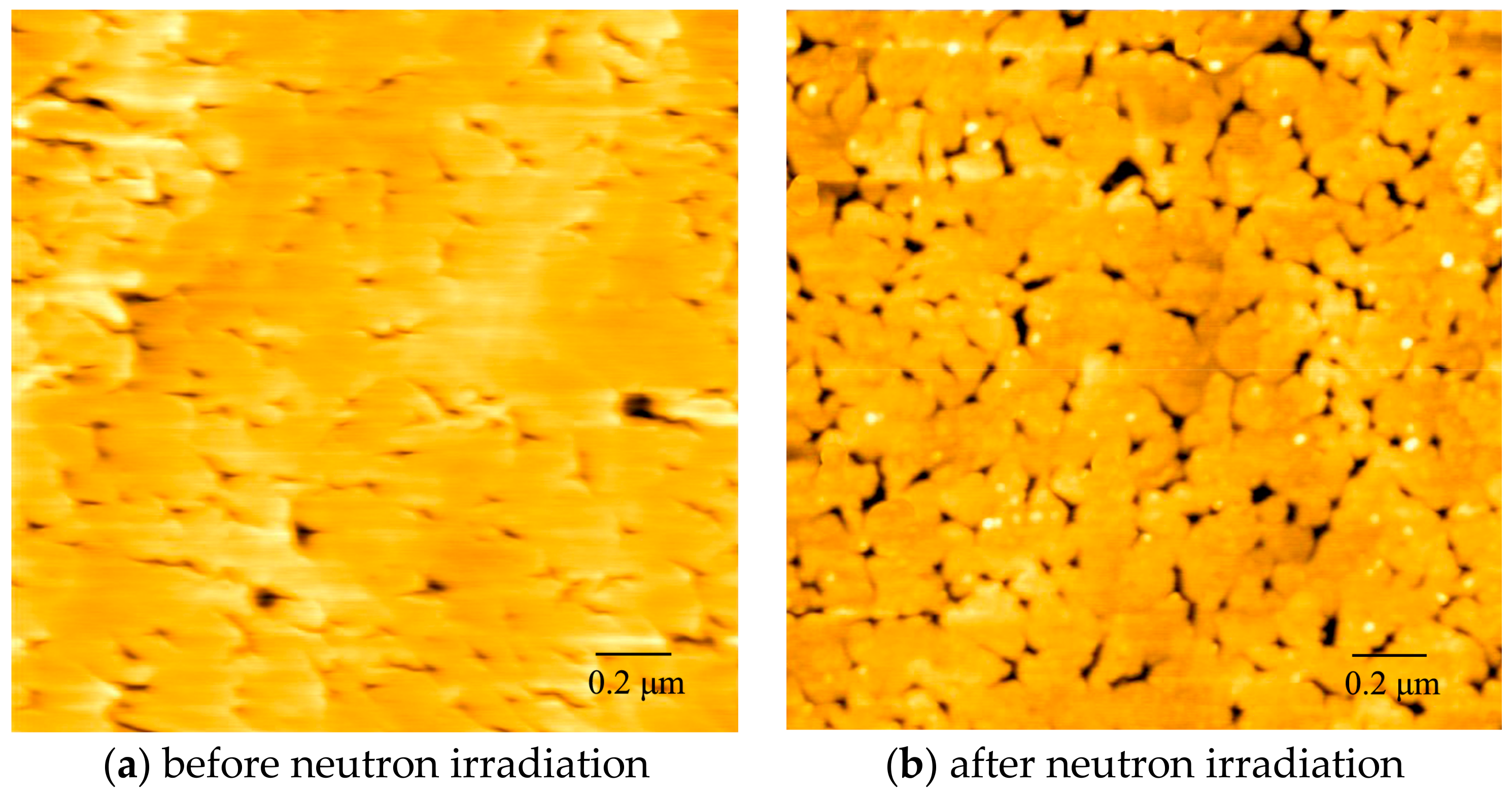
Figure 6.
Transfer characteristics of AlGaN/GaN HEMTs before and after 1015 cm−2 neutrons.
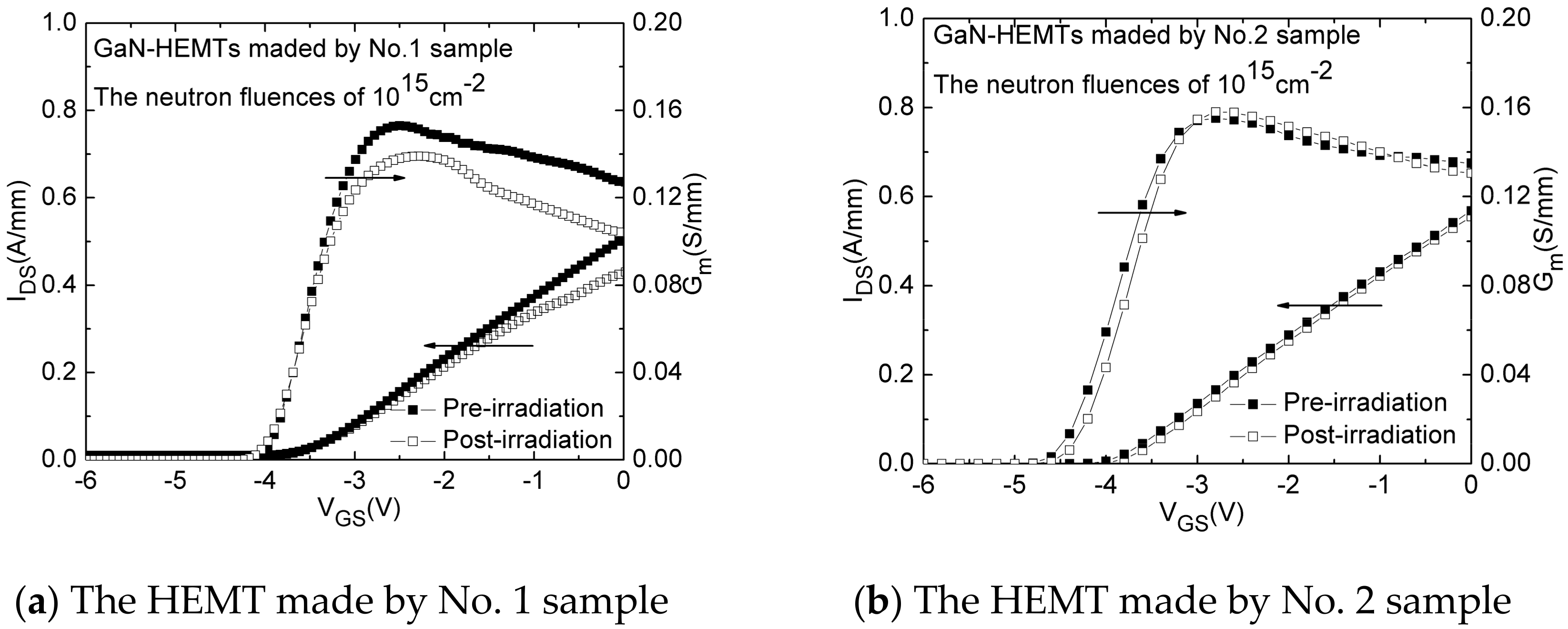
Figure 7.
Reverse gate characteristics from HEMTs (made by No. 1 sample) before and after 1 MeV neutron irradiation at three different fluencies.
Figure 7.
Reverse gate characteristics from HEMTs (made by No. 1 sample) before and after 1 MeV neutron irradiation at three different fluencies.
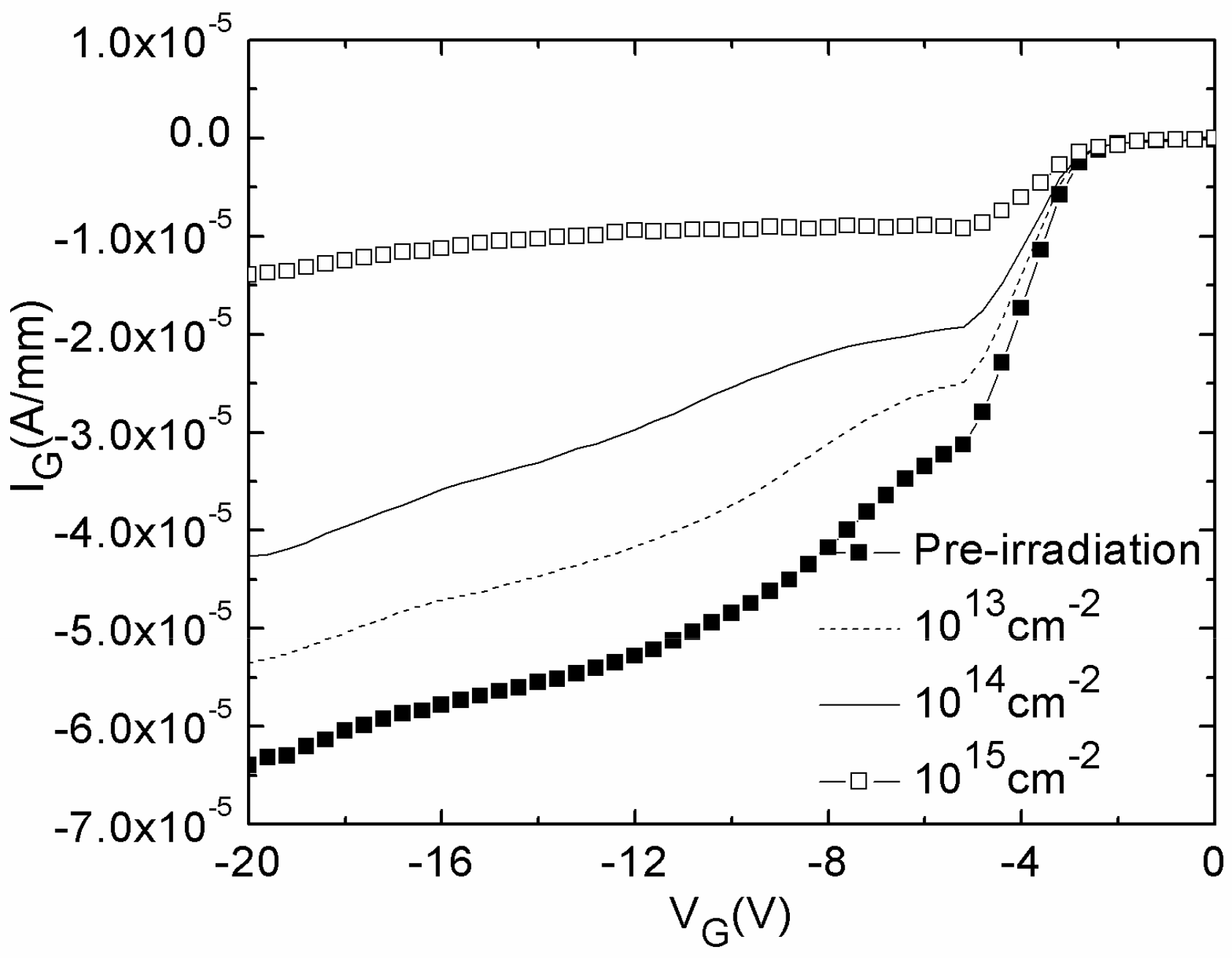
Figure 8.
Reverse gate characteristics as the anneal time for HEMTs (made by No. 1 sample) after 1015 cm−2 neutrons.
Figure 8.
Reverse gate characteristics as the anneal time for HEMTs (made by No. 1 sample) after 1015 cm−2 neutrons.
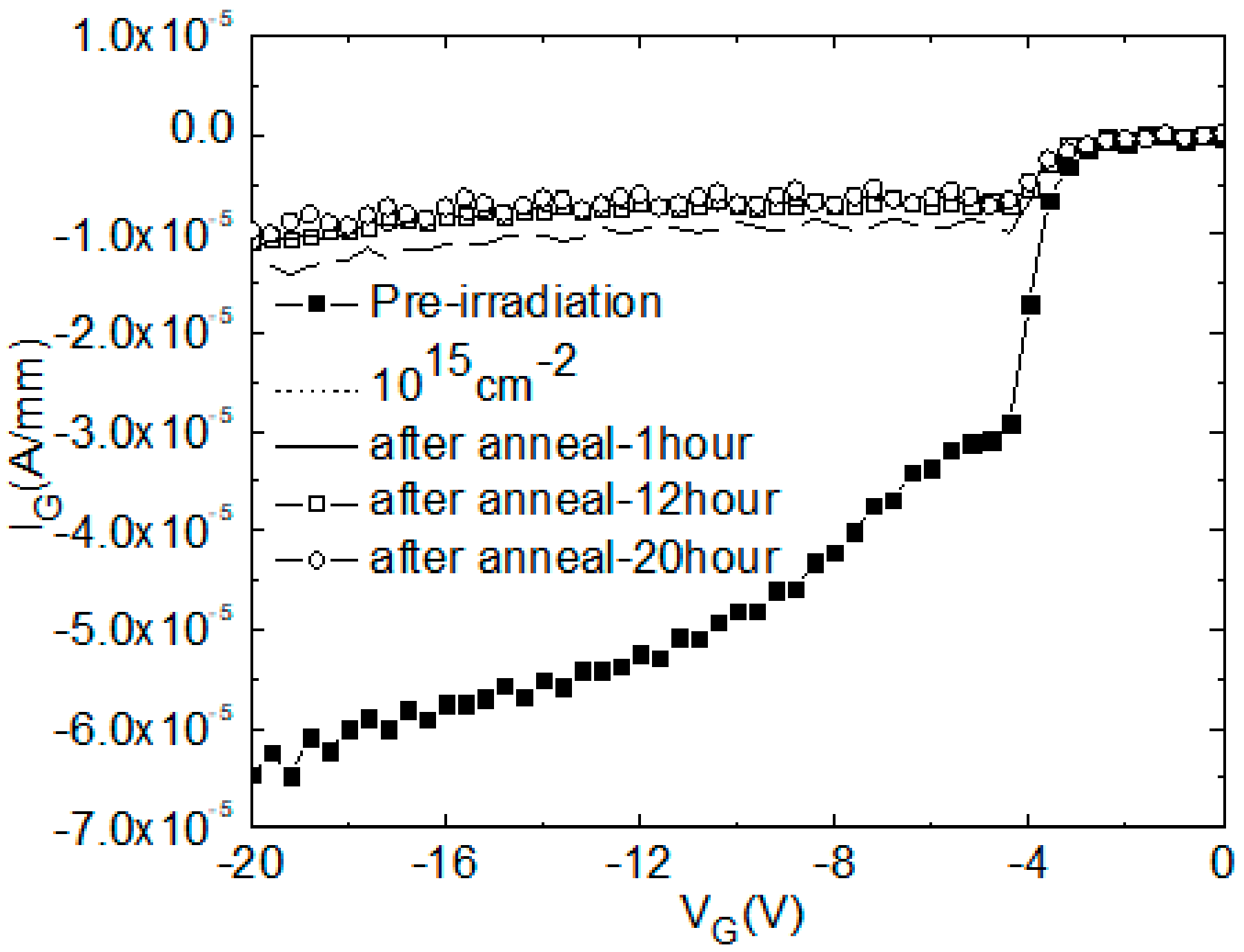
Figure 9.
Transfer characteristics for GaN HEMTs after 60Co γ-ray (a) or proton (b) irradiation and annealing.
Figure 9.
Transfer characteristics for GaN HEMTs after 60Co γ-ray (a) or proton (b) irradiation and annealing.

Table 1.
XRD measurement parameter shifts for GaN heterostructures after 1015 cm−2 neutrons.
| No. | (002) FWHM/arcsec | (102) FWHM/arcsec | ||
|---|---|---|---|---|
| Pre-Irradiation | Post-Irradition | Pre-Irradiation | Post-Irradition | |
| 1 | 588 | 647 | 912 | 1079 |
| 2 | 310 | 311 | 789 | 813 |
Table 2.
The main normalized parameters of AFM after 1015 cm−2 neutrons.
| No. | RMS | ρ | d |
|---|---|---|---|
| 1 | 2.16 | 1.35 | 2.08 |
| 2 | 2.27 | 1.18 | 1.33 |
Table 3.
Hall parameter shifts after 1015 cm−2 neutrons.
| No. | ns/(1013 cm−2) | μ/(cm2·V−1·s−1) | Rsh/(Ω/γ) | |||
|---|---|---|---|---|---|---|
| Pre-Irradiation | Post-Irradition | Pre-Irradiation | Post-Irradition | Pre-Irradiation | Post-Irradition | |
| 1 | 1.68 | 1.45 | 698 | 716 | 519 | 548 |
| 2 | 1.94 | 1.88 | 937 | 951 | 407 | 419 |
© 2018 by the authors. Licensee MDPI, Basel, Switzerland. This article is an open access article distributed under the terms and conditions of the Creative Commons Attribution (CC BY) license (http://creativecommons.org/licenses/by/4.0/).
Share and Cite
MDPI and ACS Style
Gu, W.; Xu, X.; Zhang, L.; Gao, Z.; Hu, X.; Zhang, Z. Study on Neutron Irradiation-Induced Structural Defects of GaN-Based Heterostructures. Crystals 2018, 8, 198. https://doi.org/10.3390/cryst8050198
AMA Style
Gu W, Xu X, Zhang L, Gao Z, Hu X, Zhang Z. Study on Neutron Irradiation-Induced Structural Defects of GaN-Based Heterostructures. Crystals. 2018; 8(5):198. https://doi.org/10.3390/cryst8050198
Chicago/Turabian StyleGu, Wenping, Xiaobo Xu, Lin Zhang, Zhiyuan Gao, Xiaochuan Hu, and Zan Zhang. 2018. "Study on Neutron Irradiation-Induced Structural Defects of GaN-Based Heterostructures" Crystals 8, no. 5: 198. https://doi.org/10.3390/cryst8050198
Note that from the first issue of 2016, this journal uses article numbers instead of page numbers. See further details here.