Article

Inducing Crystallinity of Metal Thin Films with Weak Magnetic Fields without Thermal Annealing

by
Stefan S. Ručman
1,2,
Winita Punyodom
3,4,5,
Jaroon Jakmunee
3 and
Pisith Singjai
4,5,6,7,*
1
Environmental Science Program, Environmental Science Research Center, Faculty of Science, Chiang Mai University, Chiang Mai 50200, Thailand
2
Graduate School, Chiang Mai University 239, Huay Kaew Road, Muang District, Chiang Mai 50200, Thailand
3
Department of Chemistry, Faculty of Science, Chiang Mai University, Chiang Mai 50200, Thailand
4
Materials Science Research Center, Faculty of Science, Chiang Mai University, Chiang Mai 50200, Thailand
5
Center of Excellence in Materials Science and Technology, Chiang Mai University, Chiang Mai 50200, Thailand
6
Department of Physics and Materials Science, Faculty of Science, Chiang Mai University, Chiang Mai 50200, Thailand
7
Center of Excellence in Physics and Astronomy, Faculty of Science, Chiang Mai University, Chiang Mai 50200, Thailand
*
Author to whom correspondence should be addressed.
Crystals 2018, 8(9), 362; https://doi.org/10.3390/cryst8090362
Submission received: 31 May 2018 / Revised: 1 September 2018 / Accepted: 6 September 2018 / Published: 13 September 2018

Abstract

:
Since the discovery of thin films, it has been known that higher crystallinity demands higher temperatures, making the process inadequate for energy-efficient and environmentally friendly methods of thin film fabrication. We resolved this problem by sparking metal wires in a 0.4 Tesla magnetic field at ambient conditions under ultra-pure nitrogen flow to replace the annealing of thin films, and thus designed an environmentally friendly and energy-efficient thin film fabrication method. We employed grazing incidence X-Ray Diffraction spectroscopy to characterize crystallinity of Iron, Nickel, Copper and Tungsten thin films prepared by a sparking discharge process in the presence of 0.4 T magnetic field at an ambient temperature of 25 °C. Control experiment was conducted by sparking without a magnetic field present and using ultra-pure nitrogen flow and ambient air containing oxygen. The Iron thin film prepared in ultra-pure nitrogen flow preserved crystallinity even after one year of ageing. Nickel exhibited higher crystallinity when sparked in nitrogen gas flow than when sparked in atmospheric air and was the only element to crystalize under atmospheric air. Tungsten successfully crystalized after just 40 min of sparking and aluminium failed to crystalize at all, even after 12 h of sparking under nitrogen flow.

Graphical Abstract

1. Introduction

The thinner a thin film is, the higher the thermal conditions required for it to crystalize [1,2,3], therefore, if it is combined with nanocomposite material or deposited on substrate material that is not able to sustain high temperatures, it represents a dead end for scaling up or commercialization [4,5]. In the field of material chemistry, low temperature processing is done at temperatures of 600 °C or less [6]. Currently used strategies for crystallization of thin films in the fabrication of Ti2O thin films are water vapor and UV-induced crystallization [7,8,9]. Research into ambient temperature (syn. Room temperature, 20–45 °C) opens up new possibilities for an approach that can provide a cost-effective synthesis allowing for integration of thin film with temperature sensitive substrates and providing an alternative for widely used thermal annealing.
Heating-free growth and crystallization of perovskite films at room temperature [10], in ambient air, and without the use of thermal annealing was first reported by Dubey et al. who found that exposure of thin film to humid air (40% RH) promoted crystallization. PbI2 is a building block of perovskite and moisture plays an important role in its crystallization [11,12]. Radiofrequency plasma [13] (RF) treatment developed by Osaki et al. was used to crystalize ITO and Ti2O thin films that were prepared on polyethylene terephalate (PET) substrate by Direct Current (DC) magnetron sputtering method [14]. Miniemulsion (ME) technique was used by Gross group to obtain nanocrystalline CuS [15]. In a review of low-temperature crystallization Bretos et al. [16] points out the crystallization process as a limiting step in the low- temperature processing of metal oxide thin film materials. Apart from photochemistry (UV-induced crystallization), authors also discuss the so-called seeding effect and excess metal addition strategies as strategies for achieving crystallization. There is no mention of ambient (room-temperature) reactions and the authors are exclusively focused on wet routes.
Our research group uses thin films for application in photovoltaics, self-cleaning glass coating, anti-dust coating, thermochromic, sensors, antibacterial and hydrophobic coting as well as air purifiers. If crystallinity is needed for any of the applications, thermal annealing is required, and the applied temperature depends on thickness of the film and composition of the material. In this article, we describe a method of electrically discharging five metal wires at breaking voltage regime of voltage-current relation. Time required for crystallization in the presence of a magnetic field is noted and crystallinity of the material is measured by grazing angle XRD. Results are compared with thin film preparation without a magnetic field present.

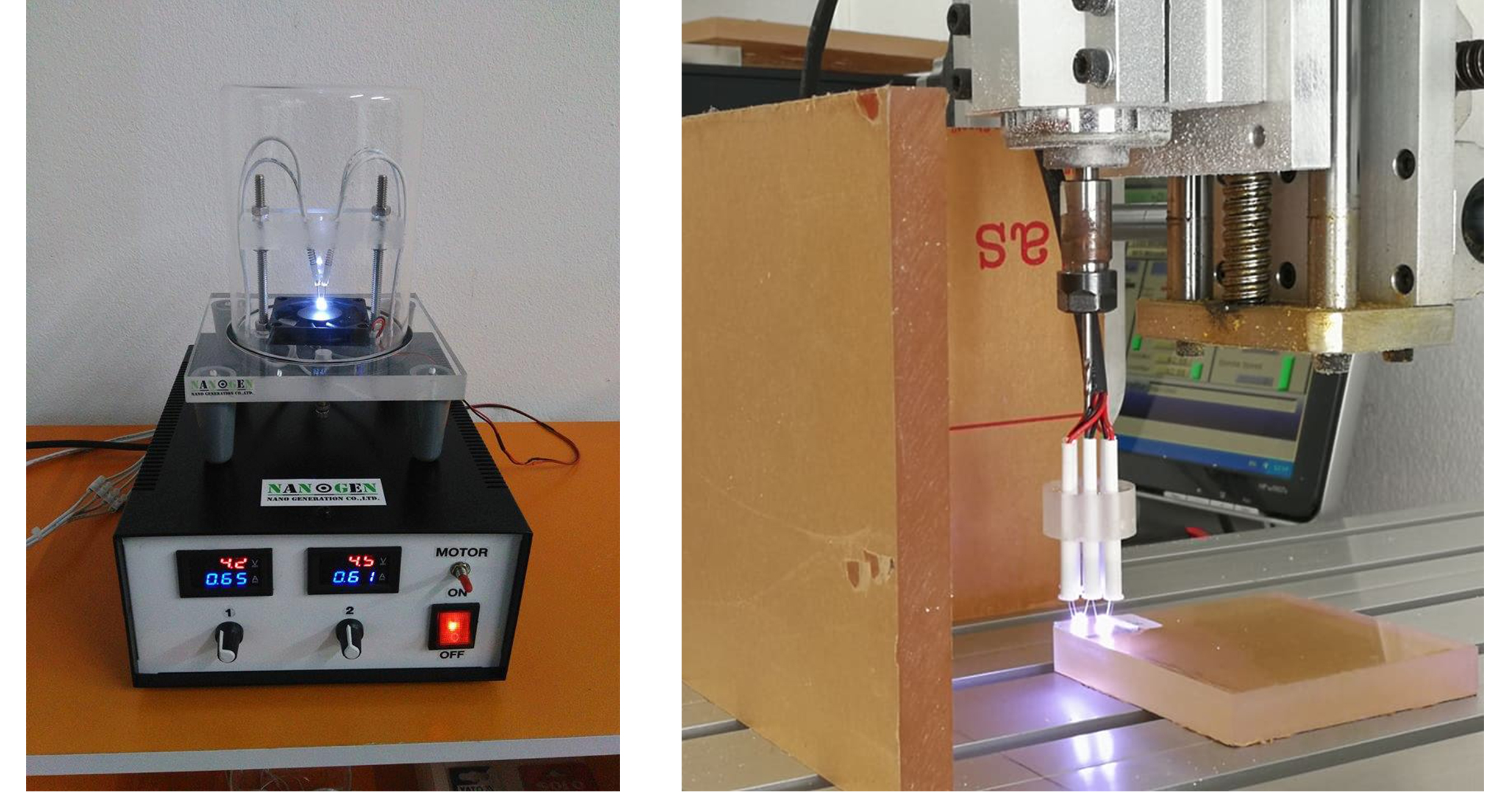
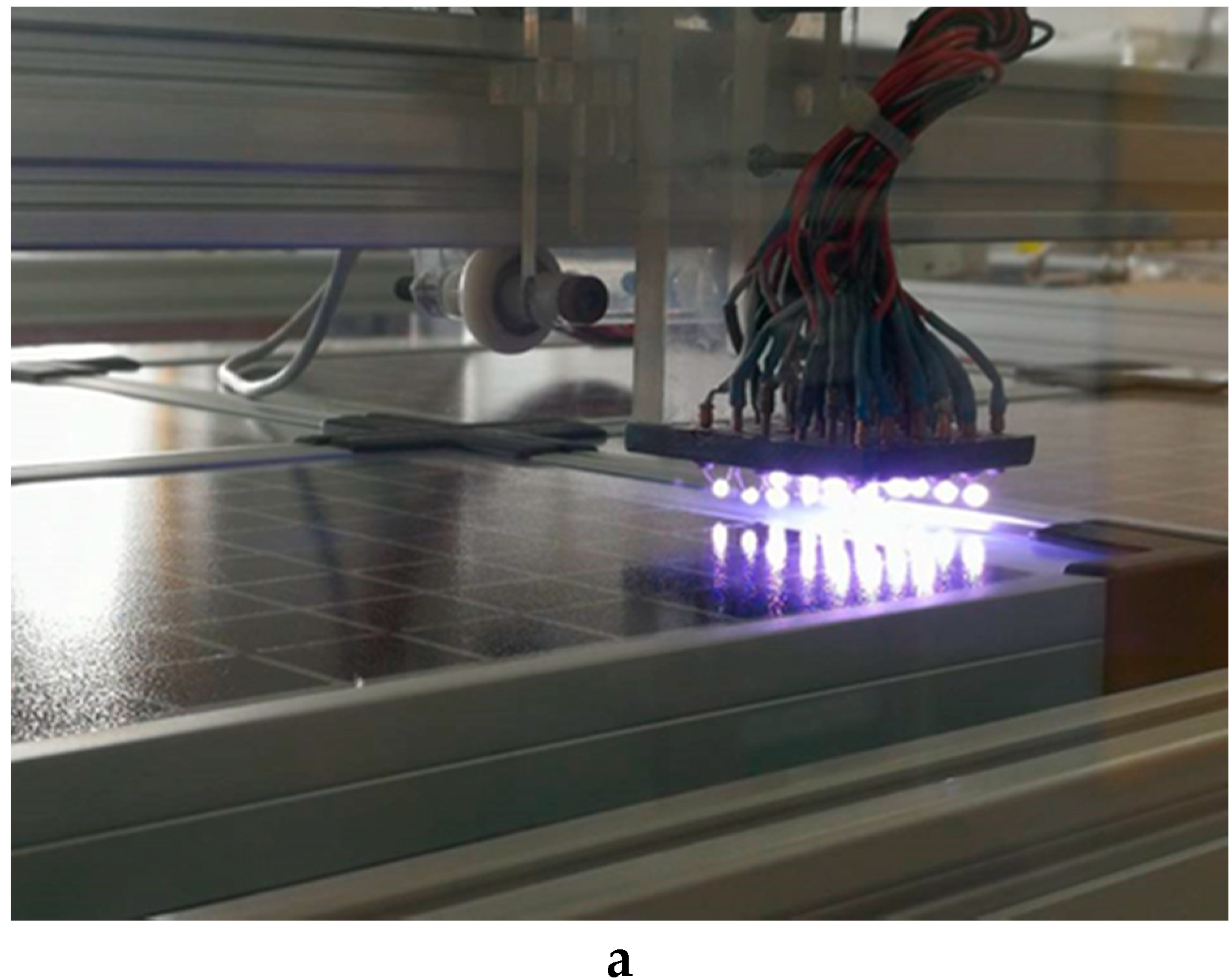
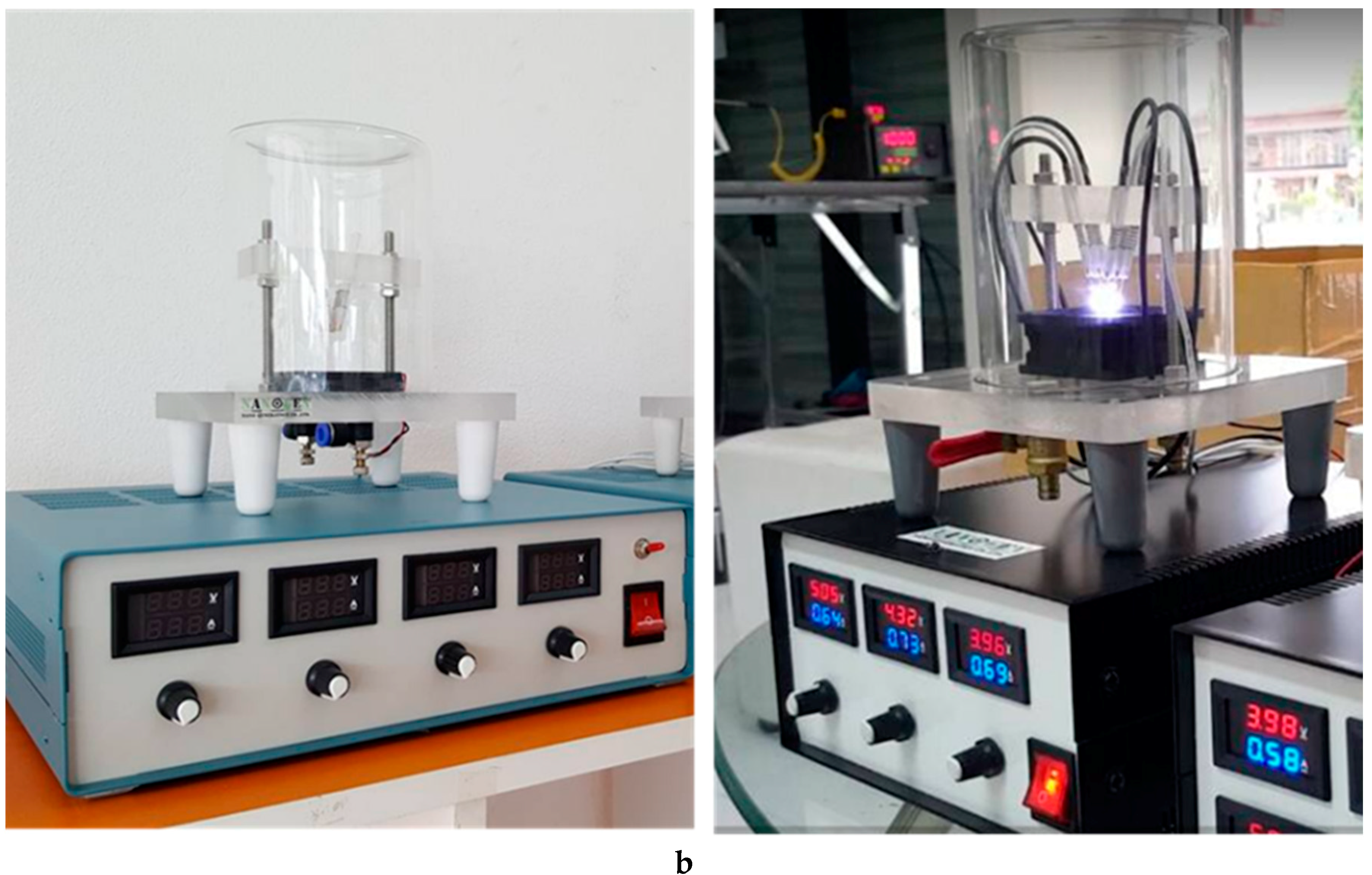
2. Materials and Methods
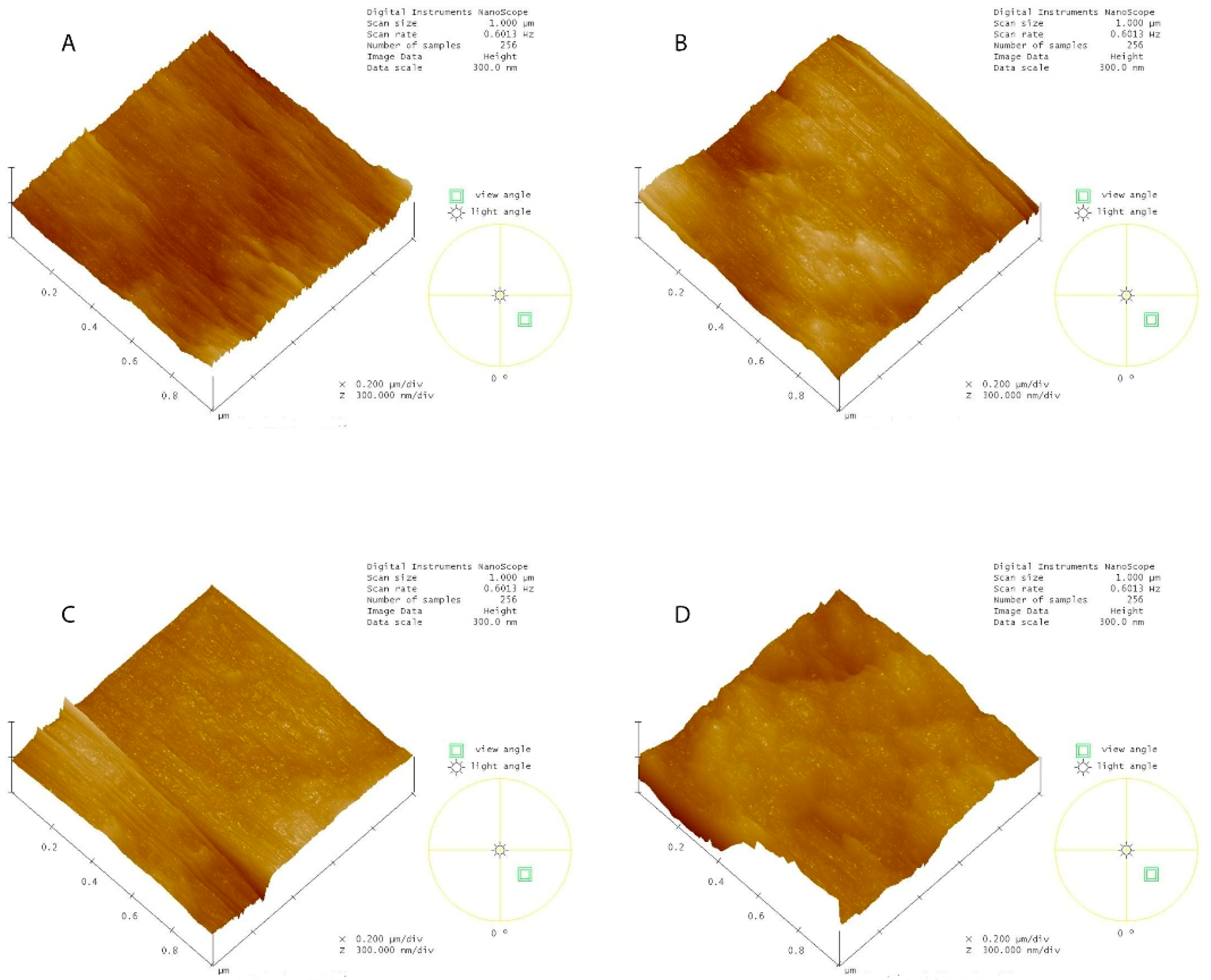
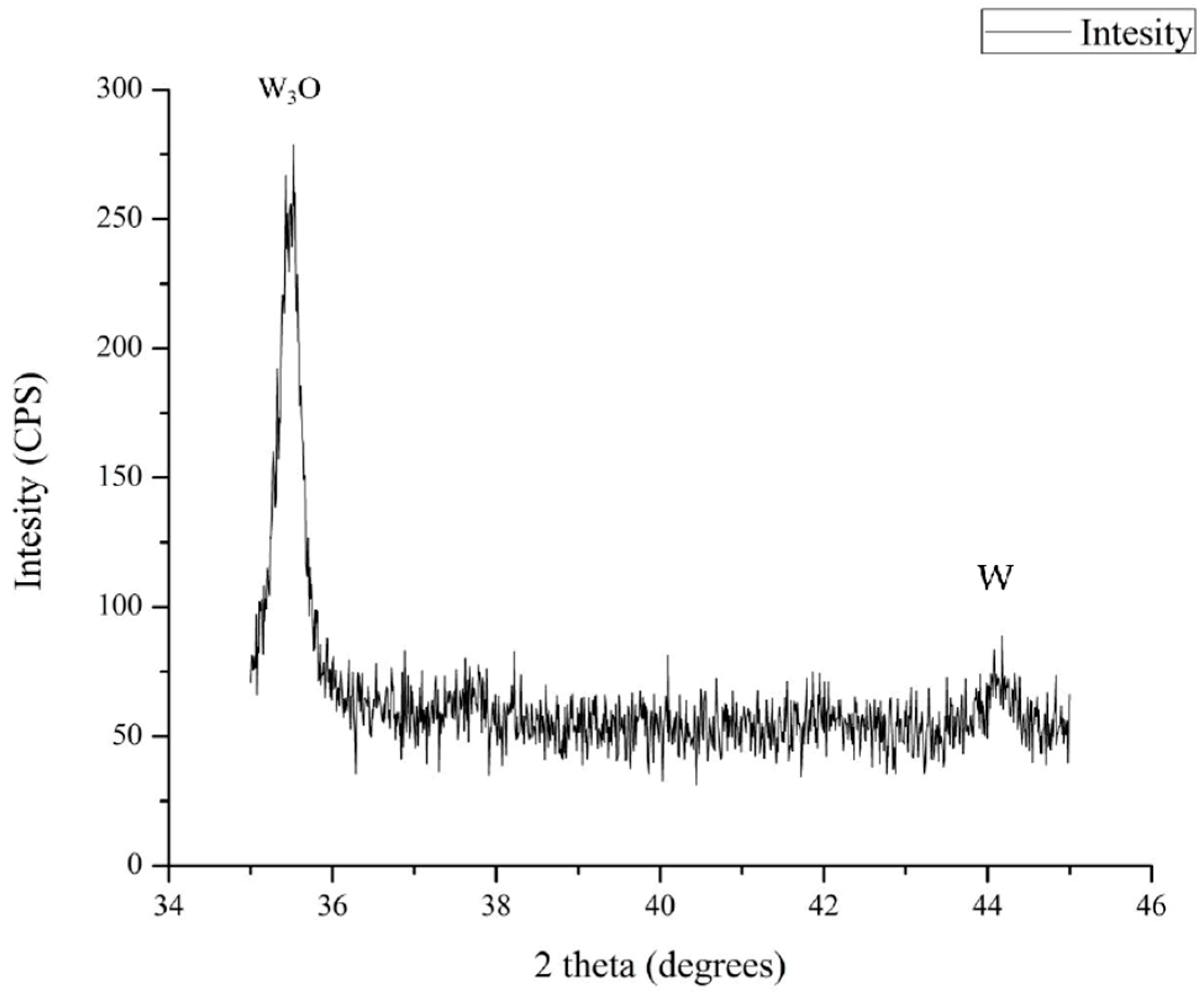
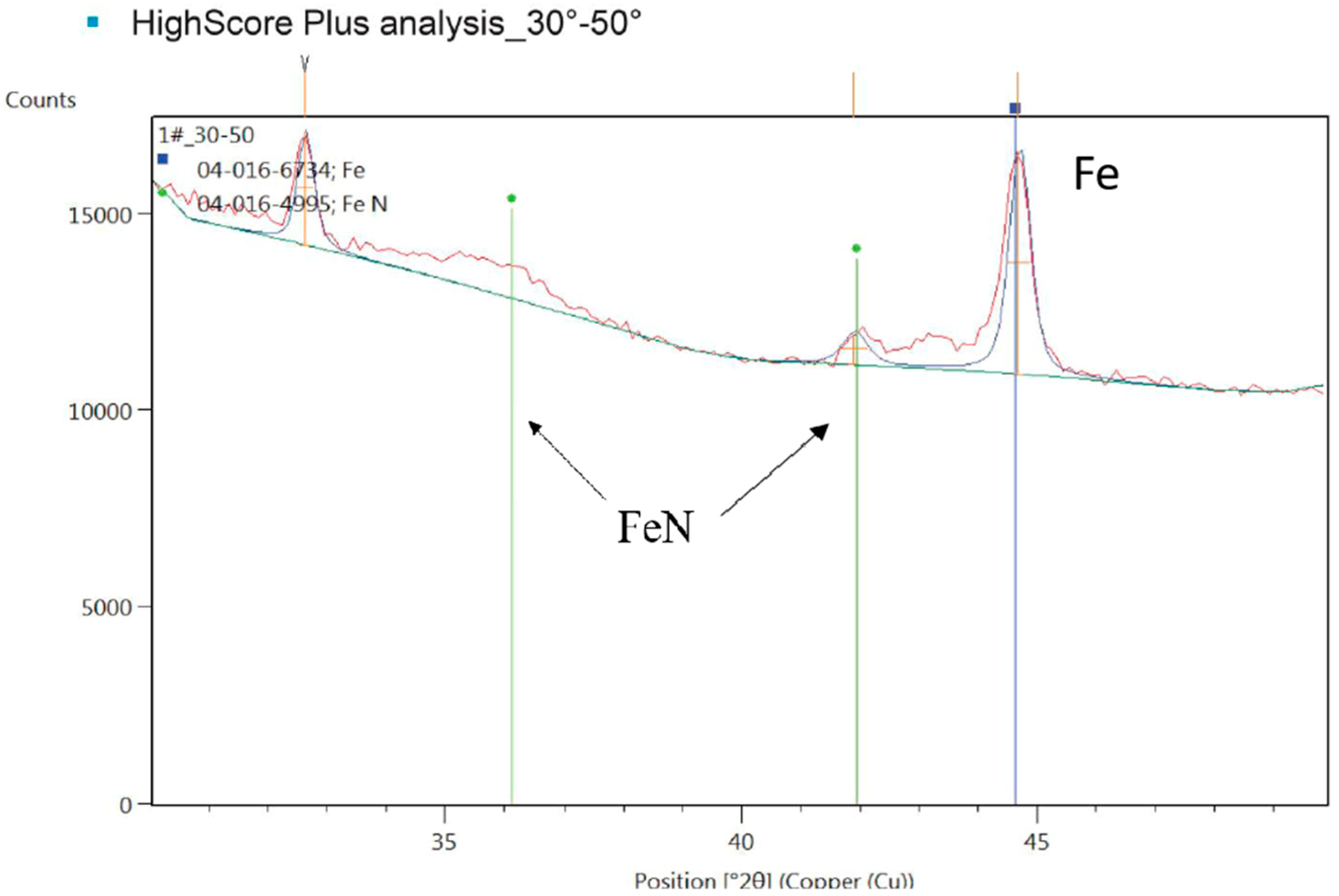
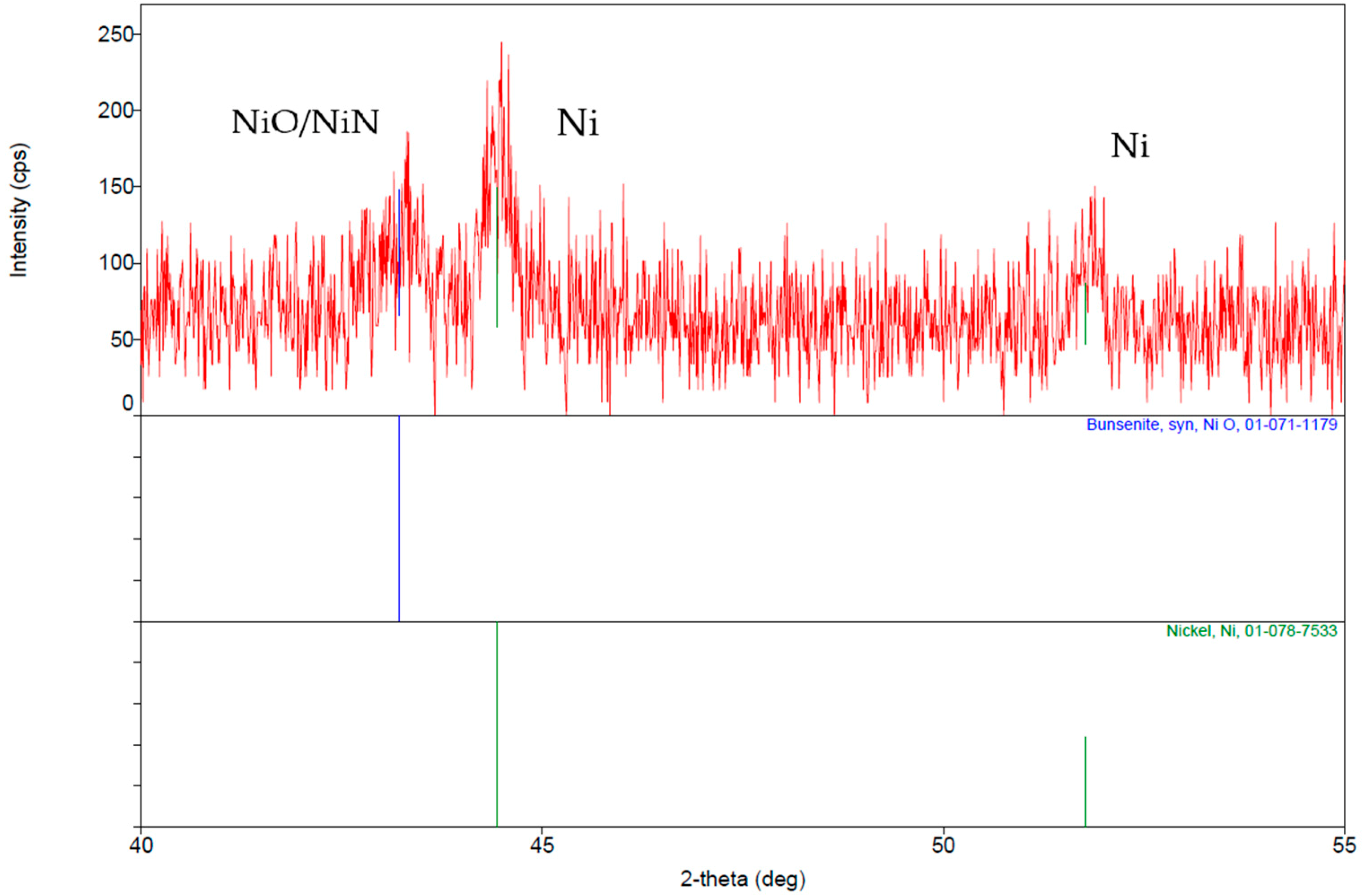
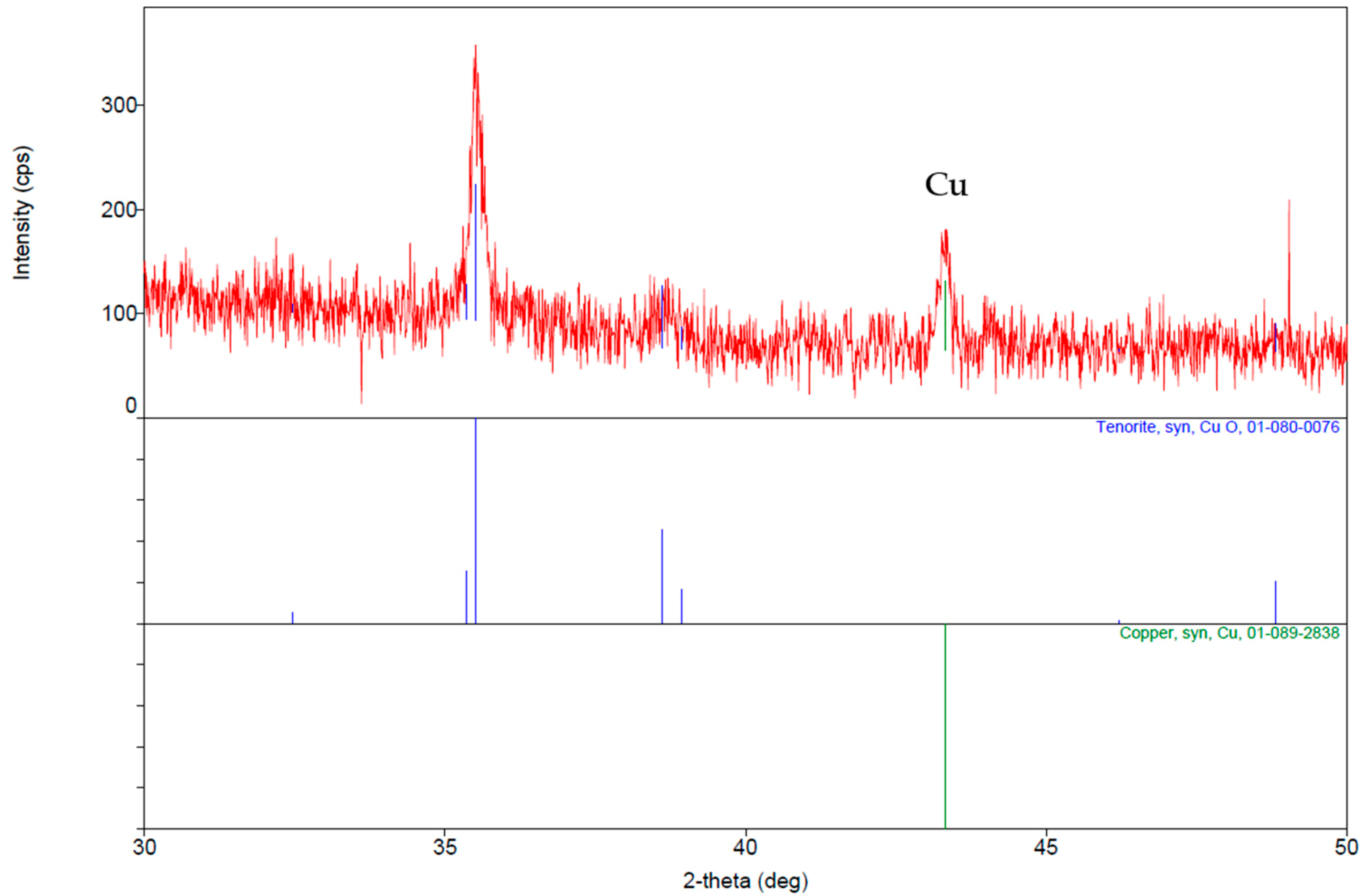
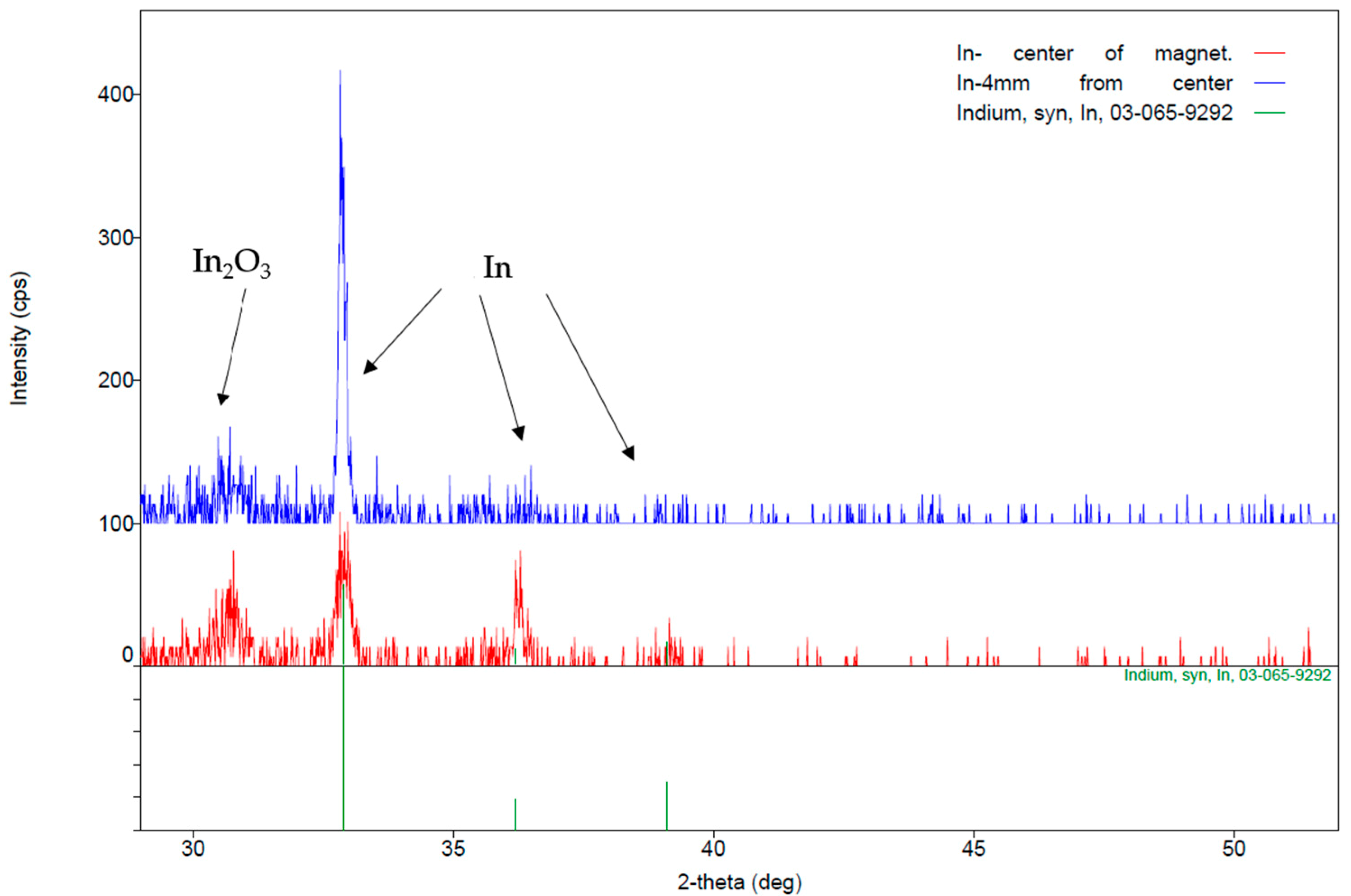
To research crystallization of metal thin films created at room temperature, we employed breaking voltage discharge across tips of metal wires so that the electric current in the gap between wire tips induced ablation, evaporation, and ionization of metal (Al, Fe, Ni, Cu, W). Due to constant discharge, the gap between metal tips, initially set at 2 mm, widens over time because of wire consumption, causing voltage and current applied to it to vary. (4.5 kV ± 0.2%, and 0.6 A ± 0.3%).
Metal wires were purchased from ADVENT (Oxford, UK) research materials, ltd. Iron (FE525711), Aluminium (AL501012), Tungsten (W557609), Copper (CU514511), 99.5% Nickel (NI535311) wire with 0.50 diameter, respectively, and 99.9% Indium wire (IN522109) were annealed in clean conditions. Quartz substrate was used for deposition of nanoparticles onto surface. 0.4 Tesla high temperature Neodymium magnet was obtained from Ningbo Risheng Magnets Co., Ltd. (Ningbo, China). For thin film characterization, Rigaku Smartlab XRD (Rigaku, Tokyo, Japan) with Rigaku’s PDXL software for X-ray analysis was used with Cu source (1.541862 A) and D/teX Ultra 250 detectors.
The sparking discharge method was conducted as follows. Metal nanoparticles were prepared as previously described [17,18,19,20,21,22,23]. Metal wires, purchased from ADVENT, were placed on tips of interchangeable heads in electric circuit, 2 mm apart from each other and 1 mm away from quartz substrate. Circuit elements consisted of a power supply connected to a 7 KV Boost Step-up Power Module High-voltage Generator Transformer (Note: Generator is a commercial name, in scientific context it should be noted that this is a converter) that lead the current to the capacitor, which directed the current to the ends of circuit, modified to hold metallic wires. Two parallel circuits were used, each ending with two interchangeable heads, each head holding a metal wire. Beneath the substrate, a magnet was placed on a rotating motor. Rotation was used to examine how different positions of substrate in the magnetic field influence the crystallinity. Magnetic strength was set at 0.4 T and measured with magnetometer. The ends of the circuit were placed in a flow box where pressure and gas flow were controlled. Nitrogen and atmospheric air flow were used at the rate of 20 L of gas per second.
Ellipsometry machine (J.A Woollam Co., Inc., Lincoln, NE, USA) model α-SETM, with software ComplateEASE Version 3.6, calibrated using SiO2 deposited on pure silicon 250 Å; standard mode was used to measure the thickness of the thin film. Average thin film thickness obtained is presented in Table 1.
We also present results of aging Fe iron thin film for a year by exposing it to atmospheric conditions [17]. HighScore, Plus option from PanAnalytical was used for Iron thin film characterization after one-year exposure [18].
Thin film characterization was done by using an Atomic Force Microscope (Digital Instruments, Inc., Santa Barbara CA, USA) (AFM) in the tapping mode equipped with a standard Si tip and operated at a scan size of 1 × 1 µm2 in air at room temperature. Detailed description of AFM characterization can be found in references [24,25]. where aluminium [25] and zinc [24] wires were sparked, and thin film produced.
Atomic absorption spectroscopy (AAS) was used to determinate total concentration of thin film. Substrates are digested with 5 mL of analytical grade nitric acid and aliquoted to 25 mL with ultrapure DI water, all analysis replicated three times. For aluminium (Al) and tin (Sn) AAS model AAnalyst 100, Perkin Elemer was used, for nickel (Ni), iron (Fe), copper (Cu) determination AAS model PinAAcle 900 F. Results represented at Table 2.

3. Results

Our primary objective was to measure the time needed to achieve crystallization of thin films at 0.4 Tesla. Various metals were used in this study, however, we failed to achieve any crystallization of aluminium under nitrogen, Argon or oxygen-containing flow, respectively. After 12 h of sparking, there were no visible peaks on XRD. However, the texture, morphology and thickness of aluminium thin film was different if deposited in the presence of a magnetic field or without one. Namely, using electron microscopy and AFM, we observed higher porosity of a thin film deposited without a magnetic field, whereas in the presence of a magnetic field, the texture was more compact, and the film was 0.35 microns thick. On the other hand, the thin film deposited without a magnetic field had a thickness of 0.1 micron. Figure 1.
In contrast, Tungsten, a paramagnetic metal, exhibited crystallization after 45 min in ambient atmosphere, corresponding to peak intensity achieved by annealing at 400 degrees as reported previously [26,27].
Figure 2 represents the following two W phases: (a) higher peak W3O (00-041-1230) and (b) smaller peak at 44.2 degrees representing beta W (03-065-6453). The influence of the magnetic field on crystallization of tungsten in ambient conditions for 45 min can be explained intuitively by the mechanism of turning bulk paramagnetic material into superparamagnetic particles by spark discharge, which can cause the nanoparticles produced to become trapped in a magnetic field. Additionally, texture comparison of a thin film prepared without a magnetic field with one prepared in the presence of the magnetic field, showed increased thickness and decreased porosity. These results are in line with the previously reported work on WO3 preparation by spark discharge [26], with and without termal anneling. Since we worked well below W melting and boiling points, oxygen could not be purged from the material, causing contamination, and we can therefore, explain oxidation of W as other authors did. While preparing W and W3O thin films, they observed that a low oxidized tungsten phase existed from the beginning of thin film growth [27] which could not be related to oxygen contamination in the chamber. We can conclude with certainty that no atmospheric oxygen was integrated into the thin film trough vaporization/ionization reaction. Furthermore, higher intensity of W3O compared to pure W is likely related to tungsten target cleaning [28], which was not done in the present experiment. Obtaining pure tungsten thin films requires following specific standards [29] regarding starting material choice, substrate deposition [30], and post-deposition treatment [31].
The integration of oxygen and nitrogen was previously reported [17] in an experiment where zerovalent iron starting material was used. (see Supporting Information S1–S3) Thin films from this experiment preserved crystallinity even after one year of exposure to ambient conditions as represented in Figure 3. The integration of atmospheric nitrogen during the spark discharge process and the correlation of nitrogen integration with the magnetic field strength was published in reference 17 and the underlying mechanism is explained based on the example of a nitrogen laser, exciting gas by breaking voltage. Similarly, the arc-discharge method in nitrogen atmosphere with gold wires as the starting material, successfully synthetized gold-nitride [32].
Another ferromagnetic material we worked with was Nickel, which crystalized after 30 min of sparking. We also explored the possibility for sparked Nickel to incorporate nitrogen. In nitrogen flow, at 0.4 T, the phases we detected were Ni3N (01-070-9598) and a pure zerovalent Nickel phase (03-065-0380). Mixed-phase nickel-based thin films have important applications for water splitting [33] and environmental technologies [34].
Figure 4 represents GIXRD results of Nickel wire sparked in nitrogen flow at 0.4 T. The intensity of XRD peaks decreased if Nickel was ionised at atmospheric air, which is in contrast with Nickel sparked in pure nitrogen. Possible presence of preserved zerovalent Nickel (03-065-2865), NiN (01-083-8042), and NiO (00-047-1049) phases was observed, however, XPS characterization is needed to confirm whether these are oxide or nitride phases. Another issue is that different air flows result in different crystallinity and morphology, which was already observed by Schmid-Otto research group that described how gas flow influences nanoparticle morphology [35].
Copper was the diamagnetic material used for sparking in nitrogen flow at 0.4 T field. Given the material used, the results of XRD analysis of crystallization and the identification of phases with nitrides or oxides were unexpected. It took 30 min for thin film to be fabricated. The phases represented in Figure 5 are pure Cu phase (03-065-9743) and CuN phase (01-076-8854). These phases are present due to the influence of the magnetic field on ions or vaporized zerovalent metal, resulting in a mixture of radicals which can react when they are in close proximity with each other. Radical pairs are formed between Copper and excited nitrogen. Nitrogen is ionized by applying voltage trough a spark gap. Only by examining this system from a viewpoint of valence chemistry, can we attempt to explain the lack of crystallization in aluminium which is also diamagnetic. Appendix A represents valence electrons of materials used in this study. Atom ionization with spark discharge produces a two-valence electron atom that successfully pairs with other atoms in the magnetic field and thus opposes the crystallization.

4. Discussion

Gas reactions influenced by magnetic field can be observed during the magnetic spattering method which is used to increase the density of argon ion plasma. Generally, chemical reactions, such as oxidation and nitridification, are not desirable and were suppressed, and therefore, the effect that a magnetron has on chemical reactions was omitted when describing magnetic field-ordered reactions, even though magnetron is a well-known technique used for thin film preparation [36]. A magnetic field is used in magnetron sputtering because it reduces electron mobility. Electrons generated at the cathode are trapped along the magnetic field lines until they undergo collision, thus the residence time of electrons in the region surrounding the cathode is increased and the presence of the field allows electrons to ionize gas more efficiently. The change of strength of the magnetic field affects the ionization rate of the gasses in the system. (Ar, N2 or O2). Sparking process is an ideal combination of magnetron sputtering and water-free medium for establishing conditions of ionization without solvents and obtaining experimental conditions in which chemical reactions can be influenced by a magnetic field without the use of complex apparatuses that magnetron requires.
We could explain crystallization of thin films in magnetic fields by the effect of ground vs excited states of metals, or by valence electron ordering. However, these two approaches were chosen based on the formation of metal ions in liquids and alloys [37] and the size of atom/ion/molecule effect [38]. Aluminium belongs to the boron group and, therefore, has three electrons in the last orbital with valence configuration ns2np1. Sparking an aluminium wire causes ionization with breakdown voltage and our assumption was that the electron from the p-shell would be lost, leading to positive ionization and, therefore, the inability of the magnetic field to interact with the remaining paired electrons. To prove this hypothesis, we sparked an indium wire in a magnetic field. Contrary to our expectations, we achieved crystallization of indium as showed in Figure 6 We obtained two peaks of different intensity, the first one was measured at the centre of the magnet where magnetic field is homogeneous, and the second 3 mm from the centre. Quality assurance of the process was done by sparking of tin (II) oxide (SnO) and preparation of tungsten (W) that covered the whole substrate as recommended by Rigaku. Thin film was prepared without the presence of the magnetic field, with furnace annealing. There was no crystallization in SnO and W-covered substrates. We obtained crystallization of iron, nickel, copper, indium, and tungsten at 0.4 Tesla. These elements differ in terms of atomic number, density, melting points, atomic orbitals, and magnetic properties. We provided evidence that crystallization is achievable outside of water and that the previous hypothesis of proton transfer is not suitable to explain crystallization induced by a magnetic field.

5. Conclusions

We observed how a magnetic field of 0.4 T affects the deposition time on substrate and the crystallinity of thin film. Sparking in oxygen-containing atmosphere versus ultra-pure nitrogen results in thin-films of different colours.
Application of a magnetic field during the fabrication of inorganic thin films with a sparking discharge process can induce and enhance the crystallinity of films and thus potentially improve their properties. This method proves useful with the numerous possibilities for application and with a simple design for enhancement of crystallinity of thin films. As depicted in Appendix B, the sparking head can be modified to suit different purposes, for instance, application of a magnetic field can make the thermal annealing step unnecessary. Enhanced crystallinity implies longevity prolongation and ease of storage.
Turning to the question of how a magnetic field with low strength can influence crystallization, we found that the magnetic field influences metal vapours and ionized metal wire due to the breakdown voltage of atoms with higher electron density than aluminium. However, the influence of the magnetic field on Sodium and Calcium ions [39] in solution poses a question whether this could be related to the concentration of ions in the medium. Since we used two sparking heads with four aluminium wires total and a high deposition time compared to the thickness of the film, we can conclude that the low concentration will not affect formation of crystals, even after a substantial amount of time and thickness is achieved.
As seen further from Table 2. there is no correlation of XRD signal with concentration of thin films on quartz substrates.
All thin films were prepared at ambient conditions which shows the potential for integration with polymer processing and wearable materials that are sensitive to increased temperature. Furthermore, the process used is a breakthrough in energy-efficient synthesis, elucidating the effects that a magnetic field has on crystal formation as an alternative to the claims by Coey and others [40].
Magnetic forces can induce crystallization and is a valuable strategy for chemical free reactions, together with electric field [41], pressure [42], ultrasound [43] and sonication treatment [44].

Supplementary Materials

The following are available online at https://www.mdpi.com/2073-4352/8/9/362/s1, Figure S1: XPS. First two conditions, thin film samples were tested first with GIXRD, and then after 3 weeks tested with XPS, Figure S2: Supporting information for Table S1. of manuscript, Figure S3: Of Supporting Information Pictures of thin film prepared in sparking chamber, Figure S4: Picture of quartz substrate with indium thin film, blue dot depicted position of center. Graphical representation of 3 GIXRD measurements.

Author Contributions

Conceptualization, S.S.R. and P.S.; Methodology, S.S.R.; Software, W.P.; Validation, S.S.R., W.P.; Formal Analysis, S.S.R. and P.S.; Investigation, S.S.R.; Resources, W.P.; Data Curation, P.S. and J.J.; Writing: Original Draft Preparation, S.R.; Writing: Review and Editing, J.J. and S.R.; Visualization, S.S.R.; Supervision, W.P.; J.J. and P.S.; Project Administration, W.P.; Funding Acquisition, W.P. and P.S.

Funding

This research received no external funding.

Acknowledgments

“We wish to thank Center of Excellence in Materials Science and Technology, Chiang Mai University for financial support” under the administration of Materials Science Research Center, Faculty of Science, Chiang Mai University. Stefan R. would like to thank Emanuele Marini for help and support.

Conflicts of Interest

The authors declare no conflict of interest.

Appendix A

Table A1. Sparked materials in this research, valence electrons.
ElementAtomic NumberValence ElectronsDensity g/cm3Melting Point °C
Al13[Ne] 3s23p12.70660
Fe26[Ar] 3d64s27.861535
Ni28[Ar] 3d84s28.9081453
Cu29[Ar] 3d104s18.961085
In49[Kr] 4d105s25p17.31156.6
Tin oxidemoleculeSn = O6.951630
W74[Xe] 4f145d46s219.253422
Source: National Institute of Standards and Technology; nist.gov.

Appendix B

Figure A1. (a) Picture of sparking head modified for solar cell coating; (b) Two apparatus with four and three sparking heads.
Crystals 08 00362 g0a1aCrystals 08 00362 g0a1b

References

  1. Zhang, Q.M.; Xu, H.; Fang, F.; Cheng, Z.Y.; Xia, F.; You, H. Critical thickness of crystallization and discontinuous change in ferroelectric behavior with thickness in ferroelectric polymer thin films. J. Appl. Phys. 2001, 89, 2613–2616. [Google Scholar] [CrossRef]
  2. Chen, R.Q.; Lu, Q.Q.; Cheng, Q.D.; Ao, L.B.; Zhang, C.Y.; Hou, H.; Liu, Y.M.; Li, D.W.; Yin, D.C. An ignored variable: Solution preparation temperature in protein crystallization. Sci. Rep. 2015, 5, 7797. [Google Scholar] [CrossRef] [PubMed]
  3. Ferri, F.A. Low-temperature metal-induced crystallization of Mn-containing amorphous Ge thin films. J. Non Cryst. Solids 2012, 358, 58–60. [Google Scholar] [CrossRef]
  4. Regula, M.; Ballif, C.; Remškar, M.; Lévy, F. Crystallinity and texture promotion in WS2 thin films. J. Vac. Sci. Technol. A 1997, 15, 2323–2329. [Google Scholar] [CrossRef]
  5. Pellegren, J.P.; Sokalski, V.M. Thickness and interface-dependent crystallization of CoFeB alloy thin films. IEEE Trans. Magn. 2015, 51, 1–3. [Google Scholar] [CrossRef]
  6. Yoon, S.Y.; Kim, K.H.; Kim, C.O.; Oh, J.Y.; Jang, J. Low temperature metal induced crystallization of amorphous silicon using a Ni solution. J. Appl. Phys. 1997, 82, 5865–5867. [Google Scholar] [CrossRef]
  7. JohnáK, A.; ReenaáPhilip, R. Rapid room temperature crystallization of TiO2 nanotubes. CrystEngComm 2017, 19, 1585–1589. [Google Scholar]
  8. Su, J.; Zou, X.; Li, B.; Chen, H.; Li, X.; Yu, Q.; Mi, Q.; Chen, J.S. Accelerated room-temperature crystallization of ultrahigh-surface-area porous anatase titania by storing photogenerated electrons. Chem. Commun. 2017, 53, 1619–1621. [Google Scholar] [CrossRef] [PubMed] [Green Version]
  9. Lamberti, A.; Chiodoni, A.; Shahzad, N.; Bianco, S.; Quaglio, M.; Pirri, C.F. Ultrafast room-temperature crystallization of TiO2 nanotubes exploiting water-vapor treatment. Sci. Rep. 2015, 5, 7808–7814. [Google Scholar] [CrossRef] [PubMed]
  10. Dubey, A.; Kantack, N.; Adhikari, N.; Reza, K.M.; Venkatesan, S.; Kumar, M.; Khatiwada, D.; Darling, S.; Qiao, Q. Room temperature, air crystallized perovskite film for high performance solar cells. J. Mater. Chem. A 2016, 4, 10231–10240. [Google Scholar] [CrossRef]
  11. Ciro, J.; Betancur, R.; Mesa, S.; Jaramillo, F. High performance perovskite solar cells fabricated under high relative humidity conditions. Sol. Energy Mater. Sol. Cells 2017, 163, 38–42. [Google Scholar] [CrossRef]
  12. Kye, Y.H.; Yu, C.J.; Jong, U.G.; Chen, Y.; Walsh, A. Critical role of water in defect aggregation and chemical degradation of perovskite solar cells. J. Phys. Chem. Lett. 2018, 9, 2196–2201. [Google Scholar] [CrossRef] [PubMed]
  13. Ohsaki, H.; Shibayama, Y.; Suzuki, M.; Kinbara, A.; Yashiro, H.; Watanabe, T. Room temperature crystallization by RF plasma. Thin Solid Films 2008, 516, 4490–4494. [Google Scholar] [CrossRef]
  14. Ohsaki, H.; Suzuki, M.; Shibayama, Y.; Kinbara, A.; Watanabe, T. Room temperature crystallization of indium tin oxide films on glass and polyethylene terephthalate substrates using RF plasma. J. Vac. Sci. Technol. A 2007, 25, 1052–1055. [Google Scholar] [CrossRef]
  15. Morgese, G.; Dolcet, P.; Feis, A.; Gellini, C.; Gialanella, S.; Speghini, A.; Badocco, D.; Pastore, P.; Casarin, M.; Gross, S. Room-temperature crystallization of CuS nanostructures for photothermal applications through a nanoreactor approach. Eur. J. Inorg. Chem. 2017, 20, 2745–2754. [Google Scholar] [CrossRef]
  16. Bretos, I.; Jiménez, R.; Ricote, J.; Calzada, M.L. Low-temperature crystallization of solution-derived metal oxide thin films assisted by chemical processes. Chem. Soc. Rev. 2018, 47, 291–308. [Google Scholar] [CrossRef] [PubMed] [Green Version]
  17. Stefan, R.; Jakmunee, J.; Punyodom, W.; Singjai, P. A novel strategy for longevity prolongation of iron-based nanoparticle thin films by applied magnetic force. New J. Chem. 2018, 42, 4807–4810. [Google Scholar]
  18. Maillé, L.; Sant, C.; Le Paven-Thivet, C.; Legrand-Buscema, C.; Garnier, P. Structure and morphological study of nanometer W and W3O thin films. Thin Solid Films 2003, 428, 237–241. [Google Scholar] [CrossRef]
  19. Degen, T.; Sadki, M.; Bron, E.; König, U.; Nénert, G. The highscore suite. Powder Diffr. 2014, 29, S13–S18. [Google Scholar] [CrossRef]
  20. Kumpika, T.; Thongsuwan, W.; Singjai, P. Optical and electrical properties of ZnO nanoparticle thin films deposited on quartz by sparking process. Thin Solid Films 2008, 516, 5640–5644. [Google Scholar] [CrossRef]
  21. Chuminjak, Y.; Daothong, S.; Kuntarug, A.; Phokharatkul, D.; Horprathum, M.; Wisitsoraat, A.; Tuantranont, A.; Jakmunee, J.; Singjai, P. High-performance electrochemical energy storage electrodes based on nickel oxide-coated nickel foam prepared by sparking method. Electrochim. Acta 2017, 238, 298–309. [Google Scholar] [CrossRef]
  22. Chuminjak, Y.; Daothong, S.; Reanpang, P.; Mensing, J.P.; Phokharatkul, D.; Jakmunee, J.; Wisitsoraat, A.; Tuantranont, A.; Singjai, P. Electrochemical energystorage performances of nickel oxide films prepared by a sparking. RSC Adv. 2015, 5, 67795–67802. [Google Scholar] [CrossRef]
  23. Meuller, B.O.; Messing, M.E.; Engberg, D.L.; Jansson, A.M.; Johansson, L.I.; Norlén, S.M.; Tureson, N.; Deppert, K. Review of spark discharge generators for production of nanoparticle aerosols. Aerosol Sci. Technol. 2012, 46, 1256–1270. [Google Scholar] [CrossRef]
  24. Kumpika, T.; Thongsuwan, W.; Singjai, P. Atomic force microscopy imaging of ZnO nanodots deposited on quartz by sparking off different tip shapes. Surf. Interface Anal. 2007, 39, 58–63. [Google Scholar] [CrossRef]
  25. Kumpika, T.; Kantarak, E.; Sroila, W.; Panthawan, A.; Jhuntama, N.; Sanmuangmoon, P.; Thongsuwan, W.; Singjai, P. Superhydrophilic/superhydrophobic surfaces fabricated by spark-coating. Surf. Interface Anal. 2018, 50, 827–834. [Google Scholar] [CrossRef]
  26. Isaac, N.A.; Valenti, M.; Schmidt-Ott, A.; Biskos, G. Characterization of tungsten oxide thin films produced by spark ablation for NO2 gas sensing. ACS Appl. Mater. Interfaces 2016, 8, 3933–3939. [Google Scholar] [CrossRef] [PubMed]
  27. Vernardou, D.; Psifis, K.; Louloudakis, D.; Papadimitropoulos, G.; Davazoglou, D.; Katsarakis, N.; Koudoumas, E. Low pressure CVD of electrochromic WO3 at 400 °C. J. Electrochem. Soc. 2015, 162, H579–H582. [Google Scholar] [CrossRef]
  28. Sun, H.L.; Song, Z.X.; Guo, D.G.; Ma, F.; Xu, K.W. Microstructure and mechanical properties of nanocrystalline tungsten thin films. J. Mater. Sci. Technol. 2010, 26, 87–92. [Google Scholar] [CrossRef]
  29. Zakeri, K.; Peixoto, T.R.F.; Zhang, Y.; Prokop, J.; Kirschner, J. On the preparation of clean tungsten single crystals. Surf. Sci. 2010, 604, L1–L3. [Google Scholar] [CrossRef]
  30. Girault, B.; Eyidi, D.; Goudeau, P.; Sauvage, T.; Guerin, P.; Bourhis, E.L.; Renault, P.O. Controlled nanostructuration of polycrystalline tungsten thin films. J. Appl. Phys. 2013, 113, 174310. [Google Scholar] [CrossRef]
  31. Hao, Q.; Chen, W.; Xiao, G. Beta (β) tungsten thin films: Structure, electron transport, and giant spin Hall effect. Appl. Phys. Lett. 2015, 106, 182403. [Google Scholar] [CrossRef]
  32. Quintero, J.H.; Mariño, A.; Šiller, L.; Restrepo-Parra, E.; Caro-Lopera, F.J. Rocking curves of gold nitride species prepared by arc pulsed-physical assisted plasma vapor deposition. Surf. Coat. Technol. 2017, 309, 249–257. [Google Scholar] [CrossRef]
  33. Shalom, M.; Ressnig, D.; Yang, X.; Clavel, G.; Fellinger, T.P.; Antonietti, M. Nickel nitride as an efficient electrocatalyst for water splitting. J. Mater. Chem. A 2015, 3, 8171–8177. [Google Scholar] [CrossRef] [Green Version]
  34. Rudd, P.A.; Liu, S.; Gagliardi, L.; Young, V.G., Jr.; Lu, C.C. Metal-alane adducts with zero-valent nickel, cobalt, and iron. J. Am. Chem. Soc. 2011, 133, 20724–207273. [Google Scholar] [CrossRef] [PubMed]
  35. Feng, J.; Guo, X.; Ramlawi, N.; Pfeiffer, T.V.; Geutjens, R.; Basak, S.; Nirschl, H.; Biskos, G.; Zandbergen, H.W.; Schmidt-Ott, A. Green manufacturing of metallic nanoparticles: A facile and universal approach to scaling up. J. Mater. Chem. A 2016, 4, 11222–11227. [Google Scholar] [CrossRef]
  36. Swann, S. Magnetron sputtering. Phys. Technol. 1988, 19, 67–75. [Google Scholar] [CrossRef]
  37. Matsuda, T.; Umeda, K.; Kato, Y.; Nishimoto, D.; Furuta, M.; Kimura, M. Raremetal-free high-performance Ga-Sn-O thin film transistor. Sci. Rep. 2017, 7, 44326–44332. [Google Scholar] [CrossRef] [PubMed]
  38. Sudha, C.; Sivanarendiran, R.; Srinivasan, K. Influence of magnetic field on the nucleation rate control of mono paracetamol. Cryst. Res. Technol. 2015, 50, 230–235. [Google Scholar] [CrossRef]
  39. Al Helal, A.; Soames, A.; Gubner, R.; Iglauer, S.; Barifcani, A. Influence of magnetic fields on calcium carbonate scaling in aqueous solutions at 150 °C and 1 bar. J. Colloid Interface Sci. 2018, 509, 472–484. [Google Scholar] [CrossRef] [PubMed]
  40. Chibowski, E.; Szcześ, A. Magnetic water treatment–a review of the latest approaches. Chemosphere 2018, 203, 54–67. [Google Scholar] [CrossRef] [PubMed]
  41. Thongpan, W.; Kumpika, T.; Kantarak, E.; Panthawan, A.; Pooseekheaw, P.; Singjai, P.; Tuantranont, A.; Thongsuwan, W. External-electric-field-enhanced uniformity and deposition rate of a TiO2 film prepared by the sparking process. Ukr. J. Phys. 2018, 63, 531–536. [Google Scholar] [CrossRef]
  42. Liu, X.; Zhuang, K.; Lin, S.; Zhang, Z.; Li, X. Determination of supercooling degree, nucleation and growth rates, and particle size for ice slurry crystallization in vacuum. Crystals 2017, 7, 128. [Google Scholar] [CrossRef]
  43. Kim, H.N.; Suslick, K.S. The effects of ultrasound on crystals: Sonocrystallization and sonofragmentation. Crystals 2018, 8, 280. [Google Scholar] [CrossRef]
  44. Zabihi, F.; Eslamian, M. Effect of the ultrasonic substrate vibration on nucleation and crystallization of PbI2 crystals and thin films. Crystals 2018, 8, 60. [Google Scholar] [CrossRef]
Figure 1. AFM results of Nickel and Copper sparked inside and outside of magnetic field (A) Nickel sparked inside of 0.4 T; (B) Nickel with no magnetic field; (C) Copper sparked inside of field; (D) Copper outside of field.
Crystals 08 00362 g001
Figure 2. Grazing incidence angle X-ray diffraction spectroscopy (GIXRD) results of thin films sparked in 0.4 T magnetic field. W3O also known as betta tungsten. (β-tungsten).
Crystals 08 00362 g002
Figure 3. GIXRD HighScopre Plus PanAnalytical analysis of iron nitride thin films, exposed to air for one year, prepared by sparking method. Blue square represent Iron phase (04-016-6734) and green circle Iron-nitride phase (04-016-4995).
Crystals 08 00362 g003
Figure 4. Nickel GIXRD results, sparked in nitrogen for 30 min at 0.4 T magnetic field. Bunsenite (NiO) phase coincidence with nitride phase of Nickel (Ni3N (01-070-9598)). Without magnetic field there is no detectable peak. High background noise is due to copper source used in XRD and low concertation of thin film on substrate.
Crystals 08 00362 g004
Figure 5. Copper wire sparked in nitrogen flow. GIXRD results of Cu thin films prepared under 0.4 T. Amorphous thin films prepared by sparking discharge under no magnetic films are omitted. (CuO and CuN phase coincidence in diffraction peaks).
Crystals 08 00362 g005
Figure 6. Indium wire sparked in nitrogen flow, at 0.4 T. Blue-GIXRD results from centre, Red-4 mm from centre, as depicted at Figure S4.
Crystals 08 00362 g006
Table 1. Average Thickness of thin film prepared by spark discharge, in this study. Measured by ellipsometry.
Thin FilmTime of DepositionThickness (nm ± SD)Roughness (nm ± SD)
Aluminum12 h530 ± 14.0716.41 ± 1.691
Nickel 130 min164.87 ± 27.433.35 ± 5.0
Indium30 min137 ± 1.7914.32 ± 3.12
Copper30 min274.5 ± 2.01210.6 ± 0.39
Tungsten45 min438.9 ± 23.221.4 ± 2.3
Tungsten 245 min618.2 ± 20.33.85 ± 0.3
Tin oxide (SnO)45 min294.7 ± 31.29.5 ± 0.2
Iron 145 min364.7 ± 2.3510 ± 0.5
1 refer to the thin films prepared in oxygen environment; 2 refer to thin film prepared with different method.
Table 2. Average Concentration of metals in thin film prepared by spark discharge, measured by AAS and calculated concentration to fit area of thin film.
ElementMagnetic FieldConcentration (mg/L)Concentration mg/cm2Variation (%)
Al0.4 T9.1590.2291.497
Sn0.4 T10.4270.2612.25
Ni0 T0.8460.0210.72
Ni0.4 T0.3710.0470.83
Fe0 T0.5020.0130.36
Fe0.2 T0.6950.0870.51
Fe0.4 T0.5640.0140.88
Cu0 T1.0160.0260.18
Cu0.4 T1.0050.0250.39

