1. Introduction
In recent days, one of the most important issue in spintronics is to study the magneto-transport phenomenon in magnetic nanostructures. Magnetic nanoparticles have attracted great attention owing to the interaction between the electrical charging effect and spin-dependent tunneling [
1,
2,
3]. These magnetic nanoparticles can be deposited onto insulating substrates, where nanometer-sized magnetic metal particles were confined in the films, and are responsible for giant magnetoresistance (MR).
Furthermore, long distance spin transport properties were observed in chemical vapor deposition (CVD)-grown graphene channels (up to 300 K) [
4,
5,
6]. Different allotropes of carbon might contain distinctive bonding configurations and the hybridization is mainly dependent on the four valance electron orbitals. The four-fold symmetry C(
sp3) hybridization and three-fold symmetry C(
sp2) hybridization, like in diamond and graphite, are two major allotropes [
7]. Amorphous carbon films consist of both
sp2 and
sp3 hybridized carbon atoms in variable proportions.
Growth technique and conditions strongly effect the proportion of C(
sp2) to C(
sp3). For temperature dependence of the conductivity, disorder is considered as a foremost factor in amorphous carbon (a-Carbon) [
8,
9]. Tuning the disorder might make the continuous transition from extended state to localized state possible. External parameters and dopants can change the electronic and physical properties of the carbon-based materials [
10,
11].
In Co–Al–O nanoparticles, enhanced spin accumulation was investigated. The results clearly showed that the spin injection and accretion are considered significant factors, which can support a variety of concepts in spintronics devices [
12]. However, as a result of the interaction of spin with electron motion, the state of spin can change, which may lead to damage of data in spintronics devices [
13]. Regarding the spintronics technology, the integration of multilayer ferromagnetic electrode functional devices is considered a big achievement towards attaining vigorous and accessible tunneling MR. Therefore, the doping of ferromagnetic metal particles in carbon might produce an interesting property in this aspect [
14].
Moreover, graphene is considered as an ideal foundation for the spin transport properties. Owing to such impulsive properties, graphene can be a material for next generation planner spintronics devices [
15]. However, the spin–orbit interactions are weak in carbon, which brings the material to an ideal position to transfer the spin information over a prolonged distance. Carbon has the ability to form a numerous variety of disordered and polycrystalline structures [
16,
17,
18]. We can observe a strong correlation of carbon structure with deposition techniques, and the electronic properties are distinctive for dissimilar structures [
19,
20].
The magnetoresistance usually signifies a phenomenon wherein changes in electrical resistance occur [
21]. Referring to the semiconductor medium for different transport processes, magnetic field-dependent resistance is readily observable in spin-polarized charge injection for the spin-up polarization and spin-down polarization. It is clear from the electroluminescence research, however, that applying an external magnetic field may change the electrical injection current, which is found in single-layer organic light-emitting diodes (OLEDs). The double layer design, having different electrode materials, helped us to confirm the magnetic phenomenon, and was given the name organic magnetoresistance [
22].
Many reports are available on the transport and structural properties of amorphous carbon films doped with Ni, Co, and Fe [
23], but still for the further study of pure a-Carbon systems, we need to investigate these properties. Studies of these a-Carbon films are very important to investigate the effect of amorphous behavior of these materials above their magneto transport properties [
24,
25]. Numerous mechanisms such as wave function shrinkage, grain boundary scattering, diffused scattering at edges, and weak localization [
24,
26], among others, were adopted to study the transport properties of a-Carbon. However, these assumptions are still incapable of giving a proper and clear clarification of the foundation of transport belongings. Therefore, it is very important to proceed with our research on further understanding and investigating the origin of MR for a-Carbon.
In the current study, disordered amorphous carbon films were synthesized with the help of the chemical vapor deposition (CVD) technique. We have further investigated and studied the structural investigation through Raman and X-ray photospectroscopy (XPS), as well as its effect on MR. Non-linear to linear MR curves’ stretching is studied with the change in measurement temperature from a low temperature of 2 K to a higher temperature of 300 K. On selecting different temperature regimes, we investigated the MR mechanisms.
3. Results and Discussion
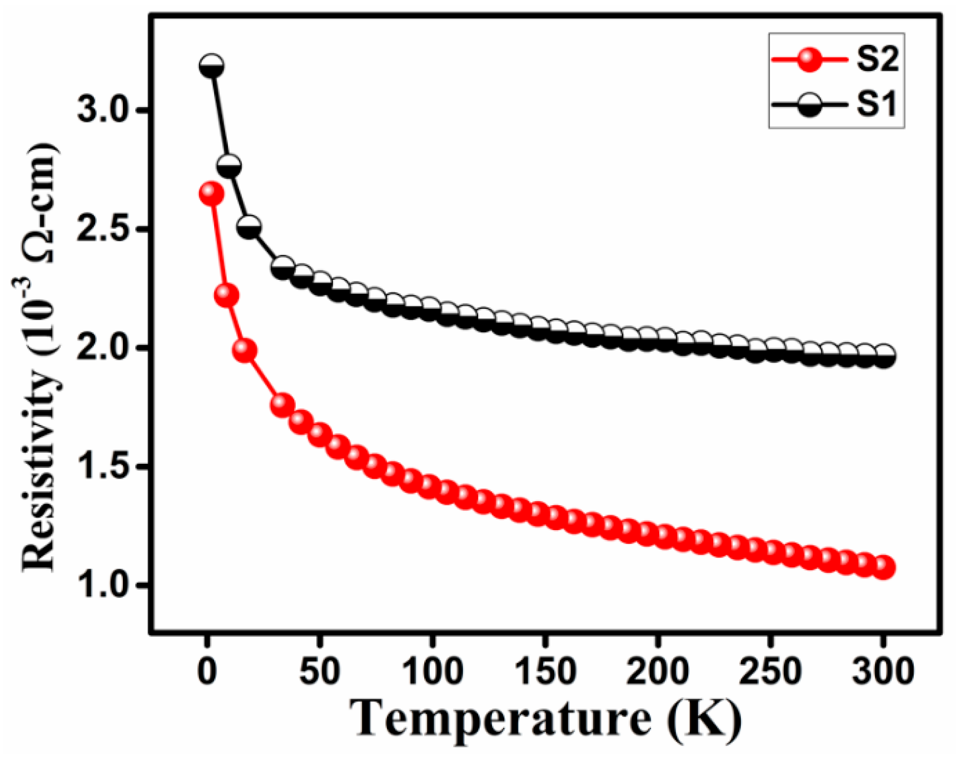
Magnetoresistance is a very complex tool, which probes the scattering process in disordered amorphous structures and is greatly dependent on the temperature dependence of conductivity [
27]. These CVD-grown amorphous carbon film samples lead to the origination of the negative MR phenomenon. Negative MR of both the reported samples was decreased as the temperature was elevated from lower values to room temperature, as shown in
Figure 1. The inset of
Figure 1 shows the schematic of the four-probe sample resistance measurement used for current studies. The MR is defined as [(R
H − R
0)]/R
0], where R
H and R
0 are the resistances with and without a magnetic field, respectively, and the magnetic field direction (“n”) was normal to current (“I”) flowing in the specimen (shown in inset of
Figure 1). The appearance of the two slopes in
Figure 1 for both samples divides the MR change into two regimes with respect to temperature: the lower temperature range (2–50 K) and the higher temperature range (100–300 K). The slope of MR was abrupt for the 2–50 K range, while that of the 100–300 K range was nearly linear. Sample S2 showed a change in negative MR from ~8.2% at 2 K to ~0.5% magnitude at 300 K under the magnetic field of 7 T.
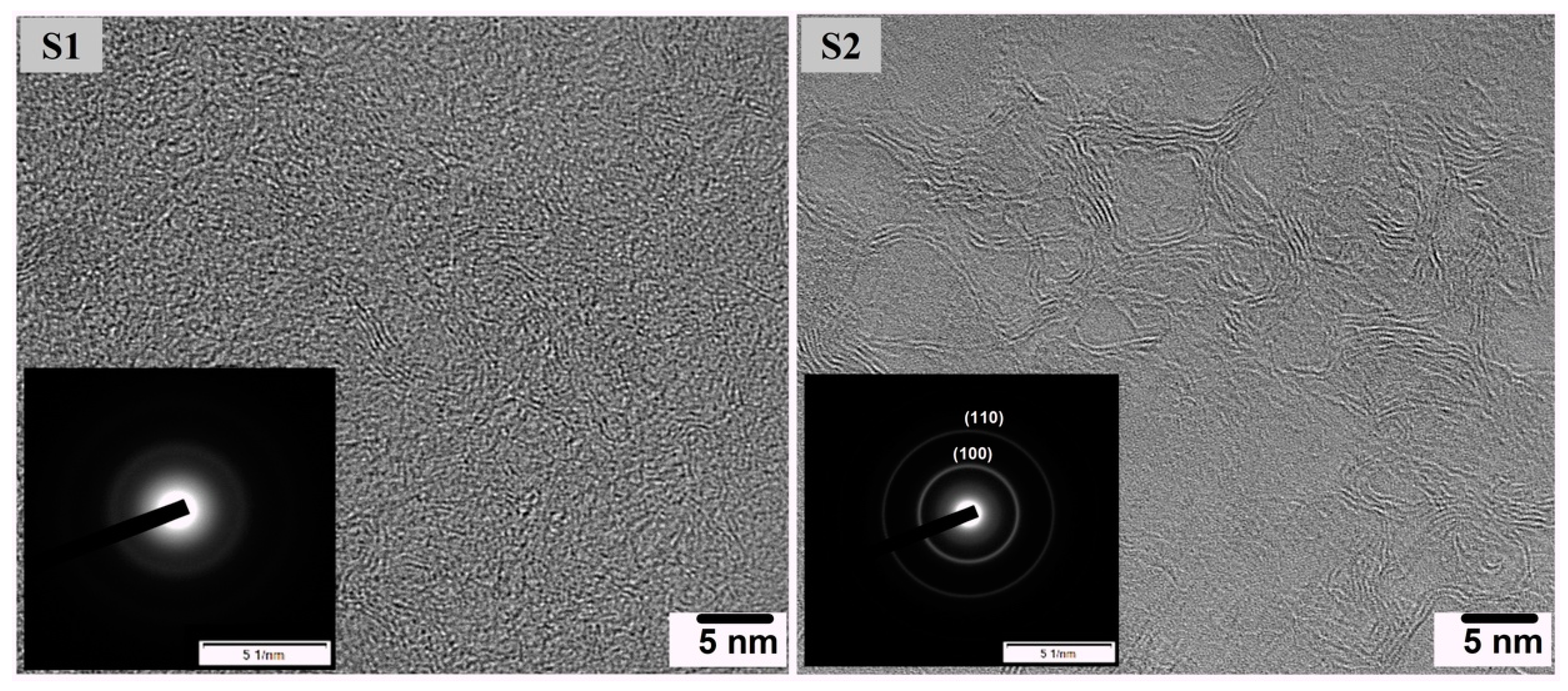
HRTEM was done for insight into morphological investigation of the synthesized amorphous carbon specimens and is shown in
Figure 2. An amorphous-like structure was observed for both samples (S1 and S2), which is also realistic after the diffraction pattern of the inset as illustrated in
Figure 2. In specimen S2, the values of the lattice d-spacing of crystals were recorded as ~0.12 nm and ~0.21 nm, corresponding to the (110) and (100) planes, respectively. The degree of ordered arrangement was much higher in S2 in comparison with S1, which confirmed tremendous oriented graphitic assembly in S2.
The thickness of the samples was observed as 48 nm and 64 nm for samples S1 and S2, respectively. XPS spectra of the thin film sample S1 are shown in
Figure 3 below and the Lorentzian fitting function was used to estimate the exact position of C(
sp2) and C(
sp3) orbitals, which were at ~284.6 eV and ~286.3 eV, respectively.
XPS was then employed for the estimation of the atomic percentage of C(
sp2) and C(
sp3) for both S1 and S2 samples. C(
sp2) of ~78% and C(
sp3) ~22% were estimated for S1, while ~83% and 17% were observed for S2, respectively. Sample S2 showed a larger percentage of C(
sp2), which can be an indication of an increase in conduction as compared with S1. Sample S2 has a more oriented graphitic-like structure, as also shown in
Figure 2. The atomic percentage of C(
sp3) has an inverse relation with C(
sp2) percentage. The atomic percentage ratio of C(
sp2)/C(
sp3) has a direct relation with the structural order of sample S1 and S2.
Those carbon materials that have dominant C(
sp2) clusters are found to be better conductor materials and, on the contrary, those having C(
sp3) clusters are insulators [
28]. The C(
sp2)/C(
sp3) ratio gives a better estimation conduction, which shows that sample S2 possess high conductivity. XPS studies confirmed how these structural parameters might be justified by the conduction phenomenon, which could be responsible for the observed properties of the MR in these amorphous carbon thin films. The lower magnitude of resistivity is observed for the sample S2 with higher structural order. The similar effect of a decrease in resistivity with an increase in measuring temperature from 2 K to 300 K was observed for both samples, as shown in
Figure 4. The maximum magnitude of negative MR is observed for sample S2, having a well-ordered structure with low resistivity. The structural disorder is mainly responsible for the MR properties of these samples.
Figure 5 shows the Raman spectra of different ordered structured samples S1 and S2. Two significant peaks were observed, which were related to Raman D and G modes and the full width at half maximum (FWHM), and the peak shift was estimated for structural information. For samples S1 and S2, the peak shifts of D-band and G-band were found to be within ~1331 cm
−1 to ~1334 cm
−1 and ~1570 cm
−1 to ~1575 cm
−1, respectively. For the samples S1 and S2, the FWHM of the D-band started decreasing from ~137 cm
−1 to ~128 cm
−1 and the FWHM of the G-band started increasing from ~80 cm
−1 to ~85 cm
−1, respectively. As the D-band is related to
A1g (breathing mode of symmetry in six atoms ring of carbon), it is dependent on the defects for activation [
7,
29]. In the maximum disordered structure specimen, the D-band will be more dominant. The intensity of the D-band peak is represented by I
D and the intensity of the G-band peak is denoted by I
G. The degree of disorder (i.e., I
D/I
G) ratio decreases as the C(
sp2) atomic percentage starts increasing up to 83%. Meanwhile, there is direct relation between the FWHM of the D-band and the C(
sp2) atomic %.
The decrease in structural disorder is designated with the decrease in the magnitude of the FWHM of the D-band peak. Meanwhile, the increase in the FWHM of the G-peak leads to the graphitic-like structure. However, the FWHM value of ~128 cm−1 for sample S2 shows a low degree of disorder. Hence, the FWHM value is dependent on the structural disorder. Additionally, the decreasing value from 1.67 to 1.50 of the ratio ID/IG for sample S1 to S2 might give the approximation of the transition from disordered to ordered structure. Thus, for the amorphous carbon materials system, the reduction in the FWHM value and the shift of the D-band peak position of the D-band might present a good approximation for the structural changes, and MR is dependent on these structural parameters for these amorphous carbon samples.
Figure 6 shows the negative MR versus B curves for samples S1 and S2, which were measured in the temperature range of 2–300 K in the magnetic field range of −7 T to 7 T. As the temperature increases, the negative MR value decreases. As the measurement temperature increases from 2 K to 300 K, the shape of the negative MR–B curve shifts from a cone-like shape to a parabolic-like shape. As 10 K was observed as the shifting temperature, non-linear to linear MR was observed, which leads to a significant phenomenon to realize the MR mechanism.
In the current studies, we explored the shift of MR from non-linear to linear MR with respect to the change in measurement temperature.
Figure 4 and
Figure 7 express the resistivity and negative MR measurements’ behavior. It is observed that, for a lower temperature regime (i.e., 2–5 K), the negative non-linear field dependence of MR was observed. Surprisingly, however, for a higher temperature regime (i.e., 20–300 K), linear field dependent MR was observed. Meanwhile, 10 K is noted as the switching temperature from non-linear to linear MR.
Figure 7 explains the field dependent negative MR for different temperatures ranging from 2 K to 300 K. We observed non-linear MR at a lower temperature and, with an increasing temperature after 10 K, the clearly linear negative MR is observed. For both of the samples, the negative MR sharply decreases with the increase in measuring temperature. The same scenario of negative MR was investigated for both of the samples.
At a lower temperature, the difference in the carrier conduction belonging to the quantum interference is responsible for weak localization (WL) and the magnetic field might break the time reversal symmetry. This will result in the decrease of the resistance of the system by affecting the interference. Furthermore, the magnetic field effect possesses the same behavior for inelastic scattering [
26]. Another possible mechanism of negative MR is the diffused scattering (DS), which can be observed at crystallite boundaries of highly disordered materials [
25]. At the grain boundaries, the existence of the crystallites inside the amorphous carbon specimens reveals the scattering spectacle, which shows variation for different temperature ranges depending on the size of the cluster grains for different samples.
We observed variation of negative MR by changing the structural properties. Two negative MR regions were investigated in these samples (i.e., linear MR and non-linear MR). Different mechanism of MR can be related to these different regions for such specimens. This negative MR originated from the diffused scattering at crystallite boundaries and the weak localization. The electrons’ scattering is diffused at the crystallite boundaries for most of the conducting materials. Furthermore, if one of the dimensions of any crystallite is in the nanometer range or about 10 nm, this leads to enriching of the grain boundaries. Then, this diffused scattering becomes the predominant process that will influence the mean free path of the conduction electrons. These small crystallites are more influenced by the magnetic field, which causes an enlargement of the mean free path. As a result, the negative MR is observed. The MR attributable to the diffused scattering is defined in the work of [
30].
where
denotes the mean free path of the carrier exclusive of magnetic field,
is the increment of the mean free path, and
is a constant. We can see the negative MR effect even at a lower temperature i.e., 2–300 K, and this effect decreases sharply with the increases in temperature (also shown in
Figure 1).
Referring to abovementioned argument on the amorphous carbon conduction mechanism, the presence of randomly oriented nano-sized graphitic crystals can be associated with a disordered electronic system. In the disordered systems, the negative MR might instigate after a multiplicity of mechanisms. However, negative MR is the result of the weak localization at a low temperature effect, because, as a result of electron–electron or electron–phonon interaction, the inelastic scattering process affects the phase incoherence between carrier waves, which reduces at high temperatures [
30,
31]. Suppression in backscattered waves coherence as the magnetic field is applied, that is, the weak localization turns out to be weak and negative MR is detected. According to the above discussion, the negative MR of such amorphous carbon specimens might be expressed as
From the aforementioned discussion, we may realize the mechanism of disorder dependence of MR in amorphous carbon films. As compared with ordinary MR, diffused scattering and weak localization effect cause the negative MR at the boundaries of the crystallites. Therefore, the MR increases with the increase in the structural order of the thin films. At lower temperatures (i.e., T < 10 K), the non-linear field dependent negative MR was witnessed, however, it was observed that at higher temperatures, the negative MR was super-linear.


