A Water-Stable Organic-Inorganic Hybrid Perovskite for Solar Cells by Inorganic Passivation


Department of Materials Science & Engineering, McMaster University, 1280 Main St W, Hamilton, ON L8S4L8, Canada
*
Author to whom correspondence should be addressed.
Crystals 2019, 9(2), 83; https://doi.org/10.3390/cryst9020083
Submission received: 17 January 2019
/
Revised: 27 January 2019
/
Accepted: 2 February 2019
/
Published: 4 February 2019
(This article belongs to the Special Issue Advances in Thin Film Solar Cells)
Abstract
:Organic-inorganic hybrid halide perovskite solar cells (PSCs) have been a trending topic in recent years. Significant progress has been made to increase their power conversion efficiency (PCE) to more than 20%. However, the poor stability of PSCs in both working and non-working conditions results in rapid degradation through multiple environmental erosions such as water, heat, and UV light. Attempts have been made to resolve the rapid-degradation problems, including formula changes, transport layer improvements, and encapsulations, but none of these have effectively resolved the dilemma. This paper reports our findings on adding inorganic films as surface-passivation layers on top of the hybrid perovskite materials, which not only enhance stability by eliminating weak sites but also prevent water penetration by using a water-stable layer. The surface-passivated hybrid perovskite layer indicates a slight increase of bandgap energy (Eg = 1.76 eV), compared to the original methylammonium lead iodide (MAPbI3, Eg = 1.61 eV) layer, allowing for more stable perovskite layer with a small sacrifice in the photoluminescence property, which represents a lower charge diffusion rate and higher bandgap energy. Our finding offers an alternative approach to resolving the low stability issue for PSC fabrication.
1. Introduction
Organic perovskite material, methylammonium lead iodide (MAPbI3), reported by Miyasaka et al. [1] in 2009, was first introduced as a dye material in the dye-sensitized solar cell (DSSC) with a mere 3.8% power conversion efficiency (PCE). The PCE has reached over 20% in layer-constructed perovskite solar cells (PSCs), approaching the PCE of 26.7% for single-junction crystalline silicon solar cells [2] by the end of 2017. Although silicon-based solar cells have higher efficiency and much longer lifetime compared to PSCs, they require a costly industry to support the production of monocrystalline silicon. On the other hand, PSCs could be easily fabricated by low-cost steps such as spin-coating [3]. With simpler fabrication process and higher power/weight ratio, PSCs have a great potential to compete with the silicon solar cells in the near future [4].
While perovskite solar cells (MAPbI3) have demonstrated great potential in practical applications, there are still challenges remaining which hold back their commercialization. The most critical challenge is the poor stability when facing environmental erosions; e.g., humid environment, high-temperature condition, and UV light [5]. Although the stability of organic PSCs could be improved by using an all-inorganic perovskite structure, such as cesium lead iodide (CsPbI3), the approach would introduce a phase transition at ambient temperature which produces a poor photoluminescence property, hence reducing the PCE to a lower value [6].
Progress has been made to address the instability problem. Numerous computational simulations and experiments have found several promising structures such as FAPbI3 [6] (formamidinium lead iodide), AzPbI3 [7] (azetidinium lead iodide), and KMnF3 [8]. Unfortunately, none of these structures offer both the desired stability and PCE. For example, although FAPbI3 and AzPbI3 both demonstrate good stability, FAPbI3 adopts an unfavorable bandgap phase (δ phase, hexagonal, non-perovskite) under working temperature [9,10], despite the bandgap energy of the effective perovskite phase is lower than MAPbI3. Therefore, FAPbI3 alone is not good enough for PSC applications without additives to stabilize the effective perovskite phase. The AzPbI3 has low PCE due to high band gap energy, which increases the photon energy required for electron-hole pair creation. Other attempts to improve the stability include doping with additives [11], adding protective electrode layers [12], encapsulation [13] and replacing ETM (electron transfer materials) and HTM (hole transfer materials) [12,14,15], but all result in limited improvement.
It is the purpose of this report to improve the stability by focusing on the original structure of perovskites for solar cells. Inspired by prior PSC surface engineering studies, we applied inorganic CsI (caesium iodide) N-dimethylformamide (DMF) solution on the surface of the crystallized MAPbI3 layer. Thermodynamically, CsI will surface-passivate the MAPbI3 layer by binding with the metastable iodide at the interface of grain boundaries of MAPbI3 crystals. Excess PbI2 will also react with CsI, resulting in inorganic perovskite (CsPbI3) layer, covering MAPbI3 crystals, as well as stabilizing active iodide electrons [16,17,18]. The surface-passivated PSCs show great water-resistance after multiple tests, as well as excellent photoluminescence property (Eg = 1.76 eV), which proves the effectiveness of our method for creating practical perovskite solar cells.
2. Experimental
2.1. Materials
Raw materials included lead iodide (PbI2, powder, >99.99%) and methylammonium iodide (MAI, powder, >99.5%), purchased from Xi’an Polymer Light Technology Corp. (Xi’an, China), and cesium iodide (CsI, trace metals basis, 99.9%), purchased from Sigma-Aldrich Inc. The solvent used was N, N-dimethylformamide (DMF, anhydrous, 99.8%) and substrates were fluorine-doped tin oxide (FTO) glass, purchased from Sigma-Aldrich Inc. (Oakville, Ontario, Canada).
2.2. Synthesis
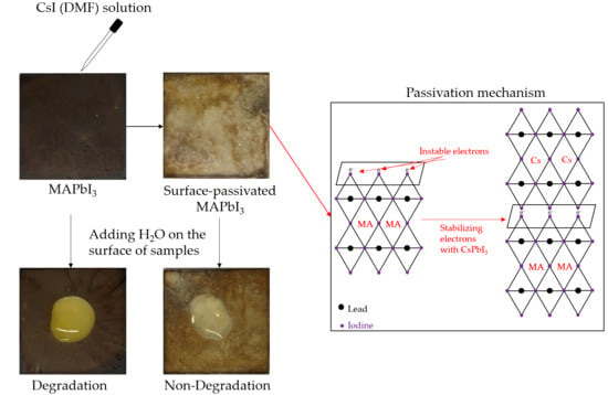
0.692 g PbI2 and 0.159 g MAI were dissolved in 1.5 mL DMF, which gave 1 M PbI2 and 0.75 M MAI solution (A). 1 mL 0.5M CsI was added to 0.5 mL solution A, named solution B. The solutions were pre-heated to 70 °C to ensure all solutes were fully dissolved. The FTO glass was first cleaned with reagent ethanol and reagent acetone and then dried in the oven at 450 °C for one hour. After the cooling process, the FTO glass was transferred to the glovebox. An amount of 0.2 mL of the solution A was dropped on the surface of the FTO glass for spin-coating at a speed of 4000 rpm for 30 s. Then the sample was placed in an oven, annealed at 90 °C for one hour, and thus named Sample A. Solution B (0.2 mL) was uniformly drop-cast on the surface of the FTO glass and then dried in the oven at 90 °C for one hour, and named Sample B. A third sample (the same as A) was made before adding 0.4 mL CsI (0.5 M) solution to the top surface, and then dried in the oven at 90 °C for one hour. The last sample was surface-passivated and named Sample C, which had a slightly whiter surface appearance due to the CsI crystallizations. Synthesis procedures are presented in Figure 1.
2.3. Characterization
Sample A (MAPbI3/FTO, excess PbI2), sample B (PbI2 /MAI/CsI solution/FTO), and sample C (MAPbI3/FTO surface-passivated with CsI solution) as well as a blank FTO-glass, were used for the characterization. Sample A was the base material for sample B and C, which consisted of MAPbI3 and PbI2. Sample B was designed to simulate the interface when surface-passivation CsI was applied on the surface of sample A (MAPbI3), while sample C indicated the surface structure of PSCs after the passivation by CsI. Therefore, the substrate, interface and surface structure could be obtained from the characterization of sample A, B, and C. Blank FTO was used for calibration.
Sample A, B, and C were characterized by micro-photoluminescence with a 60X objective lens and argon ion laser source. The crystal structure of samples was characterized using a Bruker D8 DISCOVERY diffractometer to measure the crystal structure of the materials. The angle 2θ varied from 6° to 88° with a step size of 0.02°. Afterward, sample A, B, and C were surface-characterized using a JOEL 7000 scanning electron microscope (SEM), with a 5 kV electron beam. Sample C was analyzed by energy dispersive x-ray spectroscopy (EDS) in the same SEM. Finally, Samples were simultaneously dropped with 0.05 mL DI-water on the surface center of materials. The time duration starting from water-surface contact to yellow phase appearance was recorded as the degradation time. Yellow phase was the degradation product PbI2, which was a strong indicator of water-induced MAPbI3 degradation.
3. Results and Discussion
3.1. Water Resistance Test
Based on previous experimental results [13], MAPbI3 perovskite layers degrade rapidly when contact with water molecules in the air, producing a strong degradation indicator: yellow lead iodide (PbI2). Thus, a direct water dropping method on the top surface of the samples was applied to speed up the degradation process from months to hours, which provides a simple and time-effective approach to observe the possible degradation of the samples.
As demonstrated in Figure 2a, sample A, which contains MAPbI3 perovskite, degraded immediately, forming a large area of yellow lead iodide after the water-droplet. The degradation process of sample B required ~10 s for the decomposition of the surface. The surface-passivated sample C required over 60 min, to present a very limited trace of degradation, which shows little PbI2 in Figure 2f.
3.2. X-ray Diffraction (XRD)
X-ray diffractometry was conducted to trace the variations of compositional/structural differences between Sample B and Sample C. The time duration before conducting XRD experiments had little influence on the sample crystal structures. Characteristic XRD peaks for MAPbI3, CsPbI3 and CsI were obtained from the database, which are indicated by the Miller Index of different color in Figure 3. The information regarding crystal structures for MAPbI3, CsPbI3, and CsI in our experiments are presented in Table 1. Referring to the results in Figure 3, where the peaks are labelled with the Miller Index in different colors respectively, Samples B and C indicate characteristic XRD peaks for both tetragonal MAPbI3 and rhombohedral CsPbI3 when the 2θ value is small. There was little trace of cubic CsI in Sample B due to the reaction with PbI2, while Sample C had a high intensity of cubic CsI composition. With a higher 2θ value, variations of characteristic peaks were observed.
The XRD experiments were conducted for control group sample B and surface-passivated sample C after the water-treatment on the surfaces. There were two samples of each group for XRD testing, which include one sample without water-treatment and another with water-treatment. The synthesis of the two samples in each group was identical. As shown in Figure 4, sample B demonstrated a significant composition change due to the degradation process (since sample B was not synthesized as simple perovskite which increased the difficulty in identifying each composition individually, it is not indexed in the diagram). Despite the intensity difference caused by slightly different concentrations during spin-coating process, as indicated by Figure 5, sample C had little difference in the crystal composition which is presented by the similar 2 theta peaks of each major content. Thus, the water-stability of surface-passivated perovskite could be verified.
3.3. Scanning Electron Microscopy (SEM)
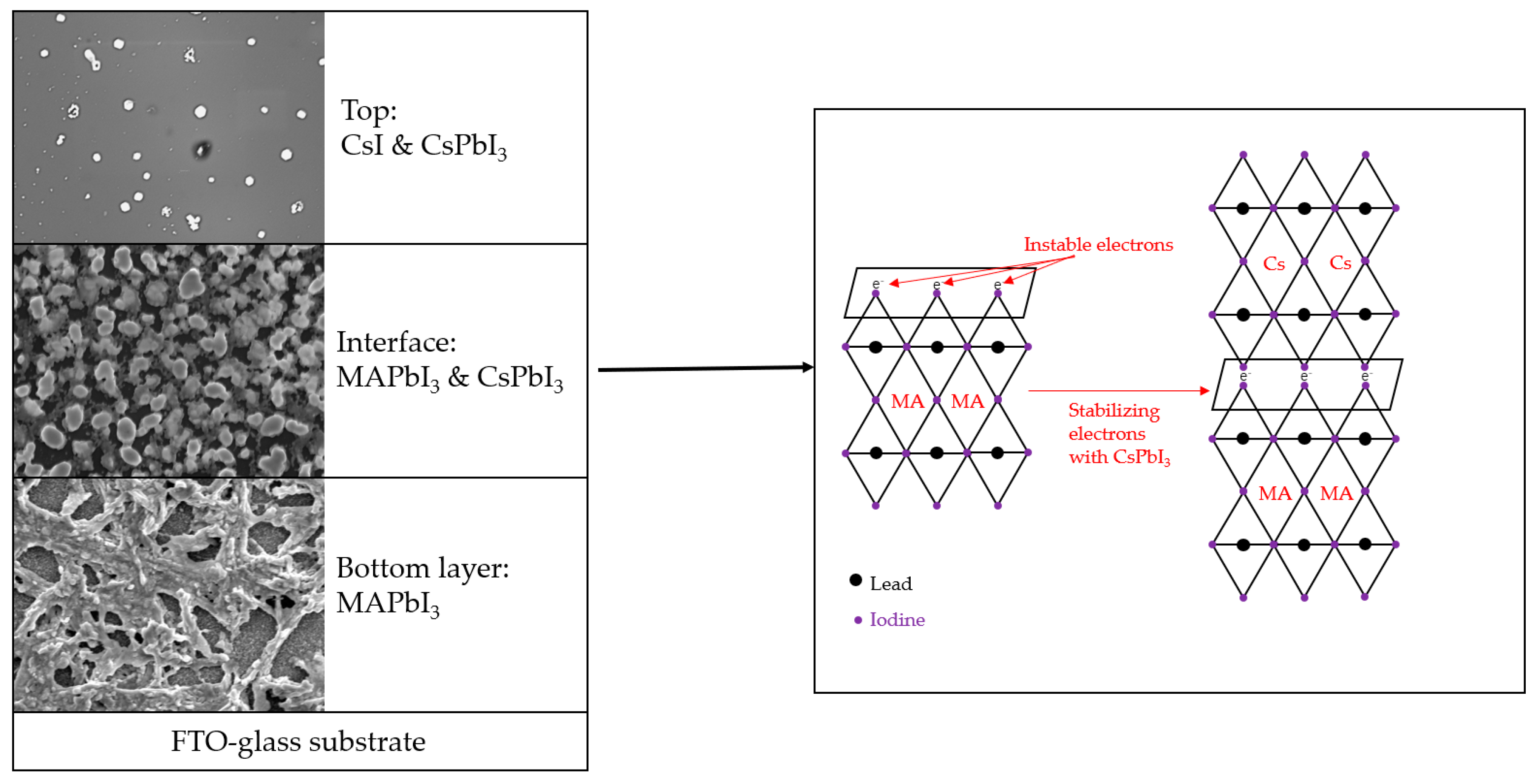
SEM was employed to study the microstructure in detail. According to the literature, the crystal shape of MAPbI3 crystals under SEM is determined by the composition of MAI and PbI2 during the synthesis process, which could be summarized by two types, dendritic appearance when PbI2:MAI ratio is higher than 0.70, and distinguishable crystals when the ratio is lower than 0.70 [19]. In our case, the ratio is 1.33, which means the crystal shape would be dendrite. Sample A fits perfectly with such prediction, as shown in Figure 6A; while sample B in Figure 6B, shows circular-shape dots uniformly dispersed in the dark background, even though it has the same ratio (PbI2: MAI) as the sample A before mixing with CsI. The SEM morphology of sample C (PbI2: (MAI/CsI) ratio = 0.57) shows a similar perovskite crystal shape to that of Sample B. Beneath the CsI layer, the CsPbI3 crystallized around MAPbI3 crystals, as a product of the reaction between excess PbI2 and added CsI. Such observations are further verified by the following energy dispersive X-ray spectroscope (EDS) results.
3.4. Energy Dispersive X-ray Spectroscope (EDS)
From the EDS results in Figure 7, the surface of sample C contains CsI/CsPbI3, as well as base material MAPbI3. Combined with SEM morphology, the layer beneath has a similar structure and composition with sample B: MAPbI3 crystals surrounded by CsPbI3. The bottom layer is made of MAPbI3 crystals.
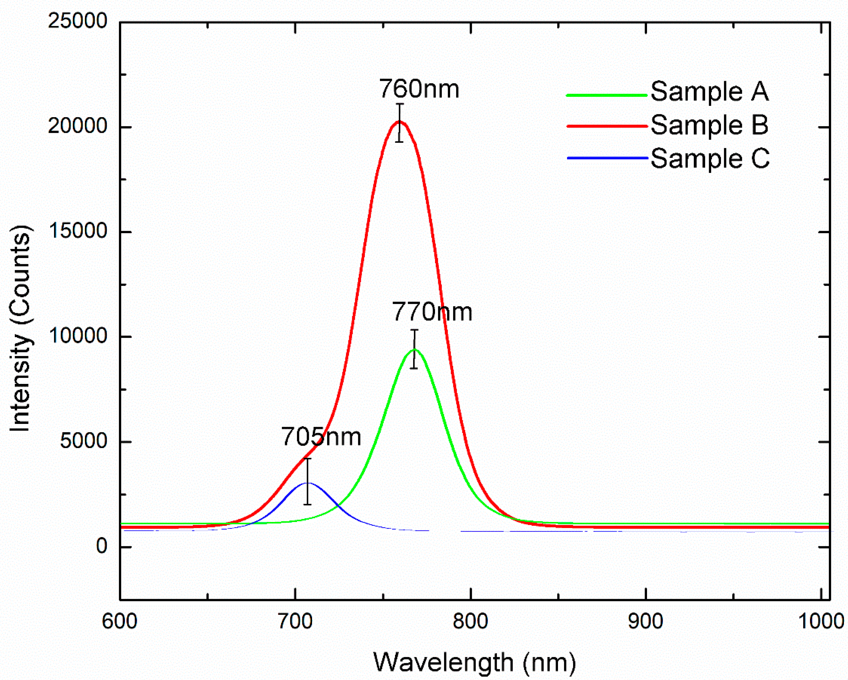
3.5. Photoluminescence (PL)
Photoluminescence was performed to measure the band gap energy, which is given by the location of the spectral absorption peaks in Figure 8.
The results demonstrate that sample A (MAPbI3) has a 1.61 eV band gap that is approximately the same as the literature result [14]. A small blue shift is observed in sample B, resulting in a band gap energy of 1.63 eV. Although the band gap energy of sample C goes up to 1.76 eV which is 150 meV larger than MAPbI3, indicating around 10% less effectiveness to form the electron-hole pairs through PV effect, it is still much smaller than that of inorganic perovskite CsPbI3 [20].
3.6. Discussion
The direct-contact water resistance of hybrid organic perovskite material has been increased from barely 1 s to hours; while the sacrifice in the band gap energy is limited, leading to a successful balance between stability and PL property. The properties of 2 typical perovskite materials and surface-passivated perovskite are presented in Table 2.
Based on previous findings on perovskite materials [16,17,18], the instability of MAPbI3 perovskite is due to the metastable iodine atoms at the interface of crystals, especially near the layer surface. When MAPbI3 perovskite crystals are exposed to moisture, water molecules will bind with metastable iodine and decompose the perovskite structure by penetrating through perovskite crystals. Thus, the key point for solving the instability issue is to stabilize those metastable iodine atoms. Metal halides, such as copper iodide (CuI) or potassium iodide (KI), have been tested to resolve the issue of unstable electrons of iodine [21,22]. Unfortunately, they showed good improvement in other properties like luminescence, but not chemical stability [21,22]. In our experiments, we used chemically-stable inorganic CsI and CsPbI3 to stabilize the active iodine atoms. The excess reactants will precipitate around grain boundaries of perovskite crystals [23], which means the added CsI would react with excess PbI2 in the grain boundaries of MAPbI3 crystals, forming inorganic perovskite precipitates around MAPbI3. The remaining CsI and CsPbI3 would strongly bind with unstable iodine in MAPbI3 crystals. With the elimination of “weak sites”, hybrid organic perovskite would be more resistant to environmental erosions, especially moisture. In addition, CsPbI3 has high chemical resistance to water molecules, therefore, the binding-reinforced layer would be protective for the inner MAPbI3 layer [24].
Structurally, the surface-passivated sample consists of three different layers, as shown in Figure 9. The bottom layer is the main body, which is MAPbI3 crystals, providing a good electron-hole pairs separation efficiency. In the middle layer, CsPbI3 inorganic perovskite is created around the crystals of MAPbI3, stabilizing the halide atoms by eliminating the weak sites. Those inorganic perovskite crystals will protect the inner layer with the help of CsI at the surface layer from the environmental erosions.
4. Conclusions
In our research, we introduced CsI as a surface protection layer on MAPbI3, created a moisture-resistant layer of CsI on the surface, and eliminated the weak sites by establishing bindings between the metastable electrons and CsPbI3. They will block the direct engagement of water molecules with inner perovskite materials and stop moisture-induced degradation. The photoluminescence showed great photovoltaic property, resulting in an excellent balance between stability and performance. While working on the device fabrication and characterizations, we hope to share the new findings with the community, to expedite the progress in ultimately resolving the PSC stability. By exploring the context of properties characterizations and performance examinations, the surface-passivation by inorganic perovskite method could be used as a new technique for hybrid organic perovskite protection.
Author Contributions
Conceptualization, methodology, writing—original, draft preparation, E.G.T.; writing—review and editing, R.T.W. & J.Y.C.; supervision, project administration, G.X.
Funding
This research was funded by the Natural Science and Engineering Research Council of Canada, grant number 105-46964.
Acknowledgments
The authors acknowledge the support from Canadian Center of Electron Microscopy, McMaster Analytical X-Ray diffraction Facility, and McMaster Photovoltaics Laboratory of Engineering Physics.
Conflicts of Interest
There are no conflicts to declare.
References
- Kojima, A.; Teshima, K.; Shirai, Y.; Miyasaka, T. Organometal Halide Perovskites as Visible-Light Sensitizers for Photovoltaic Cells. J. Am. Chem. Soc. 2009, 131, 6050–6051. [Google Scholar] [CrossRef] [PubMed]
- Green, M.A.; Hishikawa, Y.; Dunlop, E.D.; Levi, D.H.; Hohl-Ebinger, J.; Ho-Baillie, A.W.Y. Solar cell efficiency tables (version 51). Prog. Photovolt. Res. Appl. 2018, 26, 3–12. [Google Scholar] [CrossRef]
- Ono, L.K.; Qi, Y. Research progress on organic–inorganic halide perovskite materials and solar cells. J. Phys. D Appl. Phys. 2018, 51, 093001. [Google Scholar] [CrossRef]
- Otte, K.; Makhova, L.; Braun, A.; Konovalov, I. Flexible Cu(In,Ga)Se2 thin-film solar cells for space application. Thin Solid Films 2006, 511–512, 613–622. [Google Scholar] [CrossRef]
- Asghar, M.I.; Zhang, J.; Wang, H.; Lund, P.D. Device stability of perovskite solar cells—A review. Renew. Sustain. Energy Rev. 2017, 77, 131–146. [Google Scholar] [CrossRef]
- Stoumpos, C.C.; Malliakas, C.D.; Kanatzidis, M.G. Semiconducting tin and lead iodide perovskites with organic cations: phase transitions, high mobilities, and near-infrared photoluminescent properties. Inorg. Chem. 2013, 52, 9019–9038. [Google Scholar] [CrossRef]
- Pering, S.R.; Deng, W.; Troughton, J.R.; Kubiak, P.S.; Ghosh, D.; Niemann, R.G.; Brivio, F.; Jeffrey, F.E.; Walker, A.B.; Islam, M.S.; et al. Azetidinium lead iodide for perovskite solar cells. J. Mater. Chem. A 2017, 5, 20658–20665. [Google Scholar] [CrossRef]
- Wang, R.T.; Tai, E.G.; Chen, J.Y.; Xu, G.; LaPierre, R.; Goktas, N.I.; Hu, N. A KMnF3 perovskite structure with improved stability, low bandgap and high transport properties. Ceram. Int. 2019, 45, 64–68. [Google Scholar] [CrossRef]
- Zheng, X.; Wu, C.; Jha, S.K.; Li, Z.; Zhu, K.; Priya, S. Improved Phase Stability of Formamidinium Lead Triiodide Perovskite by Strain Relaxation. ACS Energy Lett. 2016, 1, 1014–1020. [Google Scholar] [CrossRef]
- Han, Q.; Bae, S.H.; Sun, P.; Hsieh, Y.T.; Yang, Y.M.; Rim, Y.S.; Zhao, H.; Chen, Q.; Shi, W.; Li, G.; et al. Single Crystal Formamidinium Lead Iodide (FAPbI3): Insight into the Structural, Optical, and Electrical Properties. Adv. Mater. 2016, 28, 2253–2258. [Google Scholar] [CrossRef]
- Colella, S.; Mosconi, E.; Fedeli, P.; Listorti, A.; Gazza, F.; Orlandi, F.; Ferro, P.; Besagni, T.; Rizzo, A.; Calestani, G.; et al. MAPbI3-xClx Mixed Halide Perovskite for Hybrid Solar Cells: The Role of Chloride as Dopant on the Transport and Structural Properties. Chem. Mater. 2013, 25, 4613–4618. [Google Scholar] [CrossRef]
- Wang, J.T.; Ball, J.M.; Barea, E.M.; Abate, A.; Alexander-Webber, J.A.; Huang, J.; Saliba, M.; Mora-Sero, I.; Bisquert, J.; Snaith, H.J.; et al. Low-temperature processed electron collection layers of graphene/TiO2 nanocomposites in thin film perovskite solar cells. Nano Lett. 2014, 14, 724–730. [Google Scholar] [CrossRef] [PubMed]
- Han, Y.; Meyer, S.; Dkhissi, Y.; Weber, K.; Pringle, J.M.; Bach, U.; Spiccia, L.; Cheng, Y.-B. Degradation observations of encapsulated planar CH3NH3PbI3 perovskite solar cells at high temperatures and humidity. J. Mater. Chem. A 2015, 3, 8139–8147. [Google Scholar] [CrossRef]
- Kim, H.S.; Lee, C.R.; Im, J.H.; Lee, K.B.; Moehl, T.; Marchioro, A.; Moon, S.J.; Humphry-Baker, R.; Yum, J.H.; Moser, J.E.; et al. Lead iodide perovskite sensitized all-solid-state submicron thin film mesoscopic solar cell with efficiency exceeding 9%. Sci. Rep. 2012, 2, 591. [Google Scholar] [CrossRef] [PubMed]
- Mahmood, K.; Swain, B.S.; Amassian, A. 16.1% Efficient Hysteresis-Free Mesostructured Perovskite Solar Cells Based on Synergistically Improved ZnO Nanorod Arrays. Adv. Energy Mater. 2015, 5, 1500568. [Google Scholar] [CrossRef]
- Noel, N.K.; Abate, A.; Stranks, S.D.; Parrott, E.S.; Burlakov, V.M.; Goriely, A.; Henry, J.S. Enhanced Photoluminescence and Solar Cell Performance via Lewis Base Passivation of Organic-Inorganic Lead Halide Perovskites. Am. Chem. Soc. 2014, 8, 9815–9821. [Google Scholar] [CrossRef] [PubMed]
- Shi, J.; Xu, X.; Li, D.; Meng, Q. Interfaces in perovskite solar cells. Small 2015, 11, 2472–2486. [Google Scholar] [CrossRef]
- Mosconi, E.; Ronca, E.; De Angelis, F. First-Principles Investigation of the TiO2/Organohalide Perovskites Interface: The Role of Interfacial Chlorine. J. Phys. Chem. Lett. 2014, 5, 2619–2625. [Google Scholar] [CrossRef]
- Wang, Q.; Shao, Y.; Dong, Q.; Xiao, Z.; Yuan, Y.; Huang, J. Large fill-factor bilayer iodine perovskite solar cells fabricated by a low-temperature solution-process. Energy Environ. Sci. 2014, 7, 2359–2365. [Google Scholar] [CrossRef]
- Sutton, R.J.; Eperon, G.E.; Miranda, L.; Parrott, E.S.; Kamino, B.A.; Patel, J.B.; Hörantner, M.T.; Johnston, M.B.; Haghighirad, A.A.; Moore, D.T.; et al. Bandgap-Tunable Cesium Lead Halide Perovskites with High Thermal Stability for Efficient Solar Cells. Adv. Energy Mater. 2016, 6, 1502458. [Google Scholar] [CrossRef]
- Abdi-Jalebi, M.; Andaji-Garmaroudi, Z.; Cacovich, S.; Stavrakas, C.; Philippe, B.; Richter, J.M.; Alsari, M.; Booker, E.P.; Hutter, E.M.; Pearson, A.J.; et al. Maximizing and stabilizing luminescence from halide perovskites with potassium passivation. Nature 2018, 555, 497–501. [Google Scholar] [CrossRef] [PubMed]
- Sepalage, G.A.; Meyer, S.; Pascoe, A.; Scully, A.D.; Huang, F.; Bach, U.; Cheng, Y.-B.; Spiccia, L. Copper(I) Iodide as Hole-Conductor in Planar Perovskite Solar Cells: Probing the Origin ofJ-VHysteresis. Adv. Funct. Mater. 2015, 25, 5650–5661. [Google Scholar] [CrossRef]
- Son, D.-Y.; Lee, J.-W.; Choi, Y.J.; Jang, I.-H.; Lee, S.; Yoo, P.J.; Shin, H.; Ahn, N.; Choi, M.; Kim, D.; et al. Self-formed grain boundary healing layer for highly efficient CH3 NH3 PbI3 perovskite solar cells. Nat. Energy 2016, 1, 16081. [Google Scholar] [CrossRef]
- Protesescu, L.; Yakunin, S.; Bodnarchuk, M.I.; Krieg, F.; Caputo, R.; Hendon, C.H.; Yang, R.X.; Walsh, A.; Kovalenko, M.V. Nanocrystals of Cesium Lead Halide Perovskites (CsPbX(3), X = Cl, Br, and I): Novel Optoelectronic Materials Showing Bright Emission with Wide Color Gamut. Nano Lett. 2015, 15, 3692–3696. [Google Scholar] [CrossRef] [PubMed]
Figure 1.
Synthesis of sample A (MAPbI3), sample B (a mixture of MAPbI3, CsI, and CsPbI3) and sample C (surface-passivated MAPbI3). MAI: methylammonium iodide; FTO: fluorine-doped tin oxide.
Figure 1.
Synthesis of sample A (MAPbI3), sample B (a mixture of MAPbI3, CsI, and CsPbI3) and sample C (surface-passivated MAPbI3). MAI: methylammonium iodide; FTO: fluorine-doped tin oxide.

Figure 2.
Water-induced degradation experiments ((a–c) are the original images of sample A, B and C before introducing water; (d–f) are the water-contact results of sample A, B, C after 1 s, 10 s, 60 min).
Figure 2.
Water-induced degradation experiments ((a–c) are the original images of sample A, B and C before introducing water; (d–f) are the water-contact results of sample A, B, C after 1 s, 10 s, 60 min).

Figure 3.
X-ray diffraction (XRD) results for sample A, B and C when compared to MAPbI3, CsPbI3, and CsI (before water-treatment).
Figure 3.
X-ray diffraction (XRD) results for sample A, B and C when compared to MAPbI3, CsPbI3, and CsI (before water-treatment).

Figure 4.
XRD results for sample B (before and after water-treatment).

Figure 5.
XRD results for sample C (before and after water-treatment).

Figure 6.
Scanning electron microscopy (SEM) results for sample (A) (MAPbI3), (B) (Mixed MAPbI3, CsPbI3), and (C) (MAPbI3 with CsI &CsPbI3 surface-passivation).
Figure 6.
Scanning electron microscopy (SEM) results for sample (A) (MAPbI3), (B) (Mixed MAPbI3, CsPbI3), and (C) (MAPbI3 with CsI &CsPbI3 surface-passivation).

Figure 7.
Energy dispersive X-ray spectroscope (EDS) analysis for surface-passivated sample.

Figure 8.
Photoluminescence results.

Figure 9.
Layered structure of surface-passivated MAPbI3 perovskite solar cell.


Table 1.
Crystal data of CsPbI3 & MAPbI3.
| Structure | Chemical Formula | Crystal System | Space Group |
|---|---|---|---|
| MAPbI3 | CH3NH3PbI3 | Tetragonal | I4cm |
| CsPbI3 | CsPbI3 | Rhombohedral | R-3c |
| CsI | CsI | Cubic | Pm-3m |
Table 2.
Properties of perovskite materials for solar cell [20].
Table 2.
Properties of perovskite materials for solar cell [20].
| Structure | Band Gap Energy (eV) | Water Resistance | Phase Transition |
|---|---|---|---|
| MAPbI3 | 1.61 | Very poor | NO |
| CsPbI3 | 1.92 | Extremely Good | YES |
| Surface-passivated MAPbI3 | 1.76 | Extremely Good | NO |
© 2019 by the authors. Licensee MDPI, Basel, Switzerland. This article is an open access article distributed under the terms and conditions of the Creative Commons Attribution (CC BY) license (http://creativecommons.org/licenses/by/4.0/).
Share and Cite
MDPI and ACS Style
Tai, E.G.; Wang, R.T.; Chen, J.Y.; Xu, G. A Water-Stable Organic-Inorganic Hybrid Perovskite for Solar Cells by Inorganic Passivation. Crystals 2019, 9, 83. https://doi.org/10.3390/cryst9020083
AMA Style
Tai EG, Wang RT, Chen JY, Xu G. A Water-Stable Organic-Inorganic Hybrid Perovskite for Solar Cells by Inorganic Passivation. Crystals. 2019; 9(2):83. https://doi.org/10.3390/cryst9020083
Chicago/Turabian StyleTai, Edward Guangqing, Ryan Taoran Wang, Jason Yuanzhe Chen, and Gu Xu. 2019. "A Water-Stable Organic-Inorganic Hybrid Perovskite for Solar Cells by Inorganic Passivation" Crystals 9, no. 2: 83. https://doi.org/10.3390/cryst9020083
Note that from the first issue of 2016, this journal uses article numbers instead of page numbers. See further details here.