1. Introduction
In recent years, 2D materials including inorganic layered crystals and organic thin films have gained considerable interest owing to their wide applications. Besides crystal materials existing in nature, we have witnessed how scientists create 2D materials via materials synthesis and fabrication strategies. In particular, among these materials, the preparation and characterization of amorphous carbon (a-carbon)-based films have drawn a special consideration due to their possible applications in magnetic sensing, gas sensing, solar cells, and optoelectronics, to name just a few [
1,
2,
3,
4,
5].
The a-carbon is one of the allotropes of carbon for which the magnetotransport properties significantly depend on the structural disorder in thin films. In a-carbon, the degree of disorder influences the conductivity of the materials [
6,
7,
8,
9]. Much work has been done on the exploration of the magnetotransport properties and the mechanisms of such transport properties of pure a-carbon materials. Despite much effort devoted to the field, there are many sides to the transport properties of such a-carbon and they are still worth investigating [
10,
11,
12]. Owing to magnetic field applications, for higher magnetic fields the MR of a-carbon persists unsaturated, and the relationship between magnetotransport and spintronics made the undoped a-carbon a more attractive candidate. A number of studies on the magnetotransport properties of doped a-carbon have been reported, but the area of pure a-carbon is still a popular and active field of research [
13,
14,
15,
16,
17].
Pure a-carbon has attracted a significant importance as a result of its involvement in the direct impact of the amorphous nature of carbon on the magneto transport properties of a-carbon, and mostly undoped a-carbon has MR properties only in low temperature regions, which are mainly important for mechanism studies [
18,
19,
20,
21]. On the other hand, MR studies at higher temperatures up to room temperature, is very much important for different applications. Our group studied several types of MR properties, such as Positive MR, Negative MR and Angular MR of a-carbon films deposited via different fabrication techniques like the CVD technique and PLD technique [
22,
23,
24,
25]. Jimin et al. reported a larger magnitude of positive MR of 36% measured at the field of 12 T for pure a-carbon thin film samples deposited via the PLD method, and the wave function shrinkage theory was ascribed as the suitable mechanism for such MR. The MR was only observed in low temperature regimes from 2 K to 80 K [
26]. Later, they studied the Fe-doped a-carbon thin films through the same deposition technique and observed an interesting phenomenon, where the MR switched signs from negative MR to positive MR. It has been observed that spin dependent scattering was a mechanism responsible for such sample a-carbon films [
27]. These different MR phenomena have their own significance in a variety of research fields and applications. Consequently, the larger magnitude of angular dependent MR and presence of angular MR up to room temperature is also significantly important for researchers as well as for magnetic sensor applications.
In this paper, thin films of a-carbon have been deposited via the CVD technique. Previously, Sagar et al. [
18,
22] used the CVD technique to grow the amorphous carbon thin films, and after fabrication they always needed to transfer the thin films through chemical etching for further characterizations, which may cause many structural changes and distortions in the specimen thin films. On the other hand, during our fabrication of a-carbon sample thin films, by optimizing different parameters and introducing a sub-cooling step during the growth, we were able to control the film growth in such way that the prepared samples did not need to be transferred through chemical etching for RAMAN, XRD and PPMS characterizations. This transfer-free growth plays an important role in transforming the structural properties and may be ascribed as an influence on the larger value of angular MR. A substantial progress in the angular MR magnitude was attained, and this angular MR can be achieved even up to 300 K.
2. Experiment Method
Using the CVD technique, a-carbon thin films were grown on Si wafers having a 300 nm thick layered SiO2 substrate. To eliminate any surface contamination, the sonication was performed for half an hour on the substrates, before we loaded the substrate to the central position of the tube furnace. The tube furnace was pumped to vacuum until ~10−1 torr. First, by using the ramp rate of 5 K/min, we raised the temperature of the furnace up to 473 K. During the entire experiment, Hydrogen (H2) and Argon (Ar) were used as carrier gases and flowed at flow rates of 40 sccm and 160 sccm, respectively.
Second, the temperature was increased to 1373 K with an increasing rate of 10 K/min, and the annealing of the substrate was conducted at this temperature over 15 min. To grow a-carbon sample films, ethylene (C2H4) was used as the precursor gas and was brought together as a carbon source having a stream rate of 40 sccm. This thin film sample duration for the thin film growth was 10 minutes. The sample films deposited for 10 minutes were named sample S10.
Third, before the cool-down of the tube furnace, we introduced a sub-cooling step for which we held the tube furnace temperature at 1273 K for half an hour. Subsequently, the temperature of the tube furnace was lowered to room temperature. Hydrogen and argon were continuing to flow during the cooling step as well. We deposited the a-carbon films in a way that did not involve any transfer, and all characterizations were performed directly on the sample films, except HRTEM. For HRTEM, we used the chemical etching method to fish out the thin film onto the TEM Cu grid.
A Renishaw InVia Raman microscope (Renishaw, Gloucestershire, United Kingdom) was used to estimate the Raman spectrum with an excitation wavelength of 514 nm. The structure morphology of the sample thin film was studied via JOEL-2011 High Resolution Transmission Electron Microscopy (Jeol, Tokyo, Japan). The Rigaku 2500 X-ray Diffractometer (Rigaku, Austin, TX, USA) was used to analyze the amorphous structure of the sample thin films. Furthermore, the magnetoresistance measurement was done through the quantum design physical property measurement system. The standard indium pressing technique was used to prepare the metal electrodes as shown in
Figure 1b by using the standard four-probe method for a resistance measurement.
3. Results and Discussion
The different growth conditions are responsible to control the structural properties of these thin film sample. The angular magnetoresistance properties are mainly controlled by the structural feature. The structural properties were analyzed by Raman spectroscopy, allegedly the finest nondestructive tool for such a measurement. Other analytical tools were used to estimate the structure properties of the fabricated sample thin film. The amorphous behavior of the sample thin film was estimated through a HRTEM diffraction pattern and image as shown in
Figure 2. The randomly oriented graphitic clusters were also observed at a size of ~5nm on the a-carbon surface. The quantitative estimations for the D-band and G-band content was done through Raman techniques.
Figure 2 shows the HRTEM to investigate the structure of the a-carbon film. The amorphous nature of the sample thin film can be seen by the diffraction pattern and the image as well. Furthermore, the randomly oriented graphite nano-crystals can be assumed from the diffused rings pattern. These patterns indicate that this a-carbon thin film is the mixture of randomly oriented nanocrystals and amorphous carbon.
The average thickness of the sample thin film was measured at around ~44 nm by atomic force microscopy, as shown in
Figure 3b. The π and π* band was raised up due to the nanometer-sized graphitic rings which have a tendency to exist as
sp2 hybridized carbon atoms, whereas the aliphatic chains are due to the existence of the
sp3 hybridized carbons. The D-band corresponds to the breathing mode of A
1g symmetry in the six atoms ring, which is due to the defects, which are needed for its activation; consequently, this band is foremost in the presence of the defects and was not present in the case of graphene [
10,
28]. The in-plan distending gesture of the carbon atom pairs present in both the ring and chain shapes gives rise to the Raman G-band. Moreover, the XRD pattern shown in
Figure 3a also shows evidence of the completely amorphous nature of the prepared sample a-carbon thin film.
The Raman spectrum of the disordered sample a-carbon thin films is shown in
Figure 4, which presents the two major Raman bands as G-band and D-band, positioned at~1574 cm
−1 and ~1330 cm
−1, respectively. The
ID/IG is known as the D-band and G-band intensity ratio, which presents evidence of C(
sp2) content in the thin film specimen. The magnitude of the
ID/IG intensity ratio was found to be 2.11 in this sample.
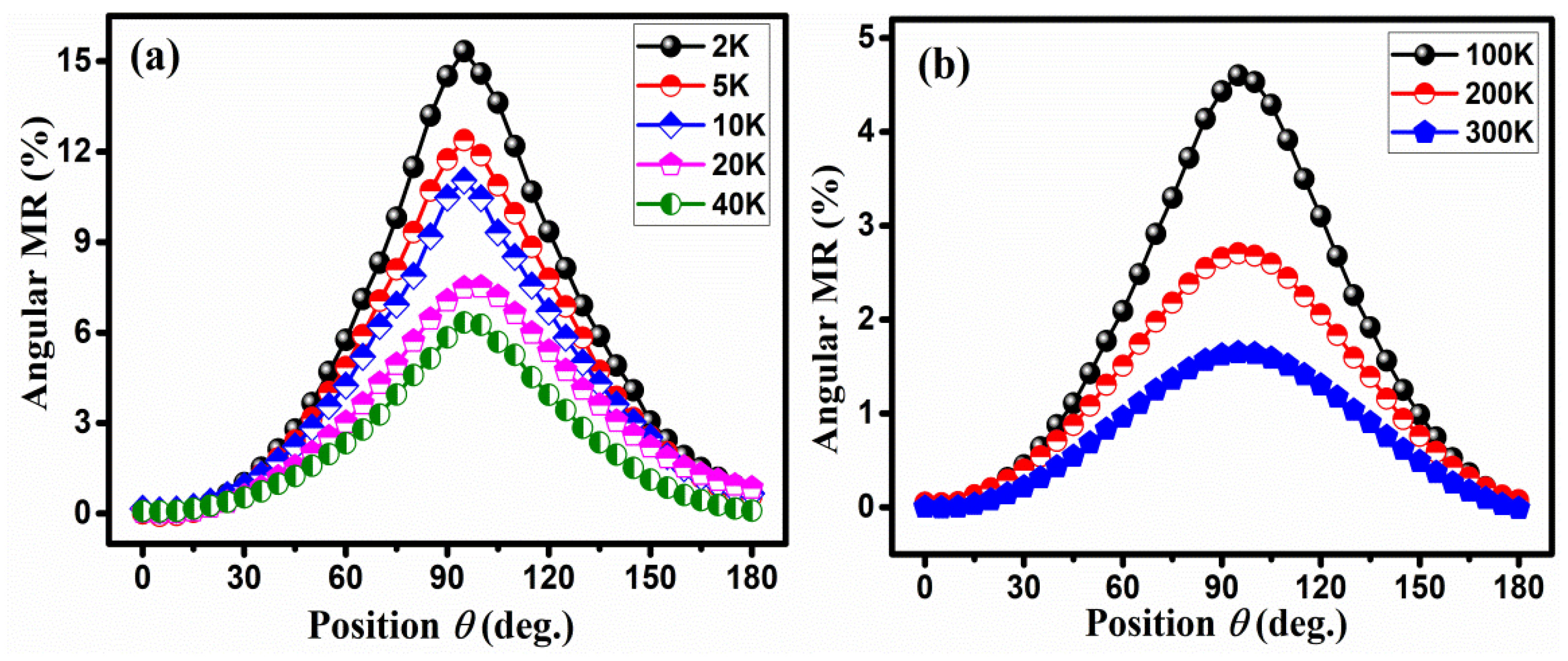
Up to the fixed magnetic field of 7 T, the angular MR of the sample a-carbon film was calculated within a temperature ranging from the lower temperature of 2 K to the room temperature of 300 K. The angular magnetoresistance was calculated by using the variable angle definition [
18].
where
and
represent the measure of the sample resistance at angles of
θ and 0°, respectively. Meanwhile,
θ represents an angle of applied field (
B) to normal of the deposited sample surface (n).
Figure 5 presents the angular MR of pure a-carbon sample thin films, which were studied for the angles ranging from 0°~180° and the temperatures ranging between 2~300 K. The magnitude of the angular MR of ~15% was obtained at 2 K, and the magnitude of ~1.4% was obtained at 300 K, at the fixed field of 7 T and at the angle of 90°, as shown in
Figure 5.
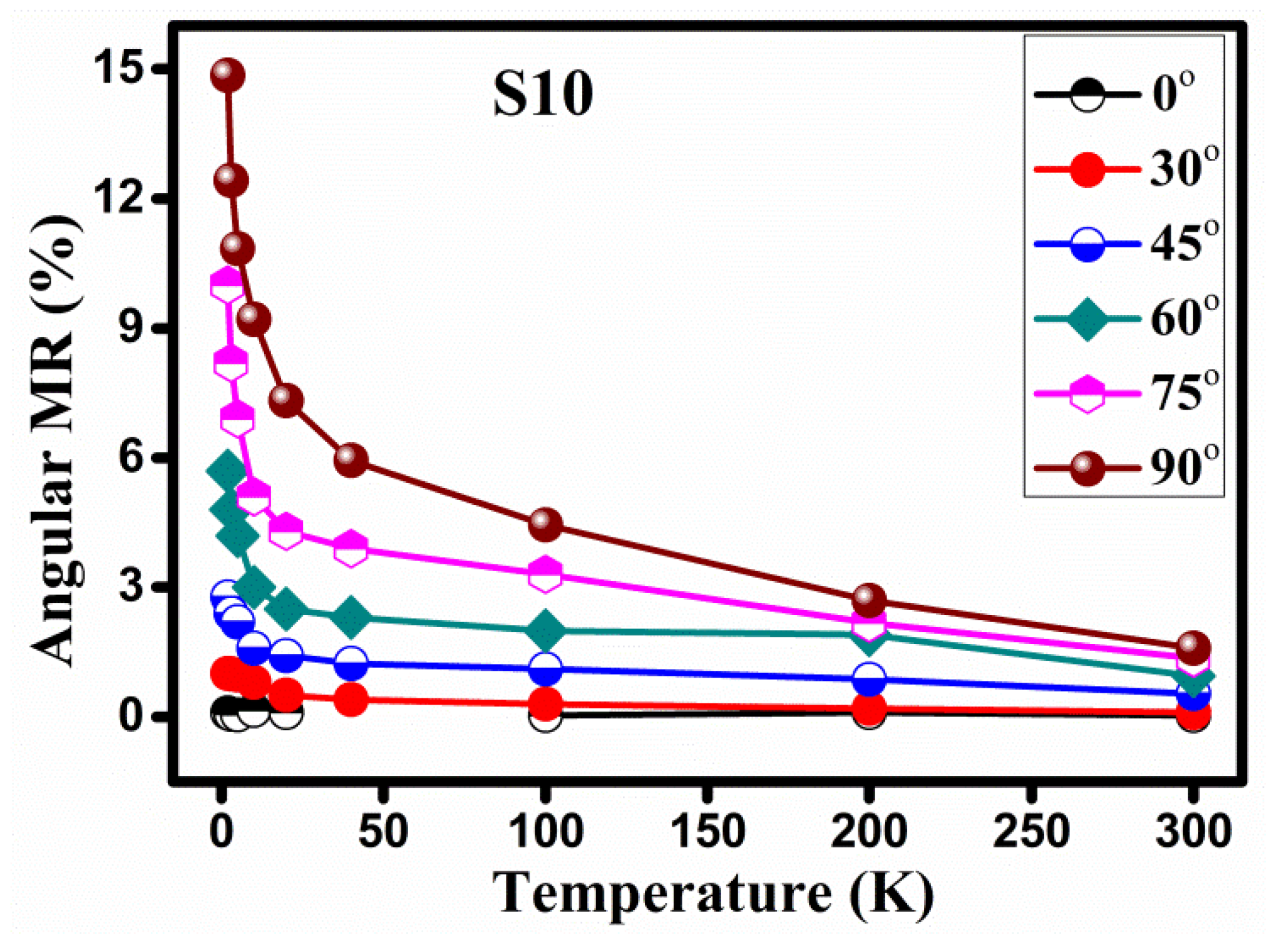
Rotating the sample between 0° to 90°, the angular MR magnitude increases, and the highest magnitude was noticed at an angle of 90°, whereas the value of the angular MR decreased from 90°~180°. An inverse relation was observed between the angular MR magnitude for the sample thin film and the measurement temperature, as presented in
Figure 5. The plot of the angular MR vs. measurement temperature at different angles presented an exponential decay trend, as seen in
Figure 6.
The grain boundary scattering (GBS) conductivity equation might give a suitable explanation for the MR transport mechanism [
23]:
where
A, b, and
C represent constants,
ρ represents resistivity and
P represents the material reliant constant. The average possibility of carriers’ transient via a single boundary is known as
A, where
D =
lo/
RG, while
RG represents the crystallite size of the clusters and
lo is the mean free path. In our carbon samples, the measured average value of
lo is from 3~5 nm.
The scattering from the grain boundaries happens when the electrons flow from the nanocrystalline grains which are entrenched in an amorphous system, and these grain boundaries behave as potential (δ) barriers [
29]. A similar phenomenon is happening for our a-carbon thin films, where 3–5 nm sized graphitic nanocrystallites are embedded in the amorphous carbon matrix. The nanometer sized graphitic clusters can be seen in
Figure 2. Consequently, this a-carbon sample thin film is the combination of both the amorphous and randomly orientated nanometer sized graphitic clusters on the surface. These graphitic clusters may contribute to the transport conduction phenomenon happening in these a-carbon samples thin films.
As compared to the bulk materials, for nanometer dimensions, the grain boundaries and the surface are two major factors on which the electrical resistivity is dependent in nanometer dimensions, as proposed by Mayadas and Shatzkes [
30]. The grains boundaries are normal to the film plane presented by the N parallel planes, where the electric field direction is orientated perpendicular to these planes. Every single grain boundary provides a sturdy δ-function potential which acts as a barrier to transient electrons through the surface. When a certain field is applied, the electrons are scattered from these potential barriers, and as a result some of the electrons will conduct through these boundaries or so-called potential barriers. This is a very useful phenomenon for estimating the resistivity variation trend for the sample thin films which are embedded with the nanocrystalline clusters on the amorphous matrix [
29].
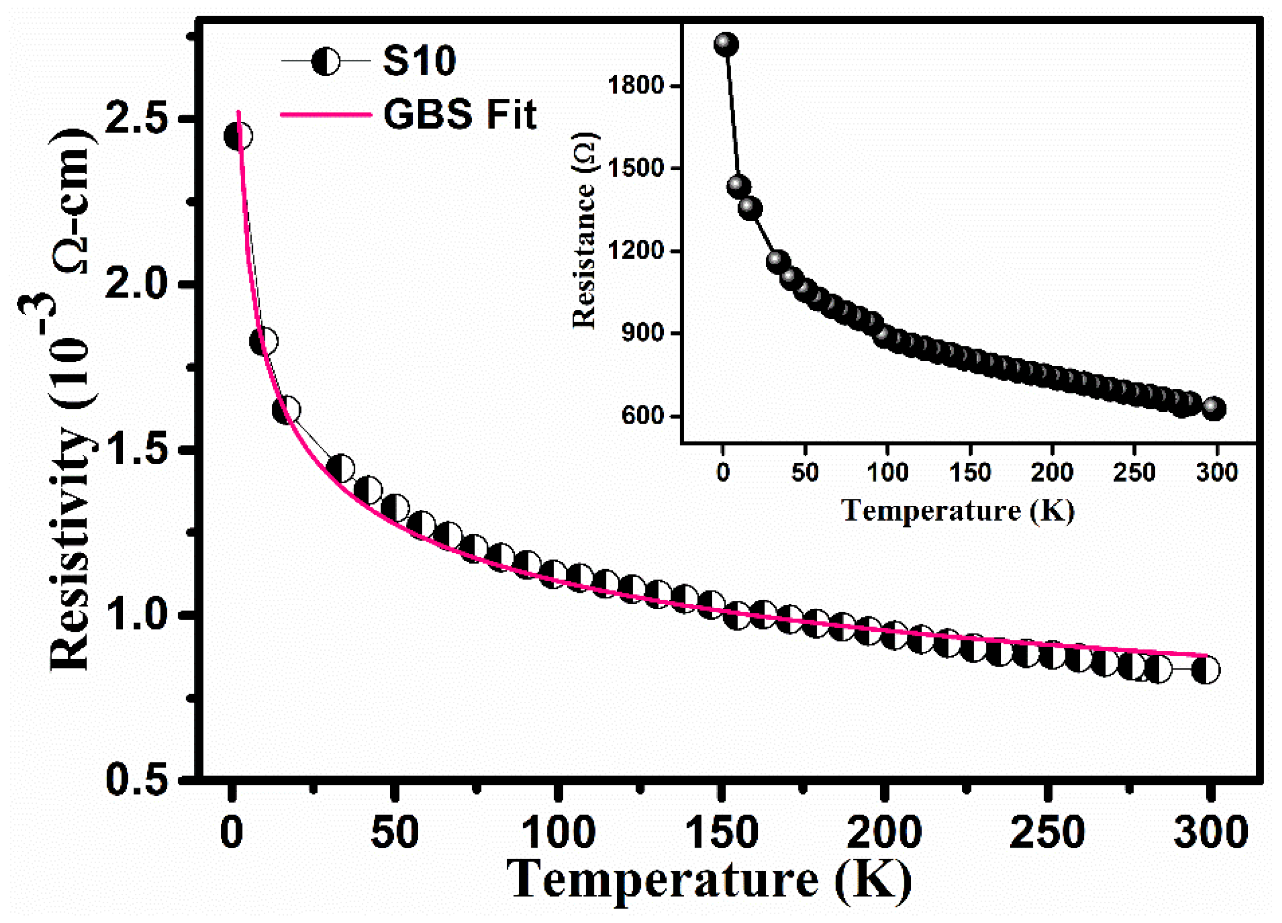
Figure 7 shows that for entire temperature range, the GBS conductivity relation fitted with the resistivity relation. One can also observe that the fit curve is slightly poor with the resistivity plot for lower temperatures such as 20~70 K, and a similar effect can be observed for higher temperatures such as 230~300 K. As such, amorphous carbon systems are still lacking in mechanism studies. Grain boundary scattering is the proposed mechanism study, which might be a suitable mechanism but not be the absolute one. The electron tunneling between the sp
2 clusters may also contribute to the conductivity and to the MR of the films, and this will be studied in the future to investigate further mechanisms of such amorphous carbon systems. The GBS theory also indicates that the Lorentz force caused the bending of the trajectories of charge carriers, when the applied magnetic field and plan are perpendicular to each other. Consequently, the possibility of GBS scattering decreases and the sample resistance shifts to a decrease, as shown in the RT plot (inset
Figure 7, resulting in a decrease of the angular MR for the investigated sample a-carbon thin film. Grain boundaries in the sample thin film rise promptly as a result of the increasing number of graphitic clusters. More defects might be created due to the increment in grain boundaries, which is also what the observed RAMAN data presents. The nano-crystal edges will act as defect boundaries. For the GBS scattering, due to graphitic crystals, the crystals in an a-carbon matrix are greatly dependent on the
sp2 carbon [
18]. Thus, the angular MR in sample a-carbon thin films are attributed to the
sp2 atoms. The GBS effect, together with the increase of disorder, causes an enhancement of the angular MR magnitude. The electron scattering on the boundaries of the grains might not endure the exclusive transport mechanism. The tunneling of the concerned electrons to the
sp2 clusters might offer a contribution to the MR of such sample a-carbon films and to the conductivity of the system.

 ,
, 


