Radiation Tolerance in Nano-Structured Crystalline Fe(Cr)/Amorphous SiOC Composite


1
Department of Mechanical and Materials Engineering, University of Nebraska-Lincoln, Lincoln, NE 68583-0857, USA
2
Department of Nuclear Engineering, Texas A&M University, College Station, TX 77843-3128, USA
3
Nebraska Center for Energy Sciences Research, University of Nebraska-Lincoln, Lincoln, NE 68583-0857, USA
4
Nebraska Center for Materials and Nanoscience, University of Nebraska-Lincoln, Lincoln, NE 68588-0298, USA
*
Author to whom correspondence should be addressed.
Crystals 2019, 9(3), 147; https://doi.org/10.3390/cryst9030147
Submission received: 7 February 2019
/
Revised: 5 March 2019
/
Accepted: 9 March 2019
/
Published: 13 March 2019
(This article belongs to the Special Issue Nanostructured Ferritic Alloys)
Abstract
:The management of irradiation defects is one of key challenges for structural materials in current and future reactor systems. To develop radiation tolerant alloys for service in extreme irradiation environments, the Fe self-ion radiation response of nanocomposites composed of amorphous silicon oxycarbide (SiOC) and crystalline Fe(Cr) were examined at 10, 20, and 50 displacements per atom damage levels. Grain growth in width direction was observed to increase with increasing irradiation dose in both Fe(Cr) films and Fe(Cr) layers in the nanocomposite after irradiation at room temperature. However, compared to the Fe(Cr) film, the Fe(Cr) layers in the nanocomposite exhibited ~50% less grain growth at the same damage levels, suggesting that interfaces in the nanocomposite were defect sinks. Moreover, the addition of Cr to α-Fe was shown to suppress its grain growth under irradiation for both the composite and non-composite case, consistent with earlier molecular dynamic (MD) modeling studies.
1. Introduction
The successful deployment of future nuclear reactors requires structural materials to withstand extreme environments of irradiation and temperature [1,2]. Radiation induced swelling leads to dimensional distortion and embrittlement, and is a life-limiting materials issue for structural materials in nuclear power reactors. Therefore, the management of radiation defects is vital to improving the stability of irradiated alloys [3,4]. This challenge calls for development of revolutionary alloys that are able to resist radiation damage. Over past decades, extensive research has been conducted to introduce defect sinks such as grain boundaries and interfaces to suppress radiation damage accumulation. For example, oxide-dispersion-strengthened (ODS) alloys with interfaces between nanoscale oxides and ferritic/martensitic steels have exhibited superior void swelling resistance because of the sink proficiency of the interface [4,5]. In addition, grain boundaries in austenitic stainless steels have been found to accelerate defect recombination and effectively suppress the void swelling [6,7,8]. In addition, incoherent interfaces in several immiscible metallic nanolayer systems (e.g., interfaces between face-centered cubic and body-centered cubic materials, such as Cu/Nb) were demonstrated to trap and recombine Frenkel pairs created during irradiation-induced collision cascades, and thus mitigate the onset of He bubble formation [9].
Compared to traditional approaches which strive to delay the deleterious effects of radiation damage, amorphous ceramics could be a strong option for high radiation tolerance because they do not contain or evolve conventional crystal defects such as vacancies, interstitials, or dislocations under irradiation. The amorphous silicon oxycarbide (SiOC) crystallization temperature is in excess of 1300 °C and good oxidation and creep resistance has been observed [10,11,12,13]. This model class of amorphous ceramics has exhibited great stability under irradiation, sustaining its glassy state over a wide range of irradiation conditions [14,15]. In addition, it has demonstrated the immunity of He bubble formation by continually removing He as it was implanted [16,17]. For instance, implanted He atoms were found to outgas from the SiOC matrix through atomic-scale diffusion without damaging its free surfaces, even at liquid nitrogen temperatures, resulting in time-invariant structure and properties. To step toward applications, amorphous SiOC can be paired with a crystalline metal component such as Fe to form a composite with enhanced thermal, mechanical, and irradiation properties [18,19,20,21].
Although the crystalline/amorphous interfaces in Fe/SiOC composites have been demonstrated as effective point defect sinks and thus enhance the radiation tolerance of the composite, the irradiation response of Fe(Cr)/SiOC remains uncharted. Using Fe(Cr) as a composite constituent serves as a first step towards realizing and understanding the role of steel in the SiOC based composite in an irradiation environment. Previous work has shown the concentration of chromium (Cr) plays a vital role on the radiation induced microstructure, corrosion, and swelling resistance of the binary Fe(Cr) alloys [22,23,24,25]. The main purpose of the present work is two-fold: (1) investigate irradiation stability of the Fe(Cr)/SiOC composite and the capacity of these interfaces in absorbing radiation induced defects spanning the damage range from 10 to 50 displacement per atom (dpa); (2) examine the effect of Cr on the irradiation response of the nanolayered Fe(Cr)/SiOC composite relative to stand-alone Fe(Cr) films as well as to that of pure Fe films and Fe/SiOC nanolayered composites.
2. Materials and Methods
In this work, both nanocrystalline α-Fe(Cr) and Fe(Cr)/SiOC nanolayers were fabricated by magnetron sputtering. Nanocrystalline Fe(Cr) films were obtained by using direct current (DC) magnetron sputtering from an alloy Fe-Cr target, while amorphous SiOC layers were synthesized by radio frequency (RF) co-sputtering from SiC and SiO2 targets at room temperature. The thickness of α-Fe(Cr) film was approximately 1.7 μm and the energy-dispersive X-ray spectroscope (EDS) analysis suggests the atomic composition of the Fe(Cr) layers was Fe88Cr12. Rutherford backscattering spectrometry suggested that the SiOC films possessed a chemical composition of Si-30%, O-40%, C-30% and X-ray reflectivity results indicate a density of 2.2 g/cm3 [26]. For the Fe(Cr)/SiOC nanolayers, the individual Fe(Cr) and SiOC layer thicknesses were 140 and 80 nm, respectively. Eight alternating Fe(Cr) and SiOC layers were deposited, yielding a total film thickness of approximately 1.8 μm. The base pressure prior to depositions was 1.2 × 10⁻⁵ Pa or lower. The typical Ar partial pressure during sputtering was 0.65 Pa for both Fe(Cr) and SiOC deposition. All specimens were subjected 3.5 MeV Fe ion irradiation at room temperature (RT). A defocused Fe ion beam, 6 mm × 6 mm in size, was used during all irradiations. The fluence was measured by monitoring the charge collection on the target and the fluence variation within the beam spot was typically within ±10%. Maximum temperature of the sample during irradiation was never above 60 °C.
The total fluences of 1.54 × 10¹⁶, 3.08 × 10¹⁶ and 7.70 × 10¹⁶ ions/cm2 were used to create 10, 20, and 50 dpa, respectively, at the depth of 550 nm in the Fe(Cr) films. To obtain the same nominal irradiation damage levels in the Fe(Cr)/SiOC nanolayered composite, fluences of 1.77 × 10¹⁶, 3.54 × 10¹⁶ and 8.85 × 10¹⁶ ions/cm2 were applied. Depth-dependent damage and Fe concentration profiles were calculated with the Stopping and Range of Ions in Matter (SRIM)-2008 simulation package using the ion distribution and quick calculation of damage option (Kinchin-Pease model) [27]. The displacement energies of Si, O and C elements was taken as the default values in the SRIM software as 15 eV for Si, 28 eV for O and C. The displacement energy 40 eV was chosen for both Fe and Cr. The cross-sectional microstructures of all materials, before and after Fe-ion irradiation, were characterized by transmission electron microscopy (TEM, A FEI Tecnai G2 F20). All cross-sectional TEM specimens were prepared by conventional dimple and grinding, followed by ion-milling. To reduce the ion milling damage, a low energy (3.5 keV) and a low angle (5°) were selected.
3. Results
3.1. Microstructural Characterization of As-Deposited Films
Figure 1a,b present typical cross-sectional TEM micrographs of as-deposited Fe(Cr) and Fe(Cr)/SiOC nanolayered composites, respectively. The as-prepared Fe(Cr) layers exhibits a columnar structure, suggesting a Volmer–Weber (VW) growth [28]. An alternating layered structure with sharp interfaces can be observed in the composite films, and all SiOC layers show uniform contrast. The corresponding selective area diffraction (SAD) pattern from the Fe(Cr) exhibits ring diffraction patterns with similar interval spacing, shown in the inset of Figure 1a, indicating a body-centered cubic (BCC) structure. Besides the BCC ring diffraction pattern, the SAD of Fe(Cr)/SiOC composite exhibits a diffusion halo around the central beam, indicating the amorphous nature of the SiOC layer. An alternating Fe(Cr) and SiOC nanolayer structure with clear interfaces can be better observed in Figure 1c,d. The average grain size of the Fe(Cr) in the width direction was determined to be the same for the stand-alone film and the composite, 21 ± 3 nm, while the average grain size of Fe(Cr) in the length direction depends on the thickness of Fe(Cr) layers.
3.2. SRIM Simulation
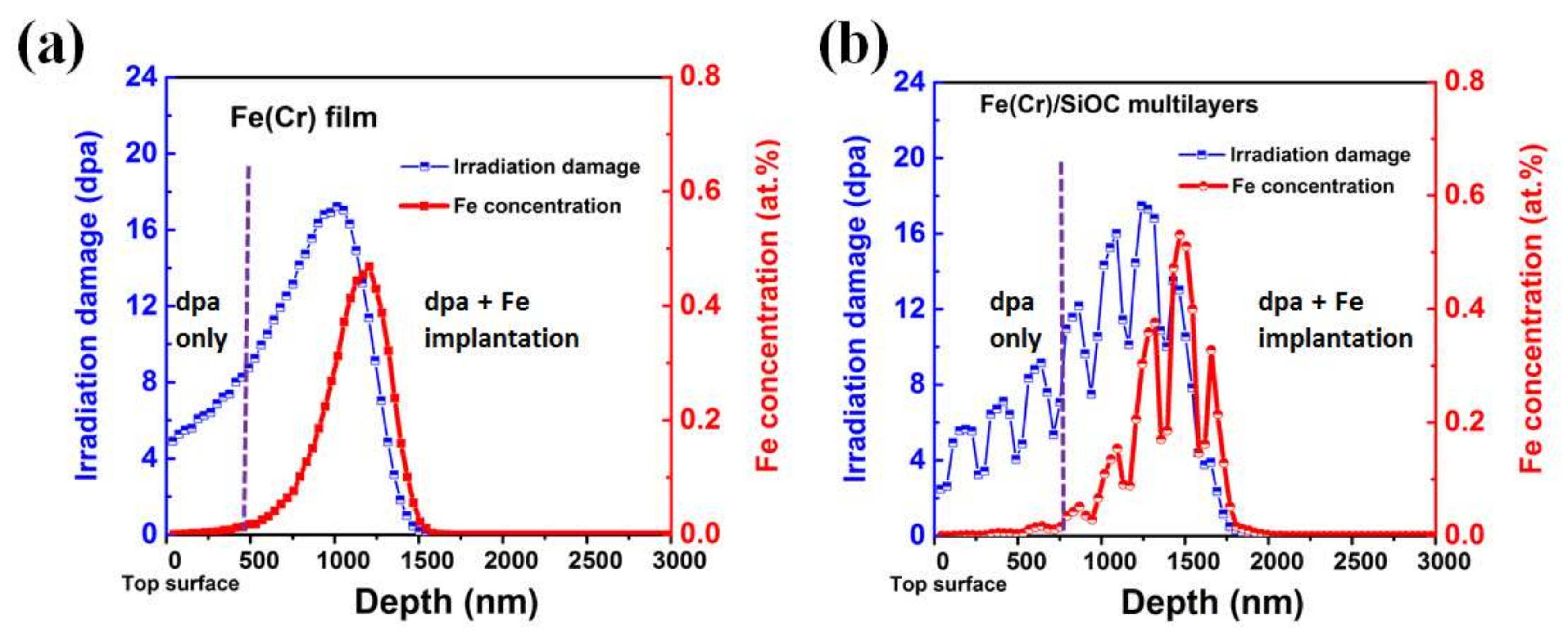
To minimize impurity effects, 3.5 MeV Fe ions were selected for the irradiation. Three different nominal damage levels, 10, 20, and 50 dpa, were applied. Figure 2a,b show the simulated damage (nominal 10 dpa irradiation) and implanted Fe depth profiles in the Fe(Cr), with a dose of 1.54 × 10¹⁶ ions/cm2, and the Fe(Cr)/SiOC nanolayers, with a fluence of 1.77 × 10¹⁶ ions/cm2, respectively. From Figure 2a,b, the Fe irradiations result in approximately 10 dpa of pure irradiation damage (minimal implanted Fe) in the Fe(Cr) films at the depth of 550 nm and in the third Fe(Cr) layer of the Fe/SiOC nanolayered films, respectively. From the simulation of Fe/SiOC nanolayers, the dpa value in Fe(Cr) layers is approximately 2–3 times higher than that of the SiOC layer next to it. As also shown in Figure 2, the majority of Fe ions came to rest at the depth beyond 1 μm and there was a negligible amount of Fe implanted in the near surface region (<800 nm). To avoid possible surface effects on defect migration, the top region from 300 nm below the surface to 800 nm was chosen for the examination of atomic displacement effects on structural evolution.
3.3. Irradiation Response of Fe(Cr) Film and Fe(Cr)/SiOC Multilayer
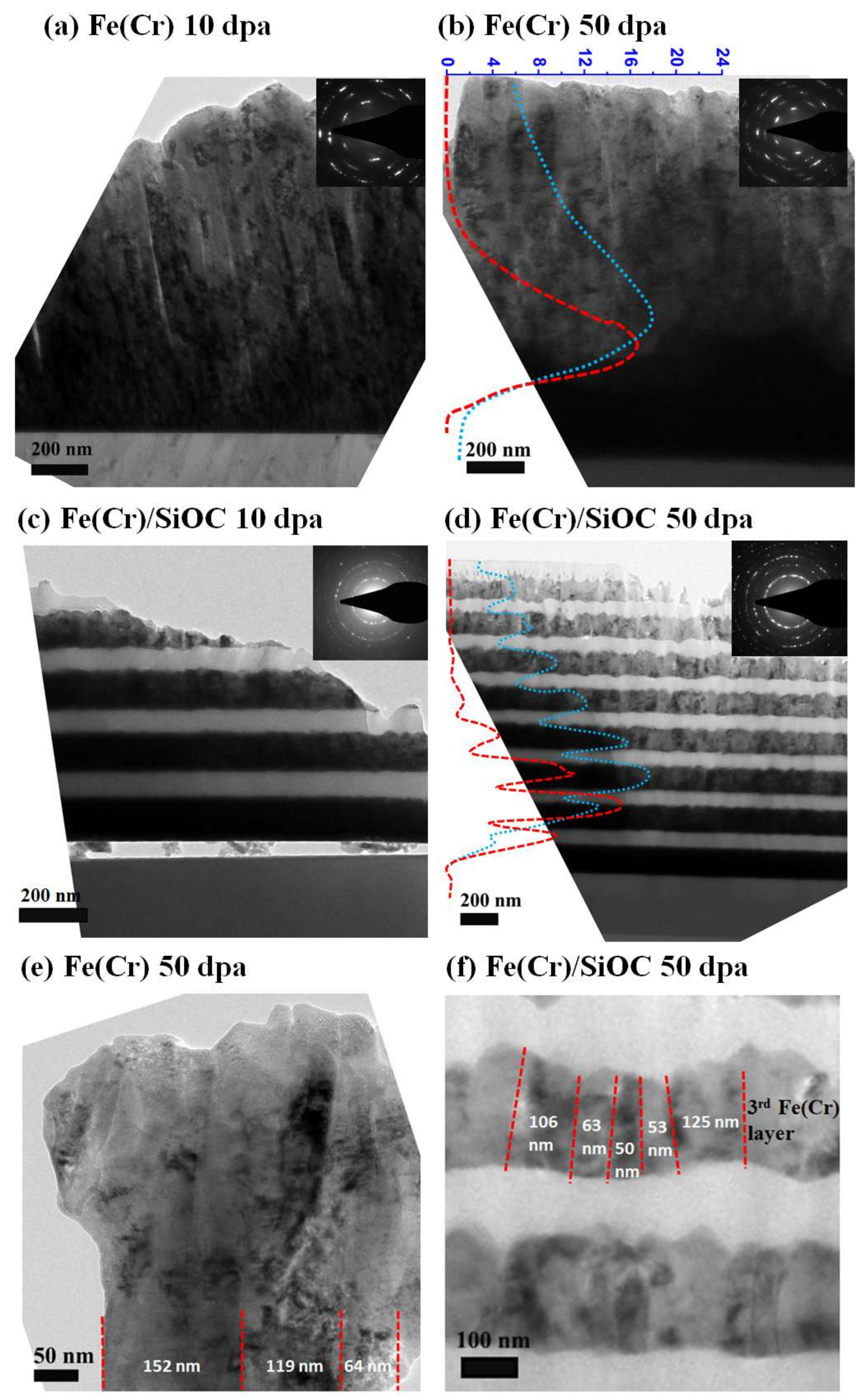
Figure 3a,b show cross-sectional TEM micrographs of the Fe(Cr) films after Fe irradiation to nominal damage levels of 10 and 50 dpa, respectively. The Fe(Cr) films retain their columnar feature and a BCC crystal structure, as evidenced by TEM images and corresponding SAD patterns (seen as inset of Figure 3a,b). However, a monotonic increase in Fe(Cr) grain size in the width direction was observed as a function of damage level. The microstructural evolution of the Fe(Cr)/SiOC specimens after 10 and 50 dpa are presented as Figure 3c,d, respectively. After irradiation, the Fe(Cr)/SiOC composites still maintained their layered structure with sharp interfaces. Very similar SAD patterns were observed after irradiation compared to the as-deposited Fe(Cr)/SiOC composite, suggesting no secondary phase formation or recrystallization occurred. The main observation was irradiation-induced Fe(Cr) grain growth in the Fe(Cr)/SiOC composite. Two typical examples of Fe(Cr) grain growth in the width direction of the Fe(Cr)/SiOC composite after 50 dpa irradiation are shown in Figure 3e,f, respectively. Consistent with SRIM simulations, Figure 2, TEM data was acquired at approximately 550 nm in depth for the Fe(Cr) film and the third Fe(Cr) layer of the Fe(Cr)/SiOC composite. Larger Fe(Cr) grain growth in the width direction is observed in the stand-alone Fe(Cr) film compared to that of the Fe(Cr) layer of the Fe(Cr)/SiOC composite at the same irradiation damage level. Besides grain growth, the formation of small defect clusters and dislocation loops were also observed in irradiated Fe(Cr), consistent with previous works [24,29].
3.4. Comparison of Irradiation-Induced Grain Growth
Figure 4 summarizes the averaged Fe(Cr) grain size as a function of irradiation damage level in both Fe(Cr) and Fe(Cr)/SiOC composite samples. For example, the average grain size in the width direction of the Fe(Cr) films, measured at a depth of ~550 nm from the TEM micrographs, increased from 21 ± 3 nm for the as-deposited film, to 68 ± 17 nm after 10 dpa irradiation, and to 111 ± 31 nm for the films irradiated after 50 dpa irradiation. In comparison, the average grain sizes in the width direction of third Fe(Cr) layer of the composite were measured to be 49 ± 12 nm and 76 ± 17 nm after 10 and 50 dpa irradiations, respectively. It can be seen that, under the same irradiation conditions, there is an approximately 50% more growth in Fe(Cr) grains for the stand-alone Fe(Cr) films compared to that of the Fe(Cr) grains in the Fe(Cr)/SiOC composite. It is also interesting to note that the addition of Cr to the Fe layers significantly suppresses irradiation-induced grain growth.
4. Discussion
4.1. Irradiation-Induced Grain Growth
Irradiation-induced grain growth has been widely observed in several nanocrystalline materials, and two atomistic models were proposed [30,31,32]. For example, Liu et al. studied irradiation-induced grain growth in nanocrystalline Cu, Pd systems and proposed a “thermal spike” model to describe the observed irradiation-induced grain growth. The model suggested that the thermal spikes created during ion irradiation activate atomic jumps and result in mobility of grain boundaries. Similar experimental and modeling works have been reported by other researchers [33,34,35]. Based on the “thermal spike” model, the grain size would saturate at a certain fluence and the saturated grain size can be correlated with the size of the collision cascade generated by a single ion. In contrast, Atwater and coworkers [25] examined irradiation-induced grain growth in polycrystalline Au, Ge, and Si thin films and proposed that grain growth would result from thermal migration of irradiation-generated defects. In the Atwater’s model, the enhanced grain growth is based on defect formation and jumps across the boundary. In addition, the mobility of the grain boundary showed a linear dependence on the defect generation rate.
For the present study, maximum size of the thermal spike in defect cascades is given by following equation [36]:
where dspike is the diameter of the thermal spike in nanometers, a0 is the lattice parameter of the material in nanometers, and Q is the energy of the cascade in keV. Given the lattice constant of Fe(Cr) alloy is 0.2869 nm and taking Q as the maximum possible value by associating it with the irradiation energy, 3500 keV, the maximum dspike can be calculated as 21.6 nm in the Fe(Cr) constituent. As shown in Figure 4, the growth of Fe(Cr) grain size did not saturate at 21.6 nm and the calculated value of dspike is much smaller than the observed average grain size of the Fe(Cr) film after 50 dpa irradiation. These results indicate, besides the thermal spike, the concentration of irradiation generated defects plays a major role on the grain boundary migration. Considering that the irradiation was performed at room temperature (<0.3 Tm), only interstitials are expected to be mobile in this case [37,38]. Therefore, the flux of interstitials to the grain boundary and interface would be the primary reason for observed Fe(Cr) grain growth. It is interesting to note the Fe(Cr) grains are not equiaxed: the width of average grain size is approximately 21 nm and the length of grain size depends on the thickness of Fe(Cr) layer. The irradiation-induced grain growth only occurred in the width direction. The smaller increase of Fe(Cr) grains in the Fe(Cr) layer of the Fe(Cr)/SiOC composite system relative to the stand-alone Fe(Cr) suggests that there is a lower concentration of interstitials for grain boundary migration in nanolayered composite during irradiation. This supports the notion that the Fe(Cr)/SiOC crystalline/amorphous interfaces are acting as efficient defect sinks for interstitials and enhance the irradiation stability of system.
dspike = 6a0(Q)1/3
4.2. Cr Addition Effect on Irradiation Resistance
Figure 4 also reveals an interesting trend that there is less grain growth in the width direction of Fe(Cr) films and Fe(Cr) layers in the composites compared to that in pure Fe constituents. The previous molecular dynamic simulation results showed that the addition of Cr in α-Fe has a trivial effect on the evolution of collision cascade and on the production of point defects and point defect clusters. However, Cr was shown to have a large influence on the mobility of interstitial atoms/interstitial clusters and the subsequent aging evolution of the cascade defect structure [39]. Terentyev et al. suggested the Cr atoms can suppress the diffusion of self-interstitial atoms and interstitial clusters because of a relatively long-ranged attractive interaction (∼1 nm) from Cr atoms [40]. If one considers the irradiation-induced grain growth can be, at least partially, correlated with the concentration and mobility of interstitials/defect clusters, this experimental observation is consistent with the findings from molecular dynamic simulation.
4.3. Cr Segregation
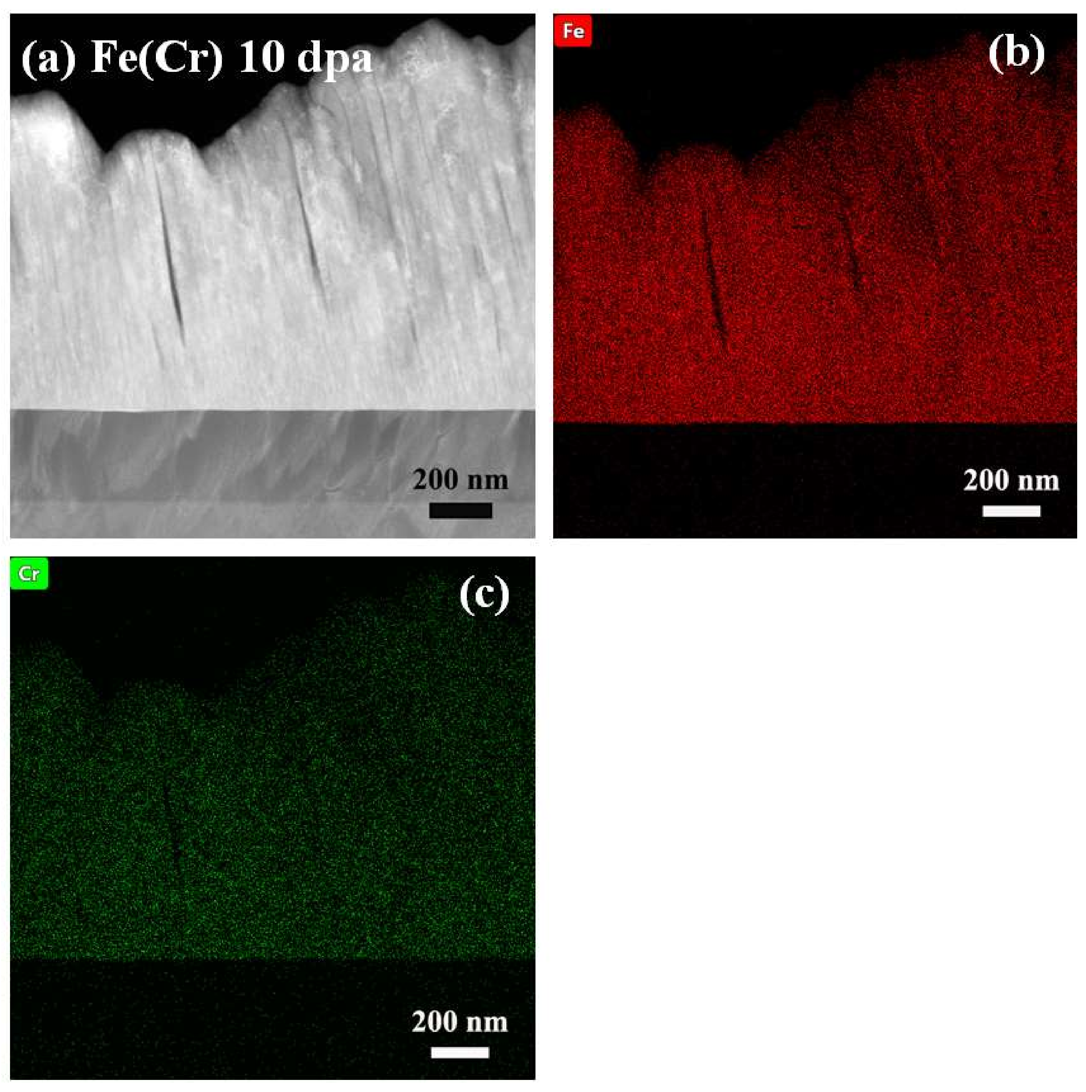
To examine the possibility of irradiation-induced compositional variations in the Fe(Cr) constituents, scanning transmission electron microscopy and energy-dispersive X-ray spectroscope (EDS) mapping was conducted for Fe(Cr) film after 10 dpa irradiation. As shown in Figure 5b,c, nearly uniform Fe and Cr signals were both obtained in the Fe(Cr) film. Although Cr enrichment via interstitials is suggested for Fe(Cr) alloy after RT irradiation [41,42], no obvious Cr segregation was observed near the grain boundaries. In addition, no α precipitate formation was resolved in this study. Both Cr segregation and α precipitate would be too tiny to be resolved by the present EDS study. Future study is warranted for detailed microstructural analysis and examination of high temperature irradiation response, especially at temperatures above 555 °C, when possible chemical reaction, Cr segregation, and α precipitate would occur [26].
5. Conclusions
In conclusion, we compared the dose-dependent radiation response of Fe(Cr) films with the Fe(Cr)/SiOC nanolayered composite system after room temperature irradiation to nominal damage levels of approximately 10, 20, and 50 dpa. By introducing crystalline/amorphous Fe(Cr)/SiOC interfaces, the irradiation-induced Fe(Cr) grain growth in the width direction of the Fe(Cr) layers of the Fe(Cr)/SiOC composite were ~50% less than that in stand-alone Fe(Cr) films. Because the irradiation-induced grain growth can be correlated with the defect concentration in the Fe(Cr) constituents, all these observations suggest that the Fe(Cr)/SiOC crystalline/amorphous interfaces act as efficient defect sinks, trapping mobile interstitials and therefore suppressing the irradiation-induced grain growth. In addition, there is less irradiation-induced grain growth for Fe(Cr) compared to pure unalloyed Fe in both the composite and non-composite case. The results indicate that Cr plays a major role in suppressing defect migration which supports previous MD modeling.
Author Contributions
Q.S. prepared all specimens and designed the experiment with M.N.; T.W. carried out Fe irradiation under the supervision of L.S.; Q.S. wrote the original draft of the paper and all authors discussed the results and commented on the manuscript.
Funding
This research was funded by DoE Office of Nuclear Energy, Nuclear Energy Enabling Technologies, award DE-NE0008415. This work was supported by the U.S. Department of Energy, Office of Nuclear Energy under DOE Idaho Operations Office Contract DE-AC07- 051D14517 as part of a Nuclear Science User Facilities experiment.
Acknowledgments
The research was performed in part in the Nebraska Nanoscale Facility: National Nanotechnology Coordinated Infrastructure and the Nebraska Center for Materials and Nanoscience, which are supported by the National Science Foundation under Award ECCS: 1542182, and the Nebraska Research Initiative. The authors thank J. Jie and H. Wang for their help with the EDS measurement.
Conflicts of Interest
The authors declare no conflicts of interest.
References
- Zinkle, S.J.; Was, G.S. Materials challenges in nuclear energy. Acta Mater. 2013, 61, 735–758. [Google Scholar] [CrossRef]
- Zinkle, S.J.; Terrani, K.A.; Snead, L.L. Motivation for utilizing new high-performance advanced materials in nuclear energy systems. Curr. Opin. Solid State Mater. Sci. 2016, 20, 401–410. [Google Scholar] [CrossRef]
- Odette, G.R.; Lucas, G.E. Embrittlement of nuclear reactor pressure vessels. JOM J. Miner. Met. Mater. Soc. 2001, 53, 18–22. [Google Scholar] [CrossRef]
- Odette, G.R.; Alinger, M.J.; Wirth, B.D. Recent developments in irradiation-resistant steels. Annu. Rev. Mater. Res. 2008, 38, 471–503. [Google Scholar] [CrossRef]
- Odette, G.R.; Hoelzer, D.T. Irradiation-tolerant Nanostructured Ferritic Alloys: Transforming Helium from a Liability to an Asset. JOM 2010, 62, 84–92. [Google Scholar] [CrossRef]
- Chen, D.; Wang, J.; Chen, T.Y.; Shao, L. Defect annihilation at grain boundaries in alpha-Fe. Sci. Rep. 2013, 3, 1450. [Google Scholar] [CrossRef] [PubMed]
- Singh, B.N. Effect of Grain-Size on Void Formation during High-Energy Electron-Irradiation of Austenitic Stainless-Steel. Philos. Mag. 1974, 29, 25–42. [Google Scholar] [CrossRef]
- Bai, X.M.; Voter, A.F.; Hoagland, R.G.; Nastasi, M.; Uberuaga, B.P. Efficient Annealing of Radiation Damage Near Grain Boundaries via Interstitial Emission. Science 2010, 327, 1631–1634. [Google Scholar] [CrossRef] [PubMed]
- Misra, A.; Demkowicz, M.J.; Zhang, X.; Hoagland, R.G. The radiation damage tolerance of ultra-high strength nanolayered composites. JOM 2007, 59, 62–65. [Google Scholar] [CrossRef]
- Soraru, G.D.; Suttor, D. High temperature stability of sol-gel-derived SiOC glasses. J. Sol-Gel Sci. Technol. 1999, 14, 69–74. [Google Scholar] [CrossRef]
- Soraru, G.D.; Dallapiccola, E.; DAndrea, G. Mechanical characterization of sol-gel-derived silicon oxycarbide glasses. J. Am. Ceram. Soc. 1996, 79, 2074–2080. [Google Scholar] [CrossRef]
- Harshe, R.; Balan, C.; Riedel, R. Amorphous Si(Al)OC ceramic from polysiloxanes: Bulk ceramic processing, crystallization behavior and applications. J. Eur. Ceram. Soc. 2004, 24, 3471–3482. [Google Scholar] [CrossRef]
- Rouxel, T.; Massouras, G.; Soraru, G.D. High temperature behavior of a gel-derived SiOC glass: Elasticity and viscosity. J. Sol-Gel Sci. Technol. 1999, 14, 87–94. [Google Scholar] [CrossRef]
- Nastasi, M.; Su, Q.; Price, L.; Colón Santana, J.A.; Chen, T.; Balerio, R.; Shao, L. Superior radiation tolerant materials: Amorphous silicon oxycarbide. J. Nucl. Mater. 2015, 461, 200–205. [Google Scholar] [CrossRef] [Green Version]
- Su, Q.; Cui, B.; Kirk, M.A.; Nastasi, M. Cascade effects on the irradiation stability of amorphous SiOC. Philos. Mag. Lett. 2016, 96, 60–66. [Google Scholar] [CrossRef]
- Su, Q.; Ding, H.P.; Price, L.; Shao, L.; Hinks, J.A.; Greaves, G.; Donnelly, S.E.; Demkowicz, M.J.; Nastasi, M. Rapid and damage-free outgassing of implanted helium from amorphous silicon oxycarbide. Sci. Rep. 2018, 8, 5009. [Google Scholar] [CrossRef] [Green Version]
- Su, Q.; Inoue, S.; Ishimaru, M.; Gigax, J.; Wang, T.Y.; Ding, H.P.; Demkowicz, M.J.; Shao, L.; Nastasi, M. Helium Irradiation and Implantation Effects on the Structure of Amorphous Silicon Oxycarbide. Sci. Rep. 2017, 7, 3900. [Google Scholar] [CrossRef]
- Di, Z.F.; Bai, X.M.; Wei, Q.M.; Won, J.; Hoagland, R.G.; Wang, Y.Q.; Misra, A.; Uberuaga, B.P.; Nastasi, M. Tunable helium bubble superlattice ordered by screw dislocation network. Phys. Rev. B 2011, 84, 052101. [Google Scholar] [CrossRef]
- Zhang, X.; Li, N.; Anderoglu, O.; Wang, H.; Swadener, J.G.; Hochbauer, T.; Misra, A.; Hoagland, R.G. Nanostructured Cu/Nb multilayers subjected to helium ion-irradiation. Nucl. Instrum. Methods B 2007, 261, 1129–1132. [Google Scholar] [CrossRef]
- Demkowicz, M.J.; Hoagland, R.G.; Hirth, J.P. Interface structure and radiation damage resistance in Cu-Nb multilayer nanocomposites. Phys. Rev. Lett. 2008, 100, 136102. [Google Scholar] [CrossRef]
- Su, Q.; Wang, T.Y.; Gigax, J.; Shao, L.; Nastasi, M. Resistance to Helium Bubble Formation in Amorphous SiOC/Crystalline Fe Nanocomposite. Materials 2019, 12, 93. [Google Scholar] [CrossRef]
- Madjasevic, M.; Alrriazouzi, A. Effect of Cr on the mechanical properties and microstructure of Fe-Cr model alloys after n-irradiation. J. Nucl. Mater. 2008, 377, 147–154. [Google Scholar] [CrossRef]
- Bhattacharya, A.; Meslin, E.; Henry, J.; Barbu, A.; Poissonnet, S.; Decamps, B. Effect of chromium on void swelling in ion irradiated high purity Fe-Cr alloys. Acta Mater. 2016, 108, 241–251. [Google Scholar] [CrossRef]
- Jenkins, M.L.; Yao, Z.; Hernandez-Mayoral, M.; Kirk, M.A. Dynamic observations of heavy-ion damage in Fe and Fe-Cr alloys. J. Nucl. Mater. 2009, 389, 197–202. [Google Scholar] [CrossRef]
- Horvath, J.; Uhlig, H.H. Critical Potentials for Pitting Corrosion of Ni Cr-Ni Cr-Fe and Related Stainless Steels. J. Electrochem. Soc. 1968, 115, 791–795. [Google Scholar] [CrossRef]
- Su, Q.; Zhernenkov, M.; Ding, H.; Price, L.; Haskel, D.; Watkins, E.B.; Majewski, J.; Shao, L.; Demkowicz, M.J.; Nastasi, M. Reaction of amorphous/crystalline SiOC/Fe interfaces by thermal annealing. Acta Mater. 2017, 135, 61–67. [Google Scholar] [CrossRef]
- Ziegler, J.F.; Biersack, J.P. The Stopping and Range of Ions in Solids; Pergamon Press: New York, NY, USA, 1985. [Google Scholar]
- Kaiser, N. Review of the fundamentals of thin-film growth. Appl. Opt. 2002, 41, 3053–3060. [Google Scholar] [CrossRef]
- Jenkins, M.L.; Kirk, M.A. Characterisation of Radiation Damage by Transmission Electron Microscopy; CRC Press, Taylor & Francis Group: Boca Raton, FL, USA, 2000. [Google Scholar]
- Liu, J.C.; Nastasi, M.; Mayer, J.W. Ion Irradiation Induced Grain-Growth in Pd Polycrystalline Thin-Films. J. Appl. Phys. 1987, 62, 423–428. [Google Scholar] [CrossRef]
- Liu, J.C.; Li, J.; Mayer, J.W. Temperature Effect on Ion-Irradiation-Induced Grain-Growth in Cu Thin-Films. J. Appl. Phys. 1990, 67, 2354–2358. [Google Scholar] [CrossRef]
- Atwater, H.A.; Thompson, C.V.; Smith, H.I. Ion-Bombardment-Enhanced Grain-Growth in Germanium, Silicon, and Gold Thin-Films. J. Appl. Phys. 1988, 64, 2337–2353. [Google Scholar] [CrossRef]
- Alexander, D.E.; Was, G.S.; Rehn, L.E. Ion-Induced Grain-Growth in Multilayer and Coevaporated Metal Alloy Thin-Films. Nucl. Instrum. Methods B 1991, 59, 462–466. [Google Scholar] [CrossRef]
- Kaoumi, D.; Motta, A.T.; Birtcher, R.C. A thermal spike model of grain growth under irradiation. J. Appl. Phys. 2008, 104, 073525. [Google Scholar] [CrossRef]
- Voegeli, W.; Albe, K.; Hahn, H. Simulation of grain growth in nanocrystalline nickel induced by ion irradiation. Nucl. Instrum. Methods B 2003, 202, 230–235. [Google Scholar] [CrossRef]
- Bacon, D.J.; Calder, A.F.; Gao, F.; Kapinos, V.G.; Wooding, S.J. Computer-Simulation of Defect Production by Displacement Cascades in Metals. Nucl. Instrum. Methods B 1995, 102, 37–46. [Google Scholar] [CrossRef]
- Zinkle, S.J.; Seitzman, L.E.; Wolfer, W.G. Stability of Vacancy Clusters in Metals.1. Energy Calculations for Pure Metals. Philos. Mag. A 1987, 55, 111–125. [Google Scholar] [CrossRef]
- Fu, C.C.; Dalla Torre, J.; Willaime, F.; Bocquet, J.L.; Barbu, A. Multiscale modelling of defect kinetics in irradiated iron. Nat. Mater. 2005, 4, 68–74. [Google Scholar] [CrossRef]
- Shim, J.-H.; Lee, H.-J.; Wirth, B.D. Molecular dynamics simulation of primary irradiation defect formation in Fe–10%Cr alloy. J. Nucl. Mater. 2006, 351, 56–64. [Google Scholar] [CrossRef]
- Terentyev, D.; Malerba, L.; Barashev, A.V. On the correlation between self-interstitial cluster diffusivity and irradiation-induced swelling in Fe-Cr alloys. Philos. Mag. Lett. 2005, 85, 587–594. [Google Scholar] [CrossRef]
- Wharry, J.P.; Was, G.S. The mechanism of radiation-induced segregation in ferritic-martensitic alloys. Acta Mater. 2014, 65, 42–55. [Google Scholar] [CrossRef]
- Senninger, O.; Soisson, F.; Martinez, E.; Nastar, M.; Fu, C.C.; Brechet, Y. Modeling radiation induced segregation in iron-chromium alloys. Acta Mater. 2016, 103, 1–11. [Google Scholar] [CrossRef]
Figure 1.
The cross-sectional TEM micrographs of as-deposited (a) Fe(Cr) and (b) Fe(Cr)/SiOC nanolayered films. Both stand-alone Fe(Cr) and Fe(Cr) layers in the nanolayered specimen exhibit a typical columnar growth with an average grain size of ~20 nm. The inset of (a) and (b) are an indexed selective area diffraction pattern showing the presence of a body-centered cubic (BCC) structure in Fe(Cr) and the amorphous nature of the SiOC layer. Clear interfaces are observed between Fe(Cr) and SiOC as seen in (c) and at high magnification in (d).

Figure 2.
The simulated depth profile of radiation damage and Fe concentration in (a) Fe(Cr) and (b) Fe(Cr)/SiOC nanolayered composite. (Values calculated using a dose of 1.54 × 10¹⁶ ions/cm2 for Fe(Cr) and 1.77 × 10¹⁶ ions/cm2 for Fe(Cr)/SiOC composite films).
Figure 2.
The simulated depth profile of radiation damage and Fe concentration in (a) Fe(Cr) and (b) Fe(Cr)/SiOC nanolayered composite. (Values calculated using a dose of 1.54 × 10¹⁶ ions/cm2 for Fe(Cr) and 1.77 × 10¹⁶ ions/cm2 for Fe(Cr)/SiOC composite films).

Figure 3.
Low magnification cross-sectional bright-field TEM micrographs of the Fe(Cr) films after (a) 10 dpa and (b) 50 dpa irradiation at room temperature. The microstructural evolution of the Fe(Cr)/SiOC nanolayered films after (c) 10 dpa and (d) 50 dpa irradiation. The irradiation damage (blue dash curve) and Fe concentration profile (red dash curve) are also overlaid on (b) Fe(Cr) and (d) Fe(Cr)/SiOC nanolayered films after 50 dpa irradiation. Grain growth is the main observation in both specimens. Typical examples identifying the grain size distribution in (e) Fe(Cr) and (f) Fe(Cr)/SiOC after 50 dpa irradiation.

Figure 4.
The average grain size in the width direction of the Fe(Cr) film and the Fe(Cr)/SiOC multilayer as a function of irradiation damage level. The rate of grain size increase for stand-alone Fe(Cr) films is greater than that of Fe(Cr) in the composite sample. Grain growth in the width direction of pure Fe films and Fe/SiOC nanolayered specimens after the same amount of irradiation is also included for comparison.

Figure 5.
(a) Scanning transmission electron microscopy image of the pure Fe(Cr) film after 10 dpa irradiation. The energy-dispersive X-ray spectroscope mapping result of (b) Fe and (c) Cr of this specimen. No obvious Cr enrichment was observed.
Figure 5.
(a) Scanning transmission electron microscopy image of the pure Fe(Cr) film after 10 dpa irradiation. The energy-dispersive X-ray spectroscope mapping result of (b) Fe and (c) Cr of this specimen. No obvious Cr enrichment was observed.

© 2019 by the authors. Licensee MDPI, Basel, Switzerland. This article is an open access article distributed under the terms and conditions of the Creative Commons Attribution (CC BY) license (http://creativecommons.org/licenses/by/4.0/).
Share and Cite
MDPI and ACS Style
Su, Q.; Wang, T.; Shao, L.; Nastasi, M. Radiation Tolerance in Nano-Structured Crystalline Fe(Cr)/Amorphous SiOC Composite. Crystals 2019, 9, 147. https://doi.org/10.3390/cryst9030147
AMA Style
Su Q, Wang T, Shao L, Nastasi M. Radiation Tolerance in Nano-Structured Crystalline Fe(Cr)/Amorphous SiOC Composite. Crystals. 2019; 9(3):147. https://doi.org/10.3390/cryst9030147
Chicago/Turabian StyleSu, Qing, Tianyao Wang, Lin Shao, and Michael Nastasi. 2019. "Radiation Tolerance in Nano-Structured Crystalline Fe(Cr)/Amorphous SiOC Composite" Crystals 9, no. 3: 147. https://doi.org/10.3390/cryst9030147
Note that from the first issue of 2016, this journal uses article numbers instead of page numbers. See further details here.