Preparation of Few-Layer Graphene by Pulsed Discharge in Graphite Micro-Flake Suspension
by
 , , ,
, , ,
Xin Gao
1,2 ,
,
Naoaki Yokota
2,
Hayato Oda
2,
Shigeru Tanaka
2,
Kazuyuki Hokamoto
2,
Pengwan Chen
1,* and
Meng Xu
3 1
State Key Laboratory of Explosion Science and Technology, Beijing Institute of Technology, Beijing 100081, China
2
Institute of Pulsed Power Science, Kumamoto University, Kumamoto 860-8555, Japan
3
School of Material Science and Engineering, Beijing Institute of Technology, Beijing 100081, China
*
Author to whom correspondence should be addressed.
Crystals 2019, 9(3), 150; https://doi.org/10.3390/cryst9030150
Submission received: 28 January 2019
/
Revised: 3 March 2019
/
Accepted: 8 March 2019
/
Published: 13 March 2019
(This article belongs to the Special Issue Graphene Mechanics)
Abstract
:Few-layer graphene nanosheets were produced by pulsed discharge in graphite micro-flake suspension at room temperature. In this study, the discharging current and voltage data were recorded for the analysis of the pulsed discharge processes. The as-prepared samples were recovered and characterized by various techniques, such as TEM, SEM, Raman, XRD, XPS, FT-IR, etc. The presence of few-layer graphene (3–9 L) in micrometer scale was confirmed. In addition, it is investigated that the size of recovered graphene nanosheets are influenced by the initial size of utilized graphite micro-flake powder. Based on the process of pulsed discharge and our experimental results, the formation mechanism of few-layer graphene was discussed. The influence of charging voltage on as-prepared samples is also investigated.
1. Introduction
Graphene is the first prepared two-dimensional material with a structure of single graphitic layer. Since Novoselov et al. [1] obtained monolayer graphene in millimeter-scale by mechanical exfoliation method with a tape in 2004, the synthesis and characterization of graphene materials have been an interest of many research groups. Various optical, electronic, thermal and mechanical properties of graphene were reported. In 2006, it was reported that, owing to the zigzag-shaped edge of graphene nano-ribbons, in-plane homogeneous electric fields can be loaded to control their magnetic properties and spin-polarized electronic state [2]. Moreover, graphene has been utilized to design and assemble multiple functional materials with excellent mechanical properties [3,4,5]. A significant amount of studies suggest the high potential applications of graphene materials in batteries, electronic devices, functional composite materials, etc. [6,7,8].
Various approaches for the preparation of graphene have been documented [9], such as the mechanical exfoliation method, oxidation reduction method, chemical vapor deposition (CVD) method, liquid-phase exfoliation method, arc-discharge method, electrochemical exfoliation method, detonation method, pulsed wire discharge method. Regarding the mechanical exfoliation method, graphene nanosheets with good crystallinity were obtained successfully using a tape to exfoliate highly-oriented pyrolytic graphite [1,10,11]. In the oxidation-reduction method, graphite oxide is firstly synthesized by oxidation of graphite for a larger gap between every two graphitic layers, then treated by ultrasonic dispersion or thermal expansion to obtain graphene oxide for further reduction to form graphene [12,13]. With respect to the CVD method, certain hydrocarbon gases are decomposed at high temperatures, causing free carbon atoms to deposit on certain substrates to form graphene films [14,15,16]. The liquid-phase exfoliation method employs ultrasonic dispersion treatment and the cavitation effect to exfoliate the graphite powder in liquid medium [17]. Graphene can also be synthesized along the process of arc-discharge method. In this method, a direct and self-sustained arc-discharge between two graphite electrodes produces and forces the carbon atoms to deposit on the inner surface of recovery container to form graphene [18]. Otherwise, Liu et al. [19] and Rao et al. [20] reported the preparation of graphene from the electrochemical exfoliation of graphite electrode. In this method, two graphite electrodes are immersed in ionic liquid and a static potential is applied for the oxidation and expansion of graphitic layers, resulting in the exfoliation of graphitic layers [19]. Recently, Chen et al. [21,22] synthesized graphene materials through detonation method using detonation and shock waves to produce carbon atoms which deposited on certain metal surfaces to form graphene.
Pulsed discharge refers to when a strong current passes through the medium between two electrodes, a high-density energy is injected into the medium, leading to a rapid temperature increase, phase transition, rapid expansion, flash, etc. Using different mediums in the experiments, this technique has been utilized in multiple studies, such as pulsed wire discharge, liquid pulsed discharge, etc. Pulsed wire discharge (electrical wire explosion) refers to a conductive wire fixed between two electrodes melts and vaporizes during pulsed discharge, resulting in an explosion with high temperature and inner pressure [23,24]. The pulsed wire discharge method has been widely applied to synthesize nanomaterials. Liquid pulsed discharge refers to the phenomenon that the liquid medium between two electrodes breaks down because of the pulsed discharge, leading to the formation of strong plasma tunnel at high temperature and inner pressure. The generated atoms and ions burst into medium with a strong shockwave and cavitation bubble collapse subsequently [25,26]. Liquid pulsed discharge is utilized for degradation of organic [27,28], cell sterilization [29] in water and other applications [30,31].
In our previous studies, graphene materials were prepared by the pulsed wire discharge method [23], in which a graphite stick connected to electrodes starts to melt and expand due to the joule heating of pulsed discharge at a high temperature and inner pressure and then the graphitic layers in the stick overcome the Van der Waals force to form graphene during the subsequent explosion in a distilled water medium. Furthermore, Rud et al. [32] synthesized nano amorphous carbon with diamond-like short-range order using ionization and deposition induced by pulsed discharge in organic liquids, showing its potential of synthesizing nanomaterials. In this work, we demonstrate a one-step route to prepare few-layer graphene using pulsed discharge in graphite micro-flake suspension at room temperature.
2. Materials and Methods
In the experiments, we used a cylindrical stainless chamber with an inner diameter of 200 mm and a depth of 400 mm to contain liquid medium and recover the samples (Figure 1). A transparent polypropylene pipe (20 mm in inner diameter, 24 mm in outer diameter and 30 mm length) with two insulation blocks was utilized to contain graphite micro-flake suspension. The graphite micro-flake suspension (1 g∙L−1) was prepared by mixing distilled water and graphite micro-flake powder in different sizes (~10 μm, ~30 μm and ~300 μm mesh as listed in Table 1), respectively, to investigate the influence of graphite micro-flake size on as-prepared samples. Two pure iron electrodes with a tip-point were fixed to the insulation blocks along the axis and spaced an invariant 2 mm apart in the pipe. Then, the pipe containing graphite micro-flake suspension and electrodes was placed in the middle of the stainless chamber filled with approximate 500 mL distilled water. Then the two electrodes were connected to a 12.5 μF capacitor. Two charging voltages (30 kV and 40 kV as listed in Table 1) were selected for discharge.
After discharge, the recovered suspensions were collected in beakers, centrifuged and filtered to remove the unexfoliated graphite nanosheets. Then the suspensions were purified by HCl to remove the trace amount of iron or iron oxide nanoparticles from iron electrodes. Subsequently, the samples were separated and dried using a freeze dryer for further characterization.
High resolution transmission electron microscope (TEM) images and field emission scanning electron microscope (SEM) images were obtained using FEI Tecnai G2 F20 S-Twin (FEI, Hillsboro, OR, USA) and Hitachi S-4800 (Hitachi, Tokyo, Japan) to examine the microstructure and morphology of recovered samples at working accelerating voltages of 200 kV and 10 kV, respectively. The Raman spectra of samples were obtained using Raman spectrometer (LabRAM Aramis, HORIBA Scientific, Kyoto, Japan) equipped with a He-Ne laser (633 nm) for carbon phase analysis. An X-ray diffractometer (XRD) (X pert pro MPD) with CuKα radiation (k = 0.15406 nm) was utilized to record XRD patterns at a working voltage and current of 40 kV and 200 mA, respectively, and a step size of 0.0330° (2θ). Fourier transform infrared (FT-IR) spectra were recorded on a Thermo iZ10 FT-IR spectroscopy (Thermo Fisher Scientific, Waltham, MA, USA) using KBr discs.
3. Results
The detailed experimental conditions are listed in Table 1. The charging voltage was 30 kV for samples Nos. 1, 3 and 4 and 40 kV for sample No. 2, respectively. The main phase of recovered samples identified by SEM, TEM and Raman spectroscopy was identified to be few-layer graphene.
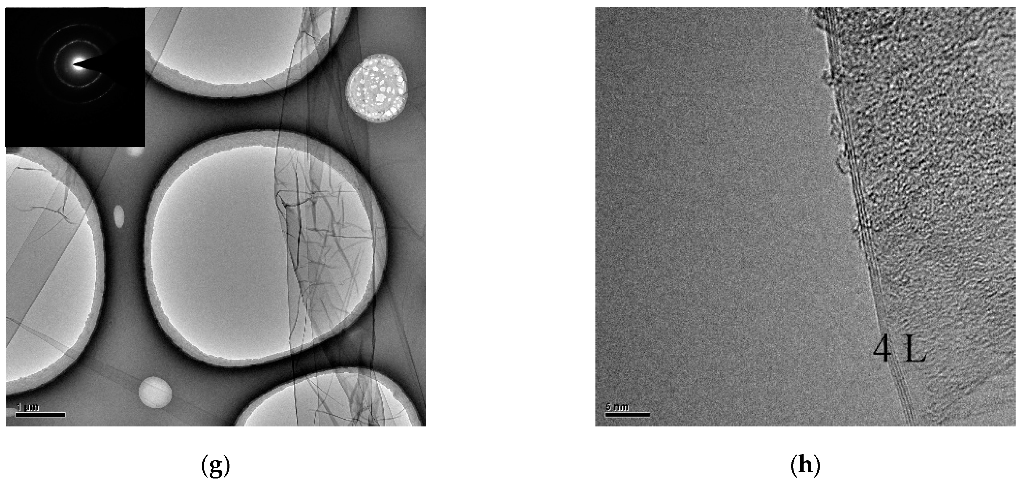
Typical TEM images of recovered samples (Figure 2) shows the presence of loose and extended ultra-thin carbon nanosheets with interlayer distances of 0.3–0.4 nm at the edges, which are in good agreement with the morphology and microstructure of few-layer graphene [21,23,33]. The high resolution TEM images (Figure 2b,d,f,h) further reveal that the graphitic layer number of the few-layer graphene is in the range of 3–9 (as listed in Table 1), indicating that the main content of purified recovered samples is few-layer graphene. The selected area electron diffraction (SAED) patterns (the inset images of Figure 2a,c,e,g) indicate a ring-like diffraction with dispersed bright spots. The same results were observed in few-layer [21,23] graphene, resulting from rotational staking faults in the matrix graphene sheets.
Figure 3 presents the typical SEM images of ultra-thin carbon nanosheets in the recovered samples, revealing the presence of the typical morphology of few-layer grapheme [23,34], which are curved, loose and extended to micrometer scale. The curly and wrinkled structure of observed carbon films is owing to the thermodynamic instability of the two-dimensional material [35]. Furthermore, the statistics of graphene nanosheets in over 20 SEM images of each recovered sample shows that the nanosheet size became larger as the larger of graphite flake powder used in the experiments. When the graphite micro-flake powders are in the size of ~10 μm mesh (Nos. 1 and 2), the sizes of observed graphene nanosheets (Figure 3a,c) are in the range of 0.5–10 μm. While the graphite flake powders are in the size of ~30 μm mesh (No. 3), the sizes of observed graphene nanosheets (Figure 3e) increase to the range of 15–25 μm. As the graphite flakes with ~300 μm mesh is used for experiment (No. 4), the sizes of observed graphene nanosheets (Figure 3g) are larger than 100 μm mostly. The observation suggests a positive correlation between the size of initial graphite micro-flake and the size of as-prepared graphene nanosheet. It implies that the nature formation mechanism of graphene is exfoliation of graphitic layers from the raw materials.
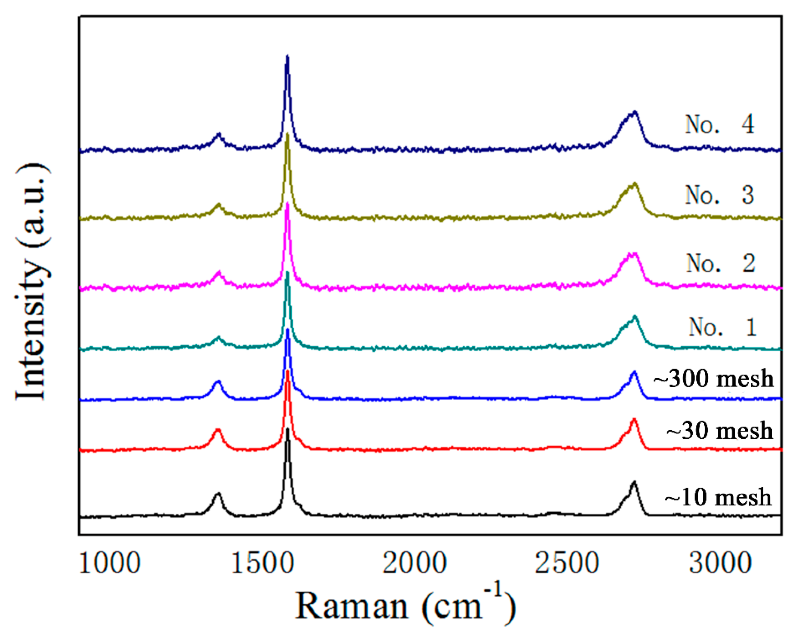
Raman spectroscopy is very informative and sensitive for studying carbon materials [36]. It provides a quick and facile identification of carbon materials [21,23,37,38], which is a significant method to identify graphene. As shown in Figure 4, three characteristic bands are observed in each Raman spectrum, including D band (approximate 1340 cm−1), G band (approximate 1580 cm−1) and 2D band (approximate 2660 cm−1).
The 2D band and the intensity ratio of 2D band to G band (I2D/IG) have been utilized to identify mono-layer graphene and few-layer graphene from other carbon materials universally [37,39]. A higher I2D/IG indicates less graphitic layers [23,33] in the graphene nanosheets. As listed in Table 1, the I2D/IG of recovered samples are in the range of 1.32–1.44, which are much larger than those of raw graphite flakes (0.76–0.86), indicating the presence of few-layer graphene in the recovered samples [23,33,40]. Furthermore, the intensity ratio of D band to G band (ID/IG) features the disorder of graphene nanosheets and is utilized to estimate disorder degree on graphitic layers [34,37]. Note that the ID/IG of Sample No. 2 (0.40) is greater than those of Sample Nos. 1, 3 and 4 (0.25–0.33), indicating higher disorder degree of graphene nanosheets in Sample No. 2 [20], which is believed to be caused by higher energy input with the charging voltage of 40 kV. While the ID/IG of all recovered samples (0.25–0.40) are close to those of raw graphite flakes (0.42–0.46), suggesting their good crystallinity compared with the graphene prepared by oxidation-reduction method (ID/IG = ~1) [12]. The Raman spectra result may present the influence of charging voltage on the disorder degree in the recovered samples.
XRD pattern is an auxiliary method to characterize the crystallinity and thickness of graphene samples [41]. In XRD patterns of as-prepared samples (Figure 5), one obvious characteristic peak appears in the 26.1–26.3° range assigned to graphene (and graphite) (002) diffraction [21,42,43]. The calculated corresponding lattice distances are in a range of 3.39–3.41 Å, which are slightly larger than that of graphite (3.35 Å) [21]. It is also in good agreement with the TEM measurements. Furthermore, the weaker peaks with higher FWHM values (as shown in inset of Figure 5) demonstrate the non-uniform multilayer distribution of ultra-thin few-layer graphene [44,45], supporting the observation results of TEM images.
Figure 6 shows the XPS results of Sample Nos. 1 and 2, in which all the curves were fitted on the basis of Shirley background correlation and using Gaussian-Lorentzian peak shape. The C1s spectrum of Sample No. 1 in Figure 6a can be fitted to the mainly non-oxygenated C in aromatic rings (C=C/C–C, 284.8 eV) and the C in oxygen-containing functional groups (C–OH, 286.3 eV) [46,47]. While the C1s spectrum of Sample No. 2 can be fitted to the mainly non-oxygenated C in aromatic rings (C=C/C–C, 284.3 eV) and the C in multiple oxygen-containing functional groups, such as C–O (285.6eV), C–OH (286.6 eV), C=O (288.4eV) and O–C=O (289.9 eV) [48,49]. It reveals a higher content of oxygen-containing groups in Sample No. 2. The binding energy peaks observed in both C1s spectra indicate the reaction between graphitic layer and the oxygen produced by discharge plasma during the breakdown process. The multiple binding energy peaks of C and O in Sample No. 2 with higher intensities may result from the higher stored energy controlled by higher charging voltage.
FT-IR spectra (Figure 7) reveals that as-prepared graphene in Sample Nos. 1 and 2 presents multiple absorption peaks of various chemical bonds. The strongest peak in both spectra, set at approximately 3445 cm−1, is indicative of ubiquitous O-H stretches [50,51,52]. Besides, both spectra present several peculiar absorption peaks at 2875–2957 cm−1 (symmetric and anti-symmetric stretching vibrations of CH2) [51,52], at approximately 1629 and 1440 cm−1 (C=C, skeletal vibrations of unoxidized graphitic domains) [51,53], at approximately 1387 cm−1 (the stretching vibration of C–O of carboxylic acid) [52] and at 1053 cm−1 (alkoxy C–O stretching vibration) [52,53,54]. Furthermore, in FT-IR spectrum of Sample No. 2, two other peaks are observed at 1250 cm−1 and 1160 cm−1, which are assigned to stretching vibration of epoxy C–O–C [52,54] and different alcoholic C–OH [50], respectively. As for Sample No. 2, a dramatic intensity increase of absorption peaks related to oxygen-containing functional groups and the presence of peaks appearing at 1250 and 1160 cm−1 indicate the increase of oxygenated groups on graphene nanosheets [54].
4. Discussion
Figure 8 shows typical discharge current and voltage curves of liquid pulsed discharge experiments, consisting of two processes (pre-breakdown and breakdown). According to previous studies [25,26,55], the pre-breakdown process during the beginning few microseconds reveals that the discharge voltage descends gradually from the values of charging voltage while the discharge current oscillates at a low value. Meanwhile, the strong electric field between two electrodes induces the ionization of the water molecules. The subsequent breakdown process, in which the suspension between two electrodes breaks down to generate a strong plasma tunnel, features the typical damped cosine-wave discharge voltage after a rapid decrease and a damped sine-wave discharge current [25,26]. Following this, the ions and atoms (H, O, OH−, etc.) in the plasma at high temperature and high inner pressure burst out to generate shock waves (101–103 MPa) [25,55] and the formation of cavitation bubbles [56,57]. Furthermore, Figure 8 shows an obvious influence of charging voltage on the discharge voltage and current curves. At the ascent of charging voltage, the pre-breakdown duration becomes shorter and the discharge current during the breakdown process becomes stronger, indicating stronger plasma and shock waves. This phenomenon is in a good agreement with the typical law of liquid pulsed discharge [25]. Because of the stronger plasma, more oxidizer was produced and reacted with exfoliated few-layer graphene, leading to the higher oxidation degree and disorder degree of the few-layer graphene. It is coincident with the results of Raman spectra and XPS spectra. In addition, by measuring the mass of graphite micro-flakes before mixing and the purified recovered graphene, the calculated yields of graphene prepared via pulsed discharge are in 20–30% range, as listed in Table 1. Among them, the yield of Sample No. 2 is higher than others, implying that higher injected energy with stronger shockwave leads to a higher productivity.
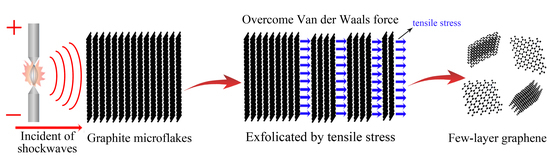
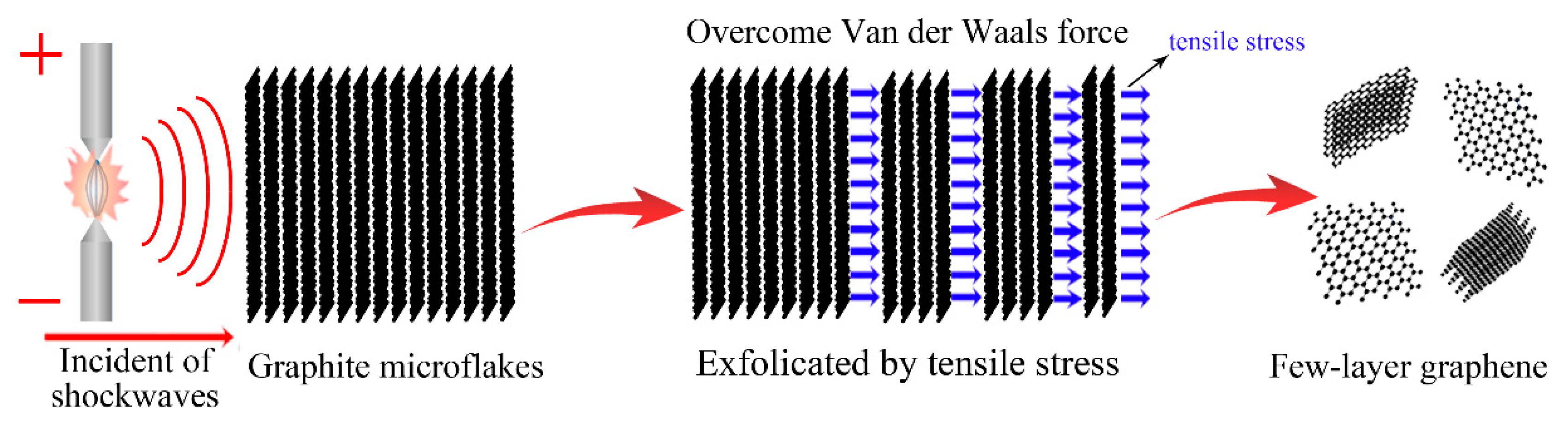
Based on the above results and analysis, we carefully propose the following mechanism regarding the formation of few-layer graphene using liquid pulsed discharge (as shown in Figure 8). During the breakdown process of the liquid pulsed discharge, the generated ions and atoms at high temperatures and pressures burst out with the generation of shock waves and cavitation bubbles. The cavitation bubbles collapse and also generate shock waves and micro-jets [57,58]. As the generated shock waves (with pressures of over hundreds of MPa) [57] impact on graphite micro-flakes, transmitted shock waves are formed and propagate in graphite micro-flakes. Subsequently, the transmitted waves propagate to the graphite-water interface to form the reflected rarefaction waves in graphite due to a huge mismatch between the acoustic impedances of graphite (approximately 6000–8000 Pa∙s∙m−1) and water (approximately 1500 Pa∙s∙m−1) [59,60,61]. When the superposed stress in graphite micro-flakes are tensile stress, the graphitic layers in the micro-flakes are easily exfoliated to form few-layer graphene and spread out in water because of the weak Van der Waals force between graphitic layers (Figure 9). In addition, the cavitation-induced micro-jets also act on the graphite surfaces [58], leading to a shear effect to exfoliate graphitic layers.
However, these exfoliation forces acting on the graphite powder to overcome the graphitic layer interactions are not strong enough to cause the molecular destruction in graphitic layer, implying that the size of recovered graphene nanosheets depends on the size of graphite flake powders, which is in good agreement with the size of recovered samples. Furthermore, when the charging voltage is higher, more energy is injected into plasma tunnel, leading to stronger generated shockwaves and stronger superimposed tensile tress. Under this situation, the exfoliation efficiency is higher, resulting in that the yield of Sample No. 2 (40 kV) is larger than those of Sample No. 1, 3 and 4 (30 kV), as listed in Table 1.
5. Conclusions
In summary, few-layer graphene has been obtained by pulsed discharge in graphite micro-flake suspension. Under the action of shock waves induced by pulsed discharge, the graphitic layers in graphite micro-flake powders are exfoliated to form few-layer graphene (3–9 L). The charging voltage influences not only the crystallinity but also the yield of as-prepared graphene. When the charging voltage is higher (40 kV), ID/IG from Raman spectra rises up from 0.25 to 0.40, indicating a higher disorder degree and the measured yield increase from ~20% to ~30%. Furthermore, it is also investigated that the size of recovered graphene nanosheets is influenced by the initial size of graphite micro-flake powders utilized in experiments.
Author Contributions
P.C., X.G. and K.H. conceived and designed the above experiments; X.G., S.T., N.Y. and H.O. performed the experiments and recorded the experimental data; X.G., S.T. and M.X. analyzed the data; S.T., K.H., M.X. and P.C. contributed reagents/materials/analysis tools; X.G. and P.C. wrote the paper.
Funding
This research was funded by the Project of State Key Laboratory of Explosion Science and Technology, Beijing Institute of Technology, grant number ZDKT18-01.
Conflicts of Interest
The authors declare no conflict of interest. The funders had no role in the design of the study; in the collection, analyses, or interpretation of data; in the writing of the manuscript, or in the decision to publish the results.
References
- Novoselov, K.S.; Geim, A.K.; Morozov, S.V.; Jiang, D.; Zhang, Y.; Dubonos, S.V.; Grigorieva, I.V.; Firsov, A.A. Electric Field Effect in Atomically Thin Carbon Films. Science 2004, 306, 666–669. [Google Scholar] [CrossRef] [PubMed] [Green Version]
- Son, Y.W.; Cohen, M.L.; Louie, S.G. Half-Metallic Graphene Nanoribbons. Nature 2006, 444, 347–349. [Google Scholar] [CrossRef]
- Cao, J.; Zhang, Y.Y.; Men, C.L.; Sun, Y.Y.; Wang, Z.N.; Zhang, X.T.; Li, Q.W. Programmable Writing of Graphene Oxide/Reduced Graphene Oxide Fibers for Sensible Networks with in Situ Welded Junctions. ACS Nano 2014, 8, 4325–4333. [Google Scholar] [CrossRef]
- Huang, H.; Chen, P.W.; Zhang, X.T.; Lu, Y.; Zhan, W.C. Edge-to-Edge Assembled Graphene Oxide Aerogels with Outstanding Mechanical Performance and Superhigh Chemical Activity. Small 2013, 9, 1397–1404. [Google Scholar] [CrossRef]
- Rao, C.N.R.; Sood, A.K.; Subrahmanyam, K.S.; Govindaraj, A. Graphene: The New Two-Dimensional Nanomaterial. Angew. Chem. Int. Ed. 2009, 48, 7752–7777. [Google Scholar] [CrossRef] [PubMed]
- Lee, C.; Wei, X.; Kysar, J.; Hone, J. Measurement of The Elastic Properties and Intrinsic Strength of Monolayer Graphene. Science 2008, 321, 385–388. [Google Scholar] [CrossRef] [PubMed]
- Kroto, H.W.; Heath, J.R.; Obrien, S.C.; Curl, R.F.; Smalley, R.E. C60: Buckminsterfullerene. Nature 1985, 318, 162–163. [Google Scholar] [CrossRef]
- Li, G.Y.; Zhang, X.T.; Wang, J.; Fang, J.H. From Anisotropic Graphene Aerogels to Electron- and Photo-Driven Phase Change Composites. J. Mater. Chem. 2016, 4, 17042–17049. [Google Scholar] [CrossRef]
- Izhar, K.M.; Sebastian, D.; Izni, K.N.; Suriani, A.B.; Brigitte, V.; Rahman, M.A. Toward high production of graphene flakes—A Review on Recent Developments in Their Synthesis Methods and Scalability. J. Mater. Chem. A 2018, 6, 15010–15026. [Google Scholar]
- Pang, S.P.; Englet, J.M.; Tsao, H.N.; Hernandez, T.; Hirsch, A.; Feng, X.L.; Mullen, K. Extrinsic Corrugation-Assisted Mechanical Exfoliation of Monolayer Graphene. Adv. Mater. 2010, 22, 5374–5377. [Google Scholar] [CrossRef] [PubMed]
- You, M.C.; Kim, H.; Ju, H.L.; Song, Y.W. Multilayered Graphene Efficiently Formed by Mechanical Exfoliation for Nonlinear Saturable Absorbers in Fiber Mode-Locked Lasers. Appl. Phys. Lett. 2010, 97, 211102. [Google Scholar]
- Jiang, M.; Wu, J.; Ren, Z.; Qi, M.; Bai, J.; Bai, Y.; Zhang, Y.; Wang, Q. Synthesis of Graphene and Its Application as Wide-Band Saturable Absorbers. Nanotechnology 2012, 7, 1–4. [Google Scholar]
- Li, D.; Muller, M.B.; Gilje, S.; Kaner, R.B.; Wallace, G.G. Processable Aqueous Dispersions of Graphene Nanosheets. Nature 2008, 3, 101–105. [Google Scholar] [CrossRef]
- Gautam, M.; Jayatissa, A.H. Graphene Based Field Effect Transistor for The Detection of Ammonia. J. Appl. Phys. 2012, 112, 064304. [Google Scholar] [CrossRef]
- Reina, A.; Jia, X.T.; Ho, J.; Nezich, D.; Son, H.B.; Bulovic, V.; Dresselhaus, M.S.; Kong, J. Large Area, Few-Laye r Graphene Films on Arbitrary Substrates by Chemical Vapor Deposition. Nano. Lett. 2009, 9, 30–35. [Google Scholar] [CrossRef] [PubMed]
- Chen, X.P.; Zhang, L.L.; Chen, S.S. Large Area CVD Growth of Graphene. Synth. Met. 2015, 210, 95–108. [Google Scholar] [CrossRef]
- Hernandez, Y.; Nicolosi, V.; Lotya, M.; Blighe, F.M.; Sun, Z.Y.; De, S.; McGovern, I.T.; Holland, B.; Byrne, M.; Gun’ko, Y.K.; et al. High-Yield Production of Graphene by Liquid-Phase Exfoliation of Graphite. Nat. Nanotechnol. 2008, 3, 563–568. [Google Scholar] [CrossRef] [PubMed]
- Subrahmanyam, K.S.; Panchakarla, L.S.; Govindaraj, A.; Rao, C.N.R. Simple Method of Preparing Graphene Flakes by an Arc-Discharge Method. J. Phys. Chem. C 2009, 113, 4257–4259. [Google Scholar] [CrossRef]
- Liu, N.; Luo, F.; Wu, H.X.; Liu, Y.H.; Zhang, C.; Chen, J. One-Step Ionic-Liquid-Assisted Electrochemical Synthesis of Ionic-Liquid-Functionalized Graphene Sheets Directly from Graphite. Adv. Funct. Mater. 2008, 18, 1518–1525. [Google Scholar] [CrossRef]
- Rao, K.S.; Senthilnathan, J.; Liu, Y.F.; Yoshimura, M. Role of Peroxide Ions in Formation of Graphene Nanosheets by Electrochemical Exfoliation of Graphite. Sci. Rep.-UK 2014, 4, 4237. [Google Scholar] [CrossRef] [Green Version]
- Yin, H.; Chen, P.W.; Xu, C.X.; Gao, X.; Zhou, Q.; Zhao, Y.; Qu, L.T. Shock-Wave Synthesis of Multilayer Graphene and Nitrogen-Doped Graphene Materials from Carbonate. Carbon 2015, 94, 928–935. [Google Scholar] [CrossRef]
- Chen, P.W.; Xu, C.X.; Yin, H.; Gao, X.; Qu, L.T. Shock Induced Conversion of Carbon Dioxide to Few Layer Graphene. Carbon 2017, 115, 471–476. [Google Scholar] [CrossRef]
- Gao, X.; Xu, C.X.; Yin, H.; Wang, X.G.; Song, Q.Z.; Chen, P.W. Preparation of Graphene by Electrical Explosion of Graphite Sticks. Nanoscale 2017, 9, 10639–10646. [Google Scholar] [CrossRef] [PubMed]
- Gao, X.; Yokota, N.; Oda, H.; Tanaka, S.; Hokamoto, K.; Chen, P.W. One Step Preparation of Fe–FeO–Graphene Nanocomposite through Pulsed Wire Discharge. Crystals 2018, 8, 104. [Google Scholar] [CrossRef]
- Yan, D.; Bian, D.C.; Zhao, J.C.; Niu, S.Q. Study of the Electrical Characteristics, Shock-Wave Pressure Characteristics, and Attenuation Law Based on Pulse Discharge in Water. Shock Vib. 2016, 2016, 6412309. [Google Scholar] [CrossRef]
- Zhang, C.H.; Namihira, T.; Kiyan, T.; Nakashima, K.; Katsuki, S.; Akiyama, H.; Ito, H.; Imaizumi, Y. Investigation of Shockwave Produced by Large Volume Pulsed Discharge under Water. In Proceedings of the IEEE Pulsed Power Conference, Monterey, CA, USA, 13–15 June 2005; pp. 1377–1380. [Google Scholar]
- Li, J.; Sato, M.; Ohshima, T. Degradation of Phenol in Water Using A Gas-Liquid Phase Pulsed Discharge Plasma Reactor. Thin Solid Film. 2007, 515, 4283–4288. [Google Scholar] [CrossRef]
- Sugiarto, A.T.; Ito, S.; Ohshima, T.; Sato, M.; Skalny, J.D. Oxidative Decoloration of Dyes by Pulsed Discharge Plasma in Water. J. Electrostat. 2003, 58, 135–145. [Google Scholar] [CrossRef]
- Sato, M. Environmental and Biotechnological Applications of High-Voltage Pulsed Discharges in Water. Plasma Sources Sci. Technol. 2008, 17, 024021. [Google Scholar] [CrossRef]
- Sunka, P. Pulse Electrical Discharges in Water and Their Applications. Physis. Plasmas 2001, 8, 2587–2594. [Google Scholar] [CrossRef]
- Ihara, S.; Yamabe, C. Breaking of Ice Using Pulsed Power. Jpn. J. Appl. Phys. 2004, 43, 5528–5532. [Google Scholar] [CrossRef]
- Rud, A.D.; Kuskova, N.I.; Ivaschuk, L.I.; Zelinskaya, G.M.; Biliy, N.M. Structure State of Carbon Nanomaterials Produced by High-Energy Electric Discharge Techniques. Fuller. Nanotubes Carbon Nanostruct. 2011, 19, 120–126. [Google Scholar] [CrossRef]
- Gayathri, S.; Jayabal, P.; Kottaisamy, M.; Ramakrishnan, V. Synthesis of Few Layer Graphene by Direct Exfoliation of Graphite and A Raman Spectroscopic Study. AIP Adv. 2014, 4, 027116. [Google Scholar] [CrossRef]
- Zhu, L.X.; Zhao, X.; Li, Y.Z.; Yu, X.Y.; Li, C.; Zhang, Q.H. High-Quality Production of Graphene by Liquid-Phase Exfoliation of Expanded Graphite. Mater. Chem. Phys. 2013, 137, 984–990. [Google Scholar] [CrossRef]
- Shen, B.S.; Ding, J.J.; Yan, X.B.; Feng, W.J.; Li, J.; Xue, Q.J. Influence of Different Buffer Gases on Synthesis of Few-Layered Graphene by Arc Discharge Method. Appl. Surf. Sci. 2012, 258, 4523–4531. [Google Scholar] [CrossRef]
- Voronov, O.A.; Street, K.W., Jr. Raman Scattering in a New Carbon Material. Diam. Relat. Mater. 2010, 19, 31–39. [Google Scholar] [CrossRef]
- Malard, L.M.; Pimenta, M.A.; Dresselhaus, G.; Dresselhaus, M.S. Raman Spectroscopy in Graphene. Phys. Rep. 2009, 473, 51–87. [Google Scholar] [CrossRef]
- Kim, M.S.; Woo, J.M.; Geum, D.M.; Rani, J.R.; Jang, J.H. Effect of Copper Surface Pre-Treatment on The Properties of CVD Grown Graphene. AIP Adv. 2014, 4, 127107. [Google Scholar] [CrossRef]
- Eckmann, A.; Felten, A.; Mishchenko, A.; Britnell, L.; Krupke, R.; Novoselov, K.S.; Casiraghi, C. Probing The Nature of Defects in Graphene by Raman Spectroscopy. Nano Lett. 2012, 12, 3925–3930. [Google Scholar] [CrossRef]
- Tian, J.J.; Hu, B.S.; Wei, Z.D.; Jin, Y.; Luo, Z.T.; Xia, M.R.; Pan, Q.J.; Liu, Y.L. Surface Structure Deduced Differences of Copper Foil and Film for Graphene CVD Growth. Appl. Surf. Sci. 2014, 300, 73–79. [Google Scholar] [CrossRef]
- Saikia, B.K.; Boruah, R.K.; Gogoi, P.K. A X-Ray Diffraction Analysis on Graphene Layers of Assam Coal. J. Chem. Sci. 2009, 121, 103–106. [Google Scholar] [CrossRef]
- Mohammed, M.; Li, Z.R.; Cui, J.B.; Chen, T.P. Junction Investigation of Graphene/Silicon Schottky Diodes. Nanoscale Res. Lett. 2012, 7, 302. [Google Scholar] [CrossRef] [PubMed]
- Sheng, Z.H.; Chen, J.J.; Bo, W.J.; Wang, F.B.; Xia, X.H. Catalyst-Free Synthesis of Nitrogen-Doped Graphene via Thermal Annealing Graphite Oxide with Melamine and Its Excellent Electrocatalysis. ACS Nano 2011, 5, 4350–4358. [Google Scholar] [CrossRef] [PubMed]
- Andonovic, B.; Ademi, A.; Grozdanov, A.; Paunović, P.; Dimitrov, A.T. Enhanced Model for Determining The Number of Graphene Layers and Their Distribution from X-Ray Diffraction Data. Beilstein J. Nanotechnol. 2015, 6, 2113–2122. [Google Scholar] [CrossRef] [PubMed]
- Andonovic, B.; Grozdanov, A.; Paunović, P.; Dimitrov, A.T. X-Ray Diffraction Analysis on Layers in Graphene Samples Obtained by Electrolysis in Molten Salts: A New Perspective. Micro Nano Lett. 2015, 10, 683–685. [Google Scholar] [CrossRef]
- Mattevi, C.; Eda, G.; Agnoli, S.; Miller, S.; Mkhoyan, K.A.; Celik, O.; Mastrogiovanni, D.; Granozzi, G.; Garfunkel, E.; Chhowalla, M. Evolution of Electrical, Chemical, and Structural Properties of Transparent and Conducting Chemically Derived Graphene Thin Films. Adv. Funct. Mater. 2009, 19, 2577–2583. [Google Scholar] [CrossRef]
- Bagri, A.; Mattevi, C.; Acik, M.; Chabal, Y.J.; Chhovalla, M.; Shenoy, V.B. Structural Evolution during the Reduction of Chemically Derived Graphene Oxide. Nat. Chem. 2010, 2, 581–587. [Google Scholar] [CrossRef] [PubMed]
- Yang, D.X.; Velamakanni, A.; Bozuklu, G.; Park, S.; Stoller, M.; Piner, R.D.; Stankovich, S.; Jung, I.; Field, D.A.; Ventrice, C.A., Jr.; et al. Chemical Analysis of Graphene Oxide Films after Heat and Chemical Treatments by X-Ray Photoelectron. Carbon 2009, 47, 145–152. [Google Scholar] [CrossRef]
- Paredes, J.I.; Villar-Rodil, S.; Martinez-Alonso, A.; Tascon, J.M.D. Graphene Oxide Dispersions in Organic Solvents. Langmuir 2008, 24, 10560–10564. [Google Scholar] [CrossRef]
- Arrais, A.; Boccaleri, E.; Diana, E. Efficient Direct Water-Solubilisation of Single-Walled Carbon Nanotube Derivatives. Fuller. Nanotubes Carbon Nanostruct. 2004, 12, 789–809. [Google Scholar] [CrossRef]
- Arrais, A.; Diana, E.; Boccaleri, E. A Study on the Carbon Soot Derived from the Wood Combustion and on the Relative Alkali-Extractable Fraction. J. Mater. Sci. 2006, 41, 6036–6045. [Google Scholar] [CrossRef]
- Zhang, Y.P.; Pan, C.X. TiO2/Graphene Composite from Thermal Reaction of Graphene Oxide and Its Photocatalytic Activity in Visible Light. J. Mater. Sci. 2011, 46, 2622–2626. [Google Scholar] [CrossRef]
- Guo, H.L.; Wang, X.F.; Qian, Q.Y.; Wang, F.B.; Xia, X.H. A Green Approach to the Synthesis of Graphene Nanosheets. ACS Nano 2009, 3, 2653–2659. [Google Scholar] [CrossRef] [PubMed]
- Zhang, X.J.; Wu, K.F.; He, M.; Ye, Z.Y.; Tang, S.Y.; Jiang, Z. Facile Synthesis and Characterization of Reduced Graphene Oxide/Copper Composites using Freeze-Drying and Spark Plasma Sintering. Mater. Lett. 2016, 166, 67–70. [Google Scholar] [CrossRef]
- Cathignol, D.; Mestas, J.L.; Gomez, F.; Lenz, P. Influence of Water Conductivity on The Efficiency and The Reproducibility of Electrohydraulic Shock Wave Generation. Ultrason. Med. Biol. 1991, 17, 819–828. [Google Scholar] [CrossRef]
- Benjamin, T.B.; Ellis, A.T. The Collapse of Cavitation Bubbles and The Pressure thereby Produced against Solid Boundaries. Philos. Trans. Roy. Soc. A 1966, 260, 221–240. [Google Scholar] [CrossRef]
- Oshita, D.; Hosseini, S.H.R.; Okuka1, Y.; Miyamoto, Y.; Akiyama, H. Characteristic of Cavitation Bubbles and Shock Waves Generated by Pulsed Electric Discharges with Different Voltages. In Proceedings of the 2012 IEEE International Power Modulator and High Voltage Conference (IPMHVC), San Diego, CA, USA, 3–7 June 2012; pp. 102–105. [Google Scholar]
- Yi, M.; Shen, Z.G. A Review on Mechanical Exfoliation for The Scalable Production of Graphene. J. Mater. Chem. A 2015, 3, 11700–11715. [Google Scholar] [CrossRef]
- Hosseini, H.; Moosavi-Nejad, S.; Akiyama, H.; Menezes, V. Shock Wave Interaction with Interfaces between Materials Having Different Acoustic Impedances. Appl. Phys. Lett. 2014, 104, 103701. [Google Scholar] [CrossRef]
- Dalmont, J.P. Acoustic Impedance Measurement, Part II: A New Calibration Method. J. Sound Vib. 2001, 243, 441–459. [Google Scholar] [CrossRef]
- Haselbacher, A. On Impedance in Shock-Refraction Problems. Shock Waves 2012, 22, 381–384. [Google Scholar] [CrossRef]
Figure 1.
Illustrated diagram of pulsed discharge in graphite micro-flake suspension. 1—stainless steel chamber, 2—lid, 3—insulation pipe, 4—electrodes, 5—plastic pipe, 6—insulation block, 7—graphite micro-flake suspension.
Figure 1.
Illustrated diagram of pulsed discharge in graphite micro-flake suspension. 1—stainless steel chamber, 2—lid, 3—insulation pipe, 4—electrodes, 5—plastic pipe, 6—insulation block, 7—graphite micro-flake suspension.

Figure 2.
Representative TEM image (a) and high resolution TEM image (b) of Sample No.1, TEM image (c) and high resolution TEM image (d) of Sample No. 2, TEM image (e) and high resolution TEM image (f) of Sample No. 3, TEM image (g) and high resolution TEM image (h) of Sample No. 4.
Figure 2.
Representative TEM image (a) and high resolution TEM image (b) of Sample No.1, TEM image (c) and high resolution TEM image (d) of Sample No. 2, TEM image (e) and high resolution TEM image (f) of Sample No. 3, TEM image (g) and high resolution TEM image (h) of Sample No. 4.


Figure 3.
Typical SEM image (a) and higher-magnification SEM image (b) of Sample No. 1, SEM image (c) and higher-magnification SEM image (d) of Sample No. 2, SEM image (e) and higher-magnification SEM image (f) of Sample No. 3, SEM image (g) and higher-magnification SEM image (h) of Sample No. 4.
Figure 3.
Typical SEM image (a) and higher-magnification SEM image (b) of Sample No. 1, SEM image (c) and higher-magnification SEM image (d) of Sample No. 2, SEM image (e) and higher-magnification SEM image (f) of Sample No. 3, SEM image (g) and higher-magnification SEM image (h) of Sample No. 4.
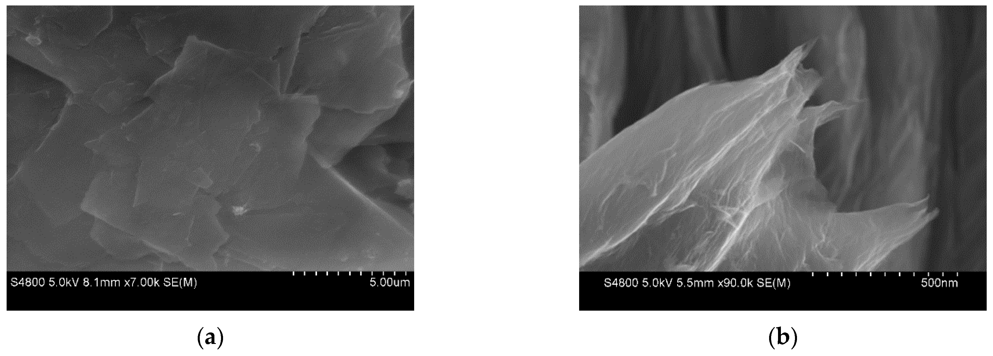

Figure 4.
Raman spectra of graphite micro-flake powders and recovered samples.

Figure 5.
Typical XRD patterns of raw graphite flake and recovered samples.

Figure 6.
Typical XPS spectra of recovered samples. (a) C1s spectrum of Sample No. 1 and (b) C2s spectrum of Sample No. 2.
Figure 6.
Typical XPS spectra of recovered samples. (a) C1s spectrum of Sample No. 1 and (b) C2s spectrum of Sample No. 2.

Figure 7.
Typical FT-IR spectra of Sample No. 1 and Sample No. 2.
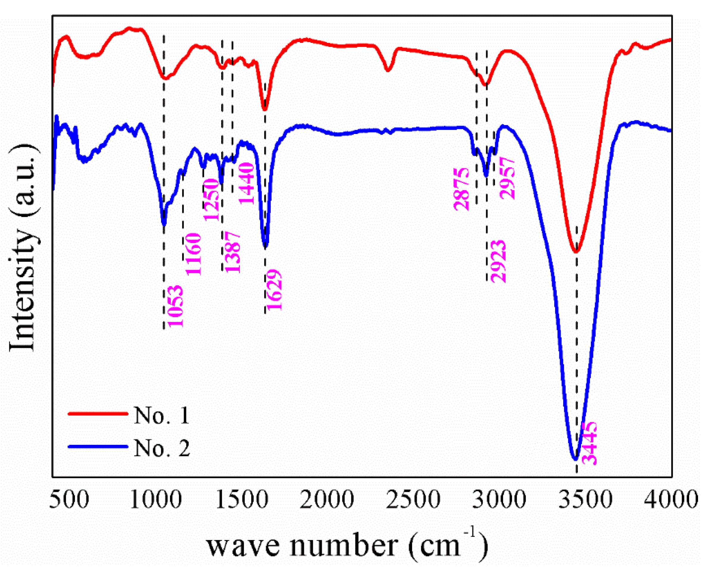
Figure 8.
Typical discharge current and voltage curves of liquid pulsed discharge in micro graphite flake suspension.
Figure 8.
Typical discharge current and voltage curves of liquid pulsed discharge in micro graphite flake suspension.

Figure 9.
Schematic illustration of the formation of few-layer graphene using pulsed discharge in graphite micro-flake suspension.
Figure 9.
Schematic illustration of the formation of few-layer graphene using pulsed discharge in graphite micro-flake suspension.

Table 1.
The experimental conditions of liquid pulsed discharge and characterization results of the recovered samples *.
Table 1.
The experimental conditions of liquid pulsed discharge and characterization results of the recovered samples *.
| No. | Graphite Flake Powder Size | U (kV) | E (J) | Main Carbon Phase | Size of Graphene Nanosheet | Yield | I2D/IG | ID/IG |
|---|---|---|---|---|---|---|---|---|
| 1 | ~10 μm mesh | 30 | 5625 | FLG (3–8 L) | 0.5–10 μm | 23% | 1.35 | 0.25 |
| 2 | ~10 μm mesh | 40 | 10,000 | FLG (4–7 L) | 0.5–10 μm | 30% | 1.44 | 0.40 |
| 3 | ~30 μm mesh | 30 | 5625 | FLG (3–9 L) | 15–25 μm | 21% | 1.32 | 0.30 |
| 4 | ~300 μm mesh | 30 | 5625 | FLG (6–9 L) | ~100 μm | 20% | 1.36 | 0.33 |
* U is the charging voltage, E is the energy stored in capacitor before discharge, FLG is short for few-layer graphene.
© 2019 by the authors. Licensee MDPI, Basel, Switzerland. This article is an open access article distributed under the terms and conditions of the Creative Commons Attribution (CC BY) license (http://creativecommons.org/licenses/by/4.0/).
Share and Cite
MDPI and ACS Style
Gao, X.; Yokota, N.; Oda, H.; Tanaka, S.; Hokamoto, K.; Chen, P.; Xu, M. Preparation of Few-Layer Graphene by Pulsed Discharge in Graphite Micro-Flake Suspension. Crystals 2019, 9, 150. https://doi.org/10.3390/cryst9030150
AMA Style
Gao X, Yokota N, Oda H, Tanaka S, Hokamoto K, Chen P, Xu M. Preparation of Few-Layer Graphene by Pulsed Discharge in Graphite Micro-Flake Suspension. Crystals. 2019; 9(3):150. https://doi.org/10.3390/cryst9030150
Chicago/Turabian StyleGao, Xin, Naoaki Yokota, Hayato Oda, Shigeru Tanaka, Kazuyuki Hokamoto, Pengwan Chen, and Meng Xu. 2019. "Preparation of Few-Layer Graphene by Pulsed Discharge in Graphite Micro-Flake Suspension" Crystals 9, no. 3: 150. https://doi.org/10.3390/cryst9030150
Note that from the first issue of 2016, this journal uses article numbers instead of page numbers. See further details here.