Article

CuZnSn(SxSe1-x)4 Solar Cell Prepared by the Sol-Gel Method Following a Modified Three-Step Selenization Process

1
School of Materials Science and Engineering, Hebei University of Technology, Tianjin 300130, China
2
Science and Technology on Power Sources Laboratory, Tianjin Institute of Power Sources, Tianjin 300130, China
3
Hebei Key Laboratory of Boron Nitride Micro and Nano Materials, Hebei University of Technology, Tianjin 300130, China
4
School of Chemical Engineering, Dalian University of Technology, Dalian 116024, China
5
School of Electrical and Electronic Engineering, Tianjin Key Laboratory of Film Electronic & Communication Devices, Tianjin University of Technology, Tianjin 300191, China
6
School of Physical Science and Technology, Southwest University, Chongqing 400715, China
*
Authors to whom correspondence should be addressed.
Crystals 2019, 9(9), 474; https://doi.org/10.3390/cryst9090474
Submission received: 19 August 2019 / Revised: 3 September 2019 / Accepted: 6 September 2019 / Published: 11 September 2019
(This article belongs to the Special Issue Advances in Thin Film Solar Cells)

Abstract

:
In current work, Cu2ZnSn(S,Se)4 thin films have been prepared by the sol-gel method based on dimethyl sulfoxide solution followed by a modified three-step selenization process. The key process of this method is to divide the Se evaporation and annealing into two different stages: employ a thermal cracking Se source in the Se evaporation stage and an above-atmospheric pressure in the annealing process. The morphological, structural, elemental distributional, and photovoltaic properties of Cu2ZnSn(S,Se)4 thin films prepared with the three-step selenization process were systematically investigated. It was found that through this modified selenization process, the formations of secondary phases (ZnSe, CuSnSe3) and a fine-grain bottom layer, which usually exists in the traditional one-step selenization process, were effectively suppressed. These improvements could further reduce the carrier recombination and improve the solar cell performance. The best solar cell is obtained with a short-circuit current density of 28.16 mA/cm2, open-circuit voltage of 404.91 mV, fill factor of 62.91%, and a power conversion efficiency of 7.17% under air mass 1.5 (100 mW/cm2) illumination.

1. Introduction

Second generation thin film solar cells such as cadmium telluride (CdTe) and copper indium gallium diselenide (CIGS) are currently attracting a lot of attention for their low-capital cost and high efficiency [1,2]. However, concerns about the use of expensive and toxic elements (In and Cd) have led researchers to seek out an alternative material system [3]. Among different candidates, Cu2ZnSn(S,Se)4 (CZTSSe) might be a promising material owing to its abundance, low cost, and environmentally friendly properties [4]. Additionally, CZTSSe has a high optical absorption coefficient (>104 cm−1) and a direct band gap with high tunability by simply changing the S/Se ratio [5].
Up to now, several methods have been proposed to fabricate the CZTSSe solar cells, such as sputtering deposition [6], co-evaporation [7], electrodeposition [8], pulsed laser deposition [9], solution ink printing [10], and the sol-gel method [11,12]. Until now, the highest obtained power conversion efficiency of the CZTSSe solar cell is 12.6% using a type of pure hydrazine-based molecular solution [13]. Conventionally, for the CZTSSe solar cell preparation based on solution methods, a post-selenization is commonly needed. Thus, this process has been investigated extensively [14,15]. For example, Zhao et al. have studied the effect of annealing time and heating rate in ambient Se vapour [16]; Yao et al. prepared CZTSSe solar cells by selenization at a low pressure with Se and SnSe2 sources [17]; Xin et al. adopted the absorber selenization process under high argon pressure [18]. Moreover, the selenization process usually results in the formation of a bi-layer structure with bi-modal grain size, which consists of a rough-grain upper layer and a fine-grain bottom layer [11,16,19]. The fine-grain underlayer contains various residual organic solvent and secondary phases (ZnSe, ZnS, SnSe2, SnS, Cu2Se, Cu2S, CuSnSe3 et al.), which could greatly impact the performance of CZTSSe solar cells [20]. In general, the formation of the bi-layer structure is due to that, in the annealing process, the Se vapour can not fully reach the bottom of the CZTS precursor layer, which is caused by the restrained further diffusion of Se atoms from the crystallized grain in the upper layer. In order to effectively reduce this bi-layer structure and improve the crystal quality, Jong-Ok Jeon applied the thermal annealing process at high Se pressure and successfully reduced the thickness of the fine-grain underlayer [21]. However, selenization at high Se pressure is highly likely to introduce a thick MoSe2 layer formation, which in turn degrades the performance of the solar cell device [22]. Therefore, an effective selenization process is urgently needed to further optimize the preparation of CZTSSe solar cells based on the solution method and enhance their performance.
In this study, we designed and proposed a new three-step selenization process with respect to the conventional one-step process. In our selenization process, we divided the Se evaporation and annealing into two different stages to obtain a large grain layer without other secondary phases. In the Se evaporation stage, a thermal cracking Se source was used to disperse the Se atoms among the precursor film. Then, in the annealing stage, an above-atmospheric pressure was adopted to reduce the loss of Sn and enhance Se diffusion. The structural morphology, elemental distribution, and photovoltaic properties of the prepared CZTSSe thin film with the three-step selenization process were systematically studied. As we anticipated, a better crystal quality was obtained with effective suppression of other second phases. In the end, CZTSSe solar cells prepared with our proposed method showed much better performance with greatly improved efficiency of 7.17% under air mass 1.5 (100 mW/cm2) illumination.

2. Experimental Details

The precursor solution was prepared by successively dissolving 10 mmol Cu(CH3COO)2 and 6.7 mmol SnCl2 in 80 mL dimethyl sulfoxide (DMSO) solution with stirring overnight. Then, 7 mmol ZnCl2 and 38.8 mmol thiourea were added and it was further stirred for another two hours to obtain a clear yellow solution. All chemicals were 99% purity and purchased from Aladdin (Shanghai, China).
The CZTS precursor films were spin-coated onto the molybdenum coated soda-lime glass substrates at a speed of 1540 rpm for 50 s and were then immediately annealed on a 540 °C hotplate for 5 min. This process was repeated seven times. All the processes were carried out in an argon filled glovebox system with oxygen and water less than 10 ppm, including all the solution preparation, thin film spin-coating, and annealing.
In order to complete the preparation of the CZTSSe film, a three-step selenization process was carried out. In the first step, the precursor film was put into a vacuum chamber under 10−3 Pa background pressure. Without argon flow, the sample without substrate heating (<70 °C) was annealed for 5 min under an 800 °C thermal cracking Se source. In this step, the Se atoms could diffuse into the CZTS precursor and did not react with CZTS particles. For the second step, the annealed CZTS precursor film was put into a graphite box (Bohua Tec, Tianjin, China) with 50 mg Se pellets and selenized at 530 °C for 10 min in a furnace under an above-atmospheric pressure (1.2 × 10⁵ Pa) without argon flow. During the third step, the furnace was kept at 320 °C for another 10 min to eliminate the residual Se on the surface of the film and was naturally cooled down to room temperature. For comparison, one control sample was prepared by the widely applied one-step selenization process [23], and the temperature and annealing time were optimized according to our previous work. The specific process was that the CZTS precursor film was put in a graphite box with 200 mg Se pellets and selenized at 530 °C for 20 min in a furnace under argon gas flow and was then cooled down to room temperature naturally.
After the selenization process, a 60 nm CdS layer was deposited on the CZTSSe film by chemical bath deposition (CBD). Then, by the RF sputtering method, a 50 nm i-ZnO layer and 350 nm Al-doped ZnO layer were deposited sequentially. Finally, the solar cell fabrication was finished by e-beam evaporation of Ni–Al top electrode using a shadow mask. Each sample of 4 × 4 cm2 contained 12 sub solar cells and each one was 0.38 cm2.
The morphological properties of the thin films were examined with a Hitachi S4800 field emission scanning electron microscope (FE-SEM) (HITACHI, Tokyo, Japan). X-ray diffraction (XRD) (Rigaku, Tokyo, Japan) patterns were measured with a M18XHF-SRA diffractometer (Rigaku, Tokyo, Japan) with monochromatic Cu Kα radiation. Raman spectrum (Renishaw, London, UK) was analyzed with a Nd-YAG 532 nm laser in a Horiba Jobin Yvon T64000 spectroscopy (Renishaw, London, UK). The elemental composition measurements were carried out with Thermal i-cap 6300 inductively coupled plasma mass spectrometry (ICP) (Thermal, San Francisco, USA). The depth profiles of the elements were obtained by secondary ion mass spectroscopy (SIMS, IMS-4F) (Cameca, Paris, France). Current-voltage (J-V) measurements were performed using a Keithley 2400 source-measure unit under 100 mW/cm2 simulated AM1.5G illumination from a xenon arc lamp with a AM1.5G filter (Daheng Tec, Beijing, China).

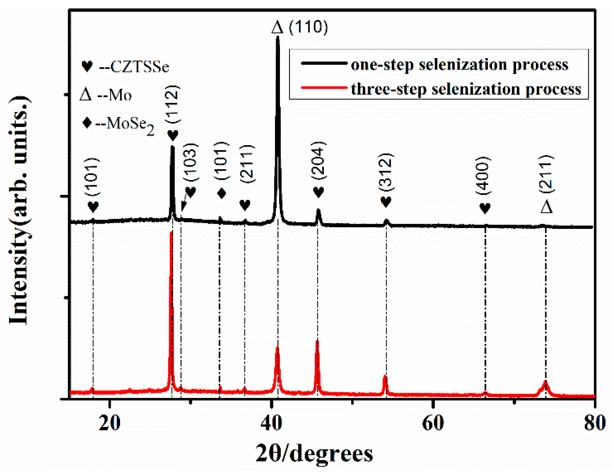
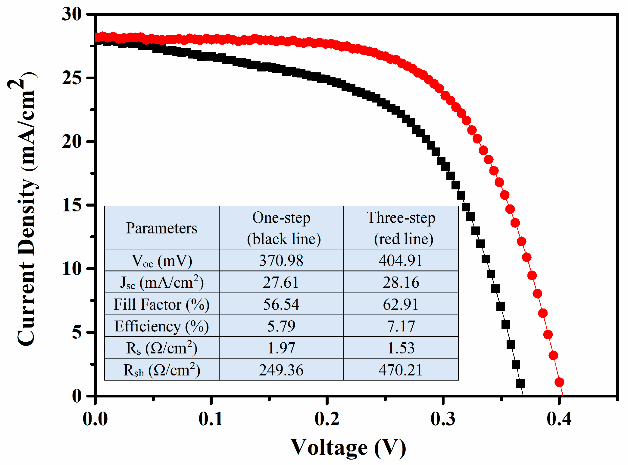
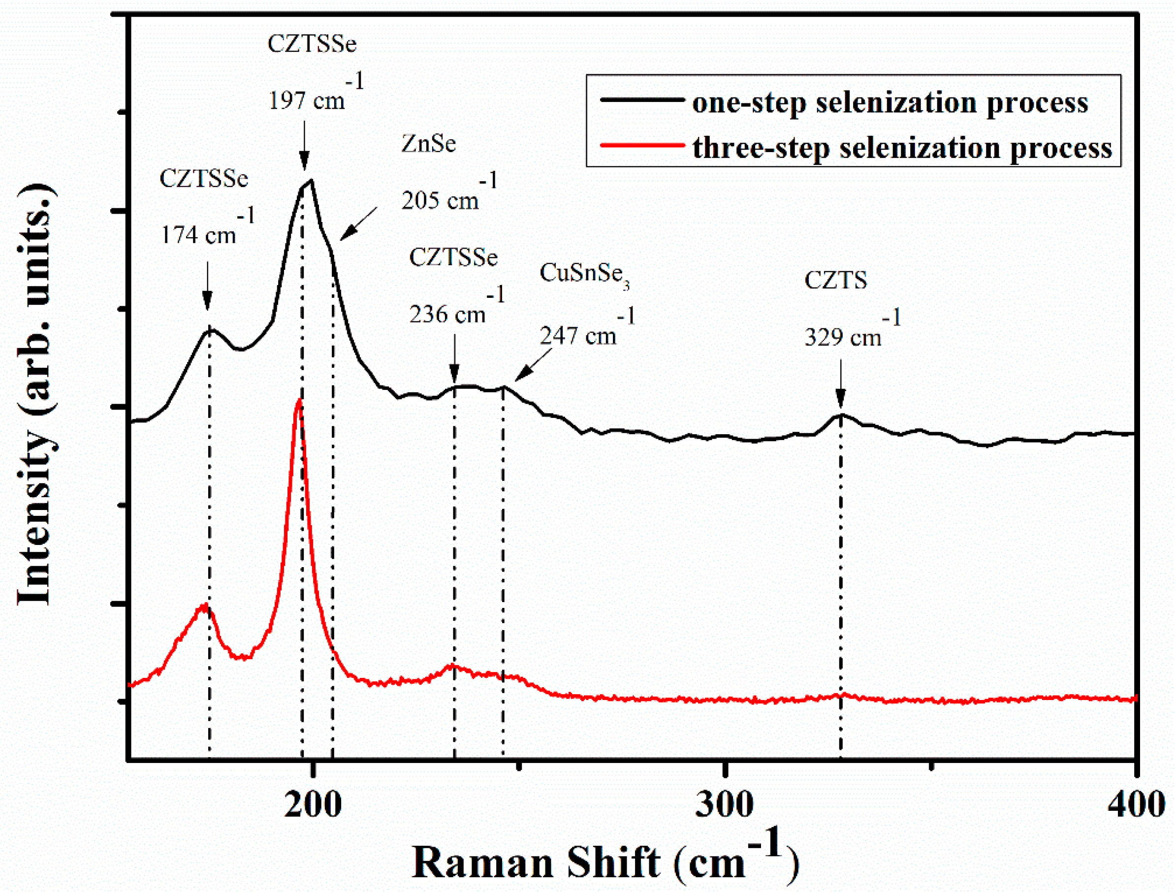
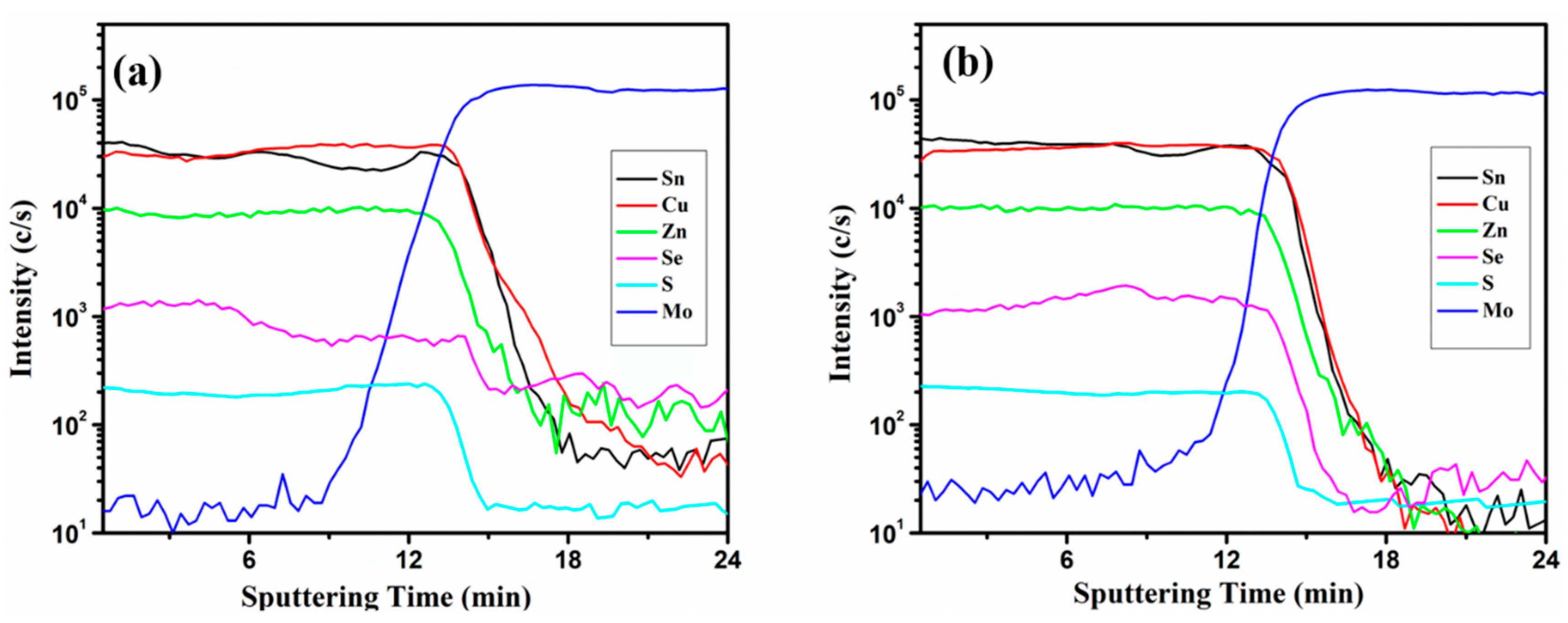
3. Results and Discussions

The elemental compositions of the CZTS precursor film and selenized CZTSSe films prepared with both the conventional one-step and our modified three-step process are listed in Table 1. By comparing the CZTSSe films fabricated by the one-step and three-step selenization process, the sample with the three-step selenization process shows both a lower Zn/Sn and Cu/(Zn + Sn) ratio. Besides, it is also found that the CZTSSe film with the three-step selenization process has a higher residual S content. Based on previous works [8,24,25], the loss of Sn element is mainly caused by the evaporation of SnS and SnSe phases and the formation of various defects and composition segregation. This phenomenon could hamper the performance of CZTSSe solar cells [25]. Herein, our result of S content increase in the sample prepared with the three-step process indicates that this modified three-step selenization process could effectively suppress the loss of Sn and S elements and secondary phase formation.
Figure 1 shows the FE-SEM images of the CZTS precursor and CZTSSe thin films. Figure 1(a–f) correspond the top surface and cross-sectional images of the CZTS precursor and the CZTSSe films with the one-step and three-step selenization process, respectively. As shown in Figure 1(a), there are numerous holes and cracks in the surface of the CZTS precursor film, and these defects provide the channel for the diffusion of Se atoms. By comparing the images of CZTSSe films with the one-step and three-step selenization process, we can observe that the crystallinity of CZTSSe films with the three-step selenization process is enhanced with a larger grain size. Further, both of the two samples show a bi-layer structure. As explained before, the formation of the bi-layer structure is due to the Se vapour reacting with the upper CZTS particles and translating to a CZTSSe crystallized grain layer. Further, the upper CZTSSe layer might restrain the further diffusion of Se atoms to the CZTS underlayer. The absence of Se causes numerous second phase formations. A closer look shows that the film with the one-step selenization process shows a fine-grain bottom layer. Whereas, the film with the three-step selenization process does not have a fine-grain layer; both the bottom and top layers show a large grain structure. This fine-grain layer usually contains a lot of secondary phases, such as ZnS(e) and SnS(e), which could hinder the carrier transportation. This different bottom layer morphology from the three-step process is owing to the fact that Se atoms can diffuse through the CZTS precursor film more homogeneously without the substrate heating in the first step.
Figure 2 shows the XRD patterns of CZTSSe thin films prepared with both the one-step and three-step selenization process. Both the samples have several prominent reflections along the (112), (211), (204), and (312) planes, which verifies the formation of the CZTSSe structures [PDF#97-009-5117]. In comparison, the (112) peak of the CZTSSe thin films with the three-step selenization process exhibits a much higher intensity than the sample with the one-step selenization process. The size of the crystallites was precisely calculated by the Scherrer equation according to the location and full width at half maximum (FWHM) of the main diffraction (112) peak [26]:
D = k λ β c o s θ
where D is the size of the regions of coherent scattering; k (=0.89) is the shape factor; β is the width of the diffraction peak at its half maximum; and λ is the wavelength of the used radiation (=0.15406 nm). The obtained D values calculated by equation (1) are 212.6 nm and 343.2 nm for the CZTSSe film prepared by the one-step and three-step process, respectively. These results indicate that the crystallinity of CZTSSe film was greatly enhanced with the three-step selenization process. In the three-step selenization process, adopting an above atmospheric pressure (1.2 × 10⁵ Pa) may suppress the evaporation of Se element, and a high liquid Se content may promote CZTSSe grain growth. Another apparent diffraction peak in the XRD patterns is the (101) of MoSe2 (marked by ♦). We observe that both the two samples fabricated by the one-step and three-step selenization process have a similar MoSe2 (101) peak intensity. Further, from the SEM images, we observed that the thicknesses of the MoSe2 layers are less than 100 nm. The similar, thin MoSe2 layer would not affect the performance of CZTSSe solar cells.
Owing to the existence of some binary (cubic ZnS, ZnSe) and ternary (tetragonal Cu2SnSe3) chalcogenides, the XRD pattern is not sufficient to determine the phase purity of the synthesized materials. Thus, we also used Raman spectrum to characterize their structures. As seen in Figure 3, we find that ZnSe and CuSnSe3 phases exist in the CZTSSe film with the one-step selenization process. However, these secondary phases disappear in the CZTSSe film with the three-step selenization process. The Raman results indicate that the three-step selenization process could eliminate the fine bottom layer of the CZTSSe film which contained a lot of the secondary phase (ZnSe, CuSnSe3), as also observed with the microscopic morphology in Figure 1.
To assess the element distribution along the film thickness direction, secondary ion mass spectroscopy (SIMS) analysis was carried out. From Figure 4, we can see that the CZTSSe film with the three-step selenization process shows a uniform distribution of Se element throughout the film. The Se contents are higher in the top layer than in the bottom layer and the S is distributed mostly homogeneously among the film. This indicates that the three-step selenization process could be beneficial for Se element diffusion.
In the end, the CZTSSe solar cells were prepared and the current density-voltage (J-V) curves were measured and are shown in Figure 5. The CZTSSe solar cells with the one-step selenization process exhibited an efficiency of 5.79% with an open-circuit voltage (Voc) of 370.98 mV, a short-circuit current density (Jsc) of 27.61 mA/cm2, a fill factor of 56.54%. Then, the efficiency of CZTSSe solar cells with the three-step selenization process increase to 7.17% with Voc of 404.91 mV, Jsc of 28.16 mA/cm2, and a fill factor of 62.91%. Remarkably, with the three-step selenization process, the series resistance (Rs) decreases from 1.97 Ω/□ to 1.53 Ω/□, and the shunt resistance (Rsh) increases from 249.36 Ω/□ to 470.21 Ω/□. The series resistance decrease is induced by the fine-grain bottom layer elimination, which has numerous secondary phases. Then, the shunt resistance increase is mainly caused by grain growth, which could reduce the channels of carrier recombination in the CZTSSe thin films. Another important point that should be noted is that the Voc value is nearly elevated to 34 mV.
To make the effect of the three-step selenization process on the band gap of CZTSSe solar cells clear, the external quantum efficiency (EQE) measurement was carried out and the results are shown in Figure 6. The EQE spectrum at short wavelengths (below 520 nm) indicates that the two CZTSSe solar cells with different selenization processes exhibit similar absorption originating from the CdS/i-ZnO/AZO top layers. Further, comparable, incomplete absorptions of the absorber occur close to respective bandgaps, which is likely attributed to the insufficient thickness of the CZTSSe absorbed layer. The Jsc values measured by the EQE are 27.68 mA/cm2 and 28.10 mA/cm2 for the CZTSSe solar cell with the one-step and three-step selenization process and these results are in agreement with the J-V curves. Then, the bandgap of the absorber can be derived from the data near the band edge by plotting [E×ln(1-EQE)]2 versus E [27], as plotted in the inset figure. From the fitting results, it is found that the difference value of the band gap between the two selenization processes is merely 0.007 eV. Another important point that should be noted is that a gap exists between 845 nm to 1030 nm, which was caused by the difference of carrier’s collection [28]. So, based on the EQE measurement, the three-step selenization process does not improve the absorber band gap. The improvements of both Voc and Jsc are due to the decrease of the carrier recombination defects existing mainly in the grain and boundary.

4. Conclusions

In summary, we have demonstrated that the CZTSSe thick films were fabricated with the sol-gel method followed by a modified three-step selenization process. Compared to the traditional one-step selenization process, we divided the Se evaporation and annealing into two different stages, and through adopting the above-atmospheric pressure, the formation of a homogeneous large grain layer was promoted with the secondary phases (ZnSe, CuSnSe3) effectively restrained. All these improvements could reduce the carrier recombination and then enhance the performance of CZTSSe solar cells with the efficiency increased from 5.79% to 7.17%.

Author Contributions

Conceptualization, X.S. and G.L.; methodology, C.Z. and T.Y.; software, Y.Z.; validation, C.T.; formal analysis, X.S. and C.T.; investigation, X.S. and T.Y.; resources, W.L. and G.C.; data curation, X.S.; writing—original draft preparation, X.S. and C.Z.; writing—review and editing, C.T. and T.Y.; visualization, G.C.; supervision, C.T. and T.Y.; project administration, X.S.; funding acquisition, W.L. and G.C.

Funding

This research was funded by the National Natural Science Foundation of China, grant number 61804108, 61674051, and 51871089.

Acknowledgments

The authors thank the anonymous reviewers for their constructive suggestions.

Conflicts of Interest

The authors declare no conflict of interest.

References

  1. Burst, J.M.; Duenow, J.N.; Albin, D.S.; Colegrove, E.; Reese, M.O.; Aguiar, J.A.; Jiang, C.S.; Patel, M.K.; Al-Jassim, M.M.; Kuciauskas, D.; et al. CdTe solar cells with open-circuit voltage breaking the 1 V barrier. Nat. Energy 2016, 1, 16015. [Google Scholar] [CrossRef]
  2. Reinhard, P.; Buecheler, S.; Tiwari, A.N. Technological status of Cu(In,Ga)(Se,S)2-based photovoltaics. Sol. Energy Mater. Sol. Cells 2013, 119, 287–290. [Google Scholar] [CrossRef]
  3. Wadia, C.; Alivisatos, A.P.; Kammen, D.M. Materials availability expands the opportunity for large-scale photovoltaics deployment. Environ. Sci. Technol. 2009, 43, 2072–2077. [Google Scholar] [CrossRef] [PubMed]
  4. Zhao, W.; Wang, G.; Tian, Q.; Huang, L.; Gao, S.; Pan, D. Solution-processed Cu2CdSn(S,Se)4 thin film solar cells. Sol. Energy Mater. Sol. Cells 2015, 133, 15–20. [Google Scholar] [CrossRef]
  5. Pal, K.; Singh, P.; Bhaduri, A.; Thapa, K.B. Current challenges and future prospects for a highly efficient (>20%) kesterite CZTS solar cell: A review. Sol. Energy Mater. Sol. Cells 2019, 196, 138–156. [Google Scholar] [CrossRef]
  6. Li, J.; Wang, H.; Luo, M.; Tang, J.; Chen, C.; Liu, W.; Liu, F.; Sun, Y.; Han, J.; Zhang, Y. 10% Efficiency Cu2ZnSn(S,Se)4 thin film solar cells fabricated by magnetron sputtering with enlarged depletion region width. Sol. Energy Mater. Sol. Cells 2016, 149, 242–249. [Google Scholar] [CrossRef]
  7. Lee, Y.S.; Gershon, T.; Gunawan, O.; Todorov, T.K.; Gokmen, T.; Virgus, Y.; Guha, S. Cu2ZnSnSe4 Thin-Film Solar Cells by Thermal Co-evaporation with 11.6% Efficiency and Improved Minority Carrier Diffusion Length. Adv. Energy Mater. 2015, 5, 1401372. [Google Scholar] [CrossRef]
  8. Yao, L.; Ao, J.; Jeng, M.-J.; Bi, J.; Gao, S.; Sun, G.; He, Q.; Zhou, Z.; Zhang, Y.; Sun, Y.; et al. Reactive Mechanism of Cu2ZnSnSe4 Thin Films Prepared by Reactive Annealing of the Cu/Zn Metal Layer in a SnSex + Se Atmosphere. Crystals 2018, 9, 10. [Google Scholar] [CrossRef]
  9. Moholkar, A.V.; Shinde, S.S.; Babar, A.R.; Sim, K.-U.; Lee, H.K.; Rajpure, K.Y.; Patil, P.S.; Bhosale, C.H.; Kim, J.H. Synthesis and characterization of Cu2ZnSnS4 thin films grown by PLD: solar cells. J. Alloy. Compd. 2011, 509, 7439–7446. [Google Scholar] [CrossRef]
  10. Lin, X.; Klenk, R.; Wang, L.; Köhler, T.; Albert, J.; Fiechter, S.; Ennaoui, A.; Lux-Steiner, M.C. 11.3% efficiency Cu(In,Ga)(S,Se)2 thin film solar cells via drop-on-demand inkjet printing. Energy Environ. Sci. 2016, 9, 2037–2043. [Google Scholar] [CrossRef]
  11. Xin, H.; Katahara, J.K.; Braly, I.L.; Hillhouse, H.W. 8% Efficient Cu2ZnSn(S,Se)4 Solar Cells from Redox Equilibrated Simple Precursors in DMSO. Adv. Energy Mater. 2014, 4, 1301823. [Google Scholar] [CrossRef]
  12. Haass, S.G.; Diethelm, M.; Werner, M.; Bissig, B.; Romanyuk, Y.E.; Tiwari, A.N. 11.2% Efficient Solution Processed Kesterite Solar Cell with a Low Voltage Deficit. Adv. Energy Mater. 2015, 5, 1500712. [Google Scholar] [CrossRef]
  13. Wang, W.; Winkler, M.T.; Gunawan, O.; Gokmen, T.; Todorov, T.K.; Zhu, Y.; Mitzi, D.B. Device Characteristics of CZTSSe Thin-Film Solar Cells with 12.6% Efficiency. Adv. Energy Mater. 2014, 4, 1301465. [Google Scholar] [CrossRef]
  14. Schnabel, T.; Abzieher, T.; Friedlmeier, T.M.; Ahlswede, E. Solution-Based Preparation of Cu2ZnSn(S,Se)4 for Solar Cells-Comparison of SnSe2 and Elemental Se as Chalcogen Source. IEEE J. Photovolt. 2015, 5, 670–675. [Google Scholar] [CrossRef]
  15. Stanchik, A.V.; Gremenok, V.F.; Juskenas, R.; Tyukhov, I.I.; Tivanov, M.S.; Fettkenhauer, C.; Shvartsman, V.V.; Giraitis, R.; Hagemann, U.; Lupascu, D.C. Effects of selenization time and temperature on the growth of Cu2ZnSnSe4 thin films on a metal substrate for flexible solar cells. Sol. Energy 2019, 178, 142–149. [Google Scholar] [CrossRef]
  16. Zhao, Y.; Han, X.; Chang, L.; Dong, C.; Li, J.; Yan, X. Effects of selenization conditions on microstructure evolution in solution processed Cu2ZnSn(S,Se)4 solar cells. Sol. Energy Mater. Sol. Cells 2019, 195, 274–279. [Google Scholar] [CrossRef]
  17. Yao, L.; Ao, J.; Jeng, M.J.; Bi, J.; Gao, S.; He, Q.; Zhou, Z.; Sun, G.; Sun, Y.; Chang, L.B.; et al. CZTSe solar cells prepared by electrodeposition of Cu-Sn-Zn stack layer followed by selenization at low Se pressure. Nanoscale Res. Lett. 2014, 9, 678. [Google Scholar] [CrossRef] [PubMed]
  18. Jiang, J.; Yu, S.; Gong, Y.; Yan, W.; Zhang, R.; Liu, S.; Huang, W.; Xin, H. 10.3% Efficient CuIn(S,Se)2 Solar Cells from DMF Molecular Solution with the Absorber Selenized under High Argon Pressure. Sol. RRL 2018, 2, 1800044. [Google Scholar] [CrossRef]
  19. Clark, J.A.; Uhl, A.R.; Martin, T.R.; Hillhouse, H.W. Evolution of Morphology and Composition during Annealing and Selenization in Solution-Processed Cu2ZnSn(S,Se)4. Chem. Mater. 2017, 29, 9328–9339. [Google Scholar] [CrossRef]
  20. Scragg, J.J.; Watjen, J.T.; Edoff, M.; Ericson, T.; Kubart, T.; Platzer-Bjorkman, C. A detrimental reaction at the molybdenum back contact in Cu2ZnSn(S,Se)4 thin-film solar cells. J. Am. Chem. Soc. 2012, 134, 19330–19333. [Google Scholar] [CrossRef]
  21. Jeon, J.O.; Lee, K.D.; Seul Oh, L.; Seo, S.W.; Lee, D.K.; Kim, H.; Jeong, J.H.; Ko, M.J.; Kim, B.; Son, H.J.; et al. Highly efficient copper-zinc-tin-selenide (CZTSe) solar cells by electrodeposition. ChemSusChem 2014, 7, 1073–1077. [Google Scholar] [CrossRef] [PubMed]
  22. Shin, B.; Bojarczuk, N.A.; Guha, S. On the kinetics of MoSe2 interfacial layer formation in chalcogen-based thin film solar cells with a molybdenum back contact. Appl. Phys. Lett. 2013, 102, 091907. [Google Scholar] [CrossRef]
  23. Bucherl, C.N.; Oleson, K.R.; Hillhouse, H.W. Thin film solar cells from sintered nanocrystals. Curr. Opin. Chem. Eng. 2013, 2, 168–177. [Google Scholar] [CrossRef]
  24. Weber, A.; Mainz, R.; Schock, H.W. On the Sn loss from thin films of the material system Cu–Zn–Sn–S in high vacuum. J. Appl. Phys. 2010, 107, 013516. [Google Scholar] [CrossRef]
  25. Bree, G.; Coughlan, C.; Geaney, H.; Ryan, K.M. Investigation into the Selenization Mechanisms of Wurtzite CZTS Nanorods. ACS Appl. Mater. Interfaces 2018, 10, 7117–7125. [Google Scholar] [CrossRef] [PubMed]
  26. Holzwarth, U.; Gibson, N. The Scherrer equation versus the ‘Debye-Scherrer equation’. Nat. Nanotechnol. 2011, 6, 534. [Google Scholar] [CrossRef] [PubMed]
  27. Gokmen, T.; Gunawan, O.; Todorov, T.K.; Mitzi, D.B. Band tailing and efficiency limitation in kesterite solar cells. Appl. Phys. Lett. 2013, 103, 103506. [Google Scholar] [CrossRef]
  28. Temgoua, S.; Bodeux, R.; Naghavi, N. Influence of the annealing atmosphere and precursor’s thickness on the properties of CZTSSe based solar cells. Sol. Energy Mater. Sol. Cells 2019, 191, 123–132. [Google Scholar] [CrossRef]
Figure 1. Surface and cross-sectional SEM images of (a,d) CZTS precursor film, (b,e) CZTSSe film with the one-step selenization process, (c,f) CZTSSe film with the three-step selenization process.
Crystals 09 00474 g001
Figure 2. XRD patterns of CZTSSe film with the one-step and three-step selenization process.
Crystals 09 00474 g002
Figure 3. Raman spectrums of CZTSSe film with the one-step and three-step selenization process.
Crystals 09 00474 g003
Figure 4. Secondary ion mass spectroscopy (SIMS) profiles of CZTSSe films prepared by (a) one-step and (b) three-step selenization process.
Crystals 09 00474 g004
Figure 5. J-V characteristics of the CZTSSe solar cells prepared by the one-step and three-step selenization process.
Crystals 09 00474 g005
Figure 6. External quantum efficiency of CZTS solar cells fabricated by the one-step and three-step selenization process. Inset: Extrapolation of the band gaps from the external quantum efficiency (EQE) data.
Crystals 09 00474 g006
Table 1. The measured chemical compositions of the CZTS precursor film and CZTSSe films.
SampleElement Compositions (%)Composition Ratios
CuZnSnSSeCu/(Zn + Sn)Zn/Sn
Precursor film23.8115.5514.8645.78-0.781.05
Selenide filmsOne-step20.9413.9211.715.1348.310.821.19
Three-step21.0713.9712.035.7947.150.811.16

