

Novel SMD Component and Module Interconnection and Encapsulation Technique for Textile Substrates Using 3D Printed Polymer Materials


Abstract
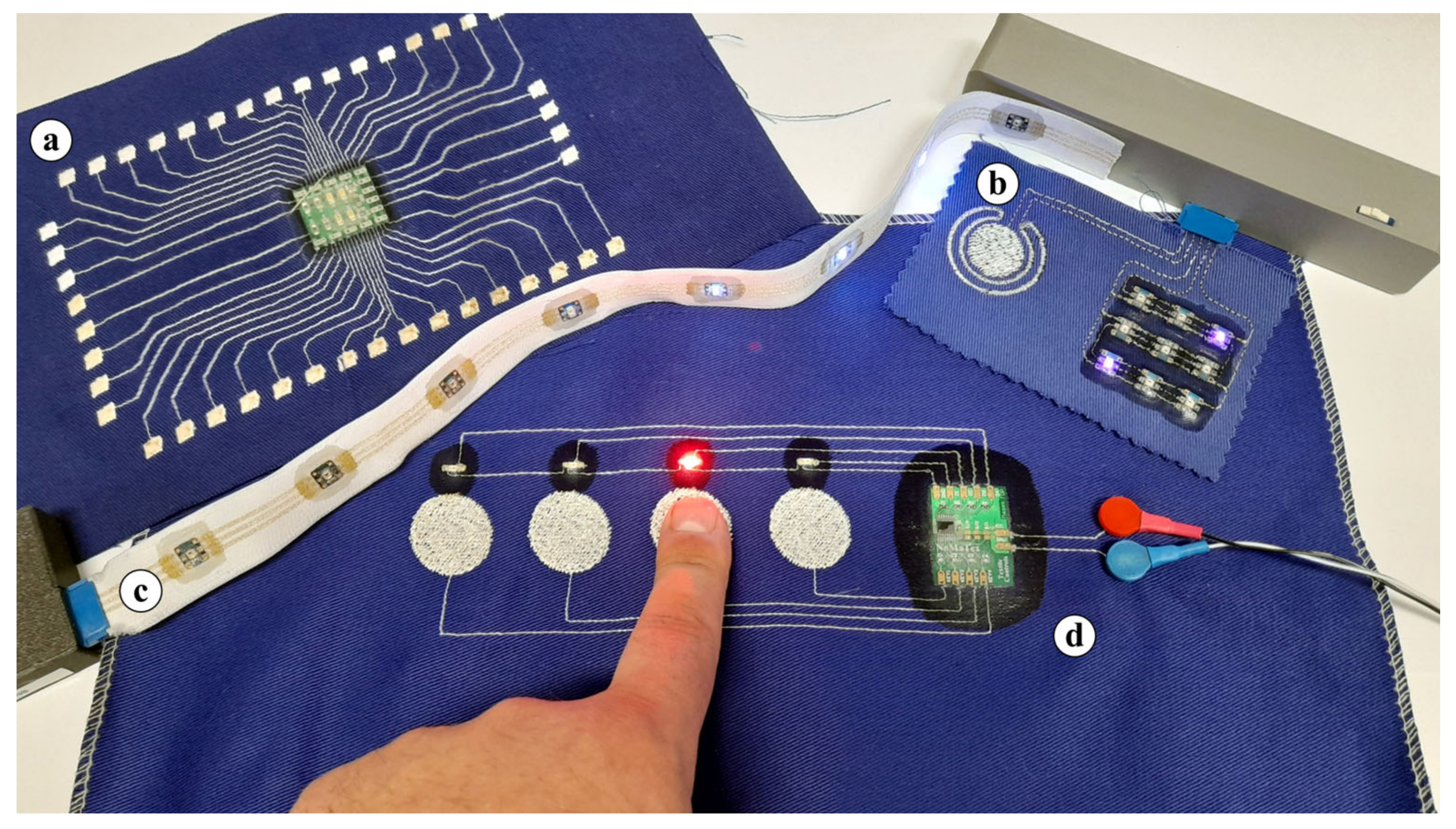
:1. Introduction
2. Materials and Methods
2.1. Thermo-Compression Interconnection Technique
2.2. Design of Electrical Layout
2.3. Design of Component Housing
2.4. 3D Printed Thermoplastic Housing
2.5. Textile Substrate and Conductive Yarn
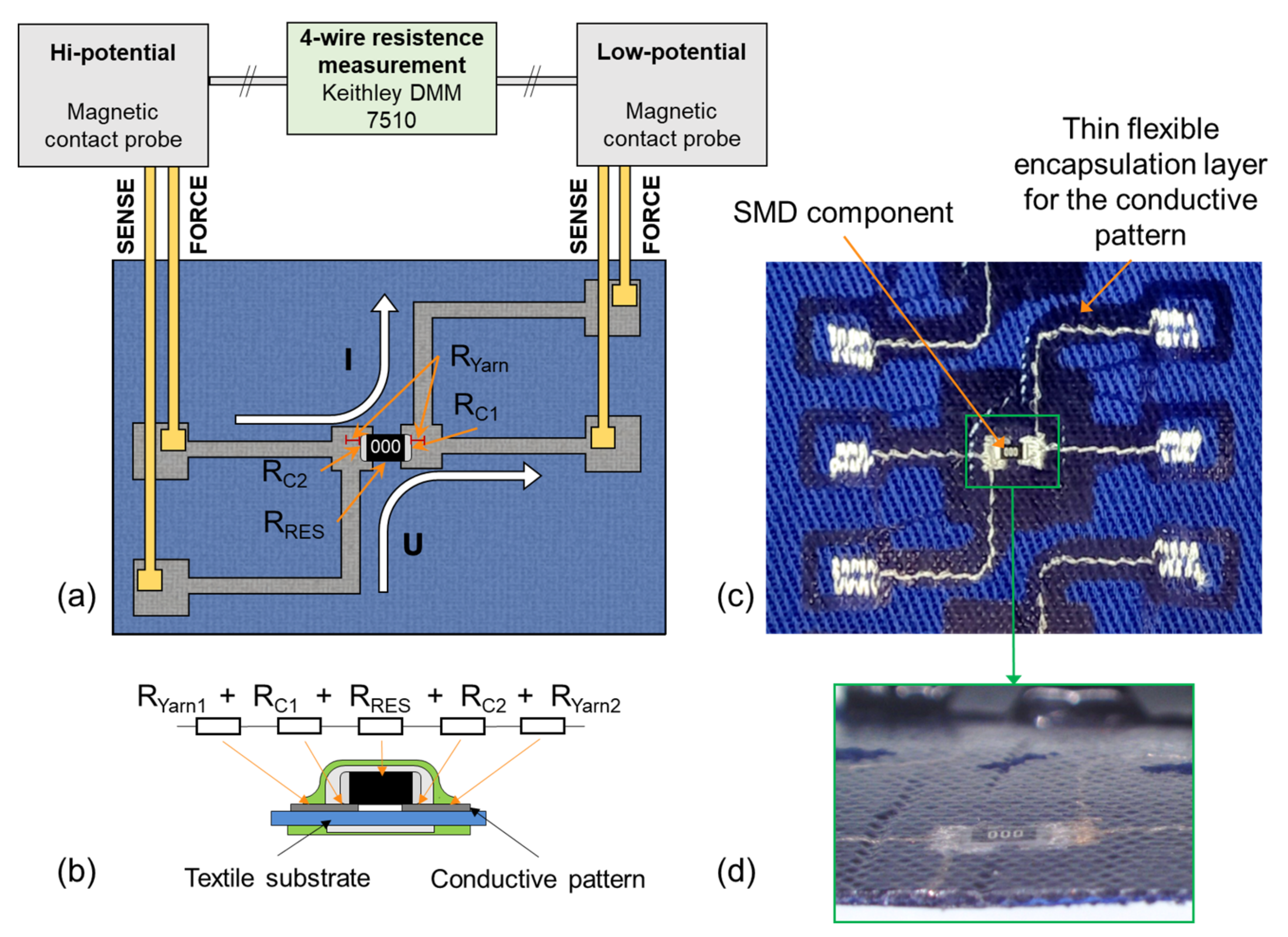
2.6. Electrical Characterization of Contact Resistance
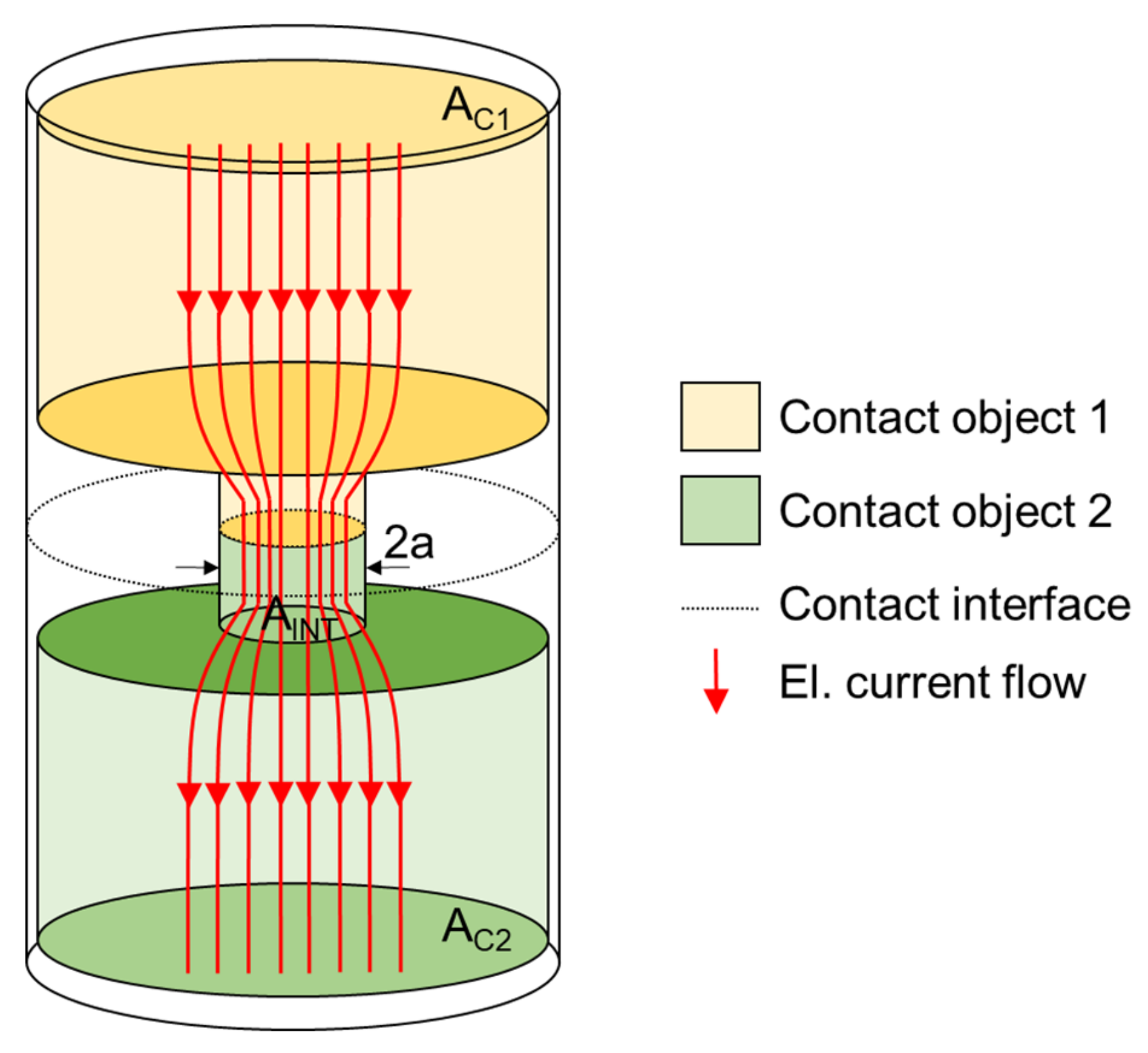
2.7. Theoretical Model of Contact Resistance
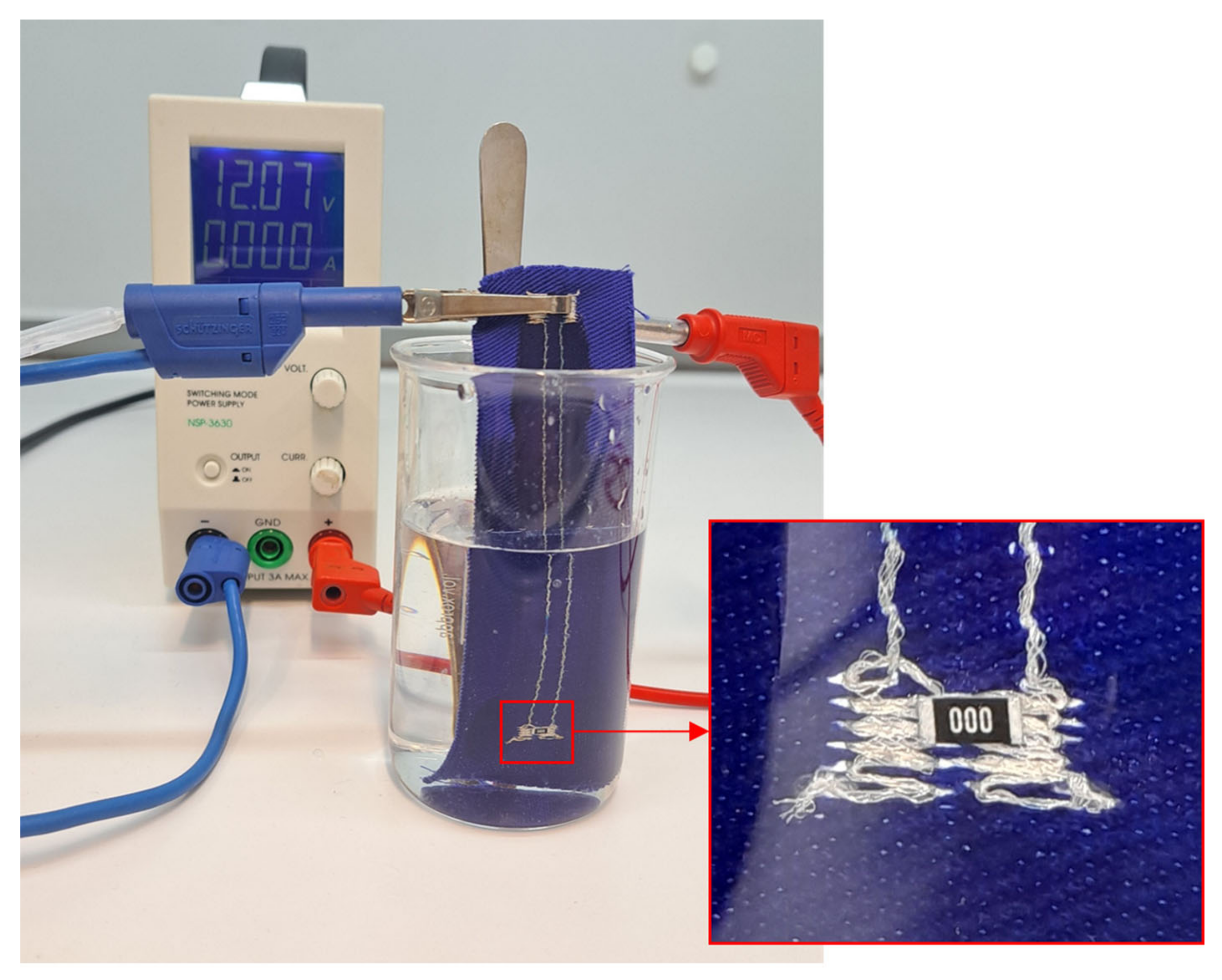
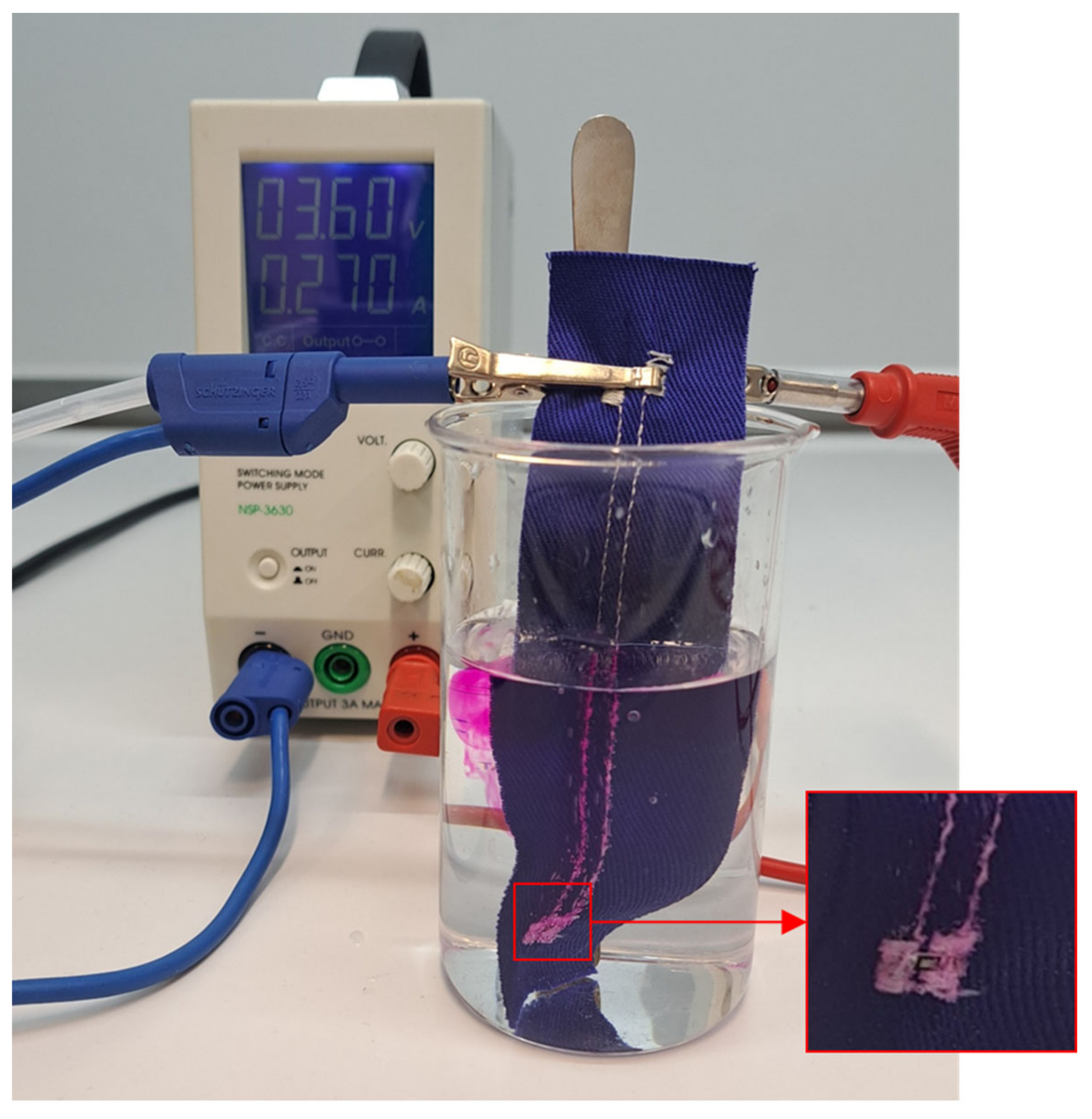
2.8. Quality of Encapsulation
3. Results and Discussion
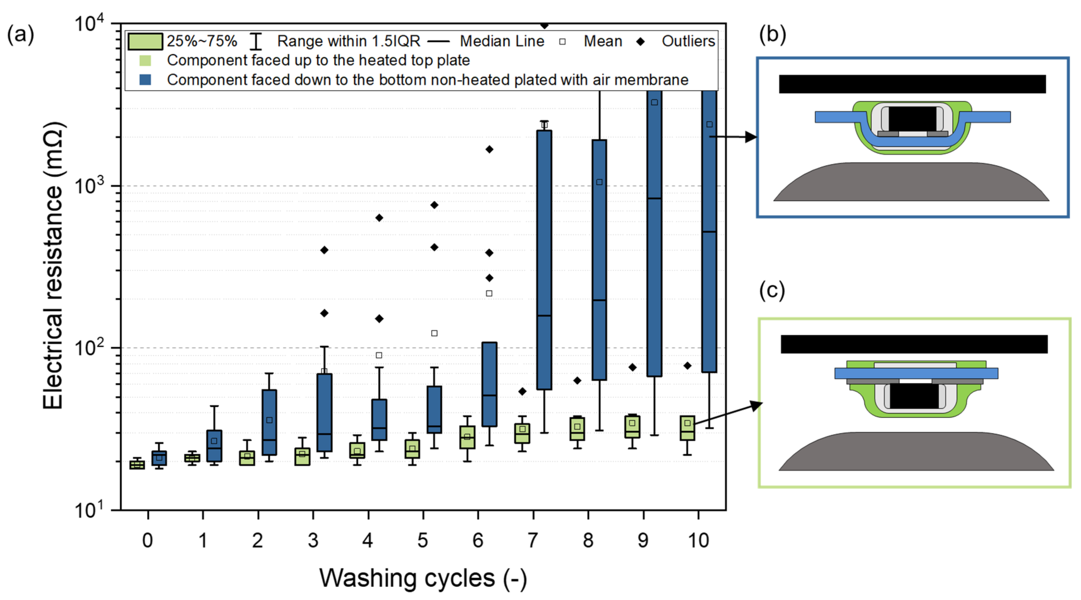
3.1. Component Orientation in the Heat-Press Machine
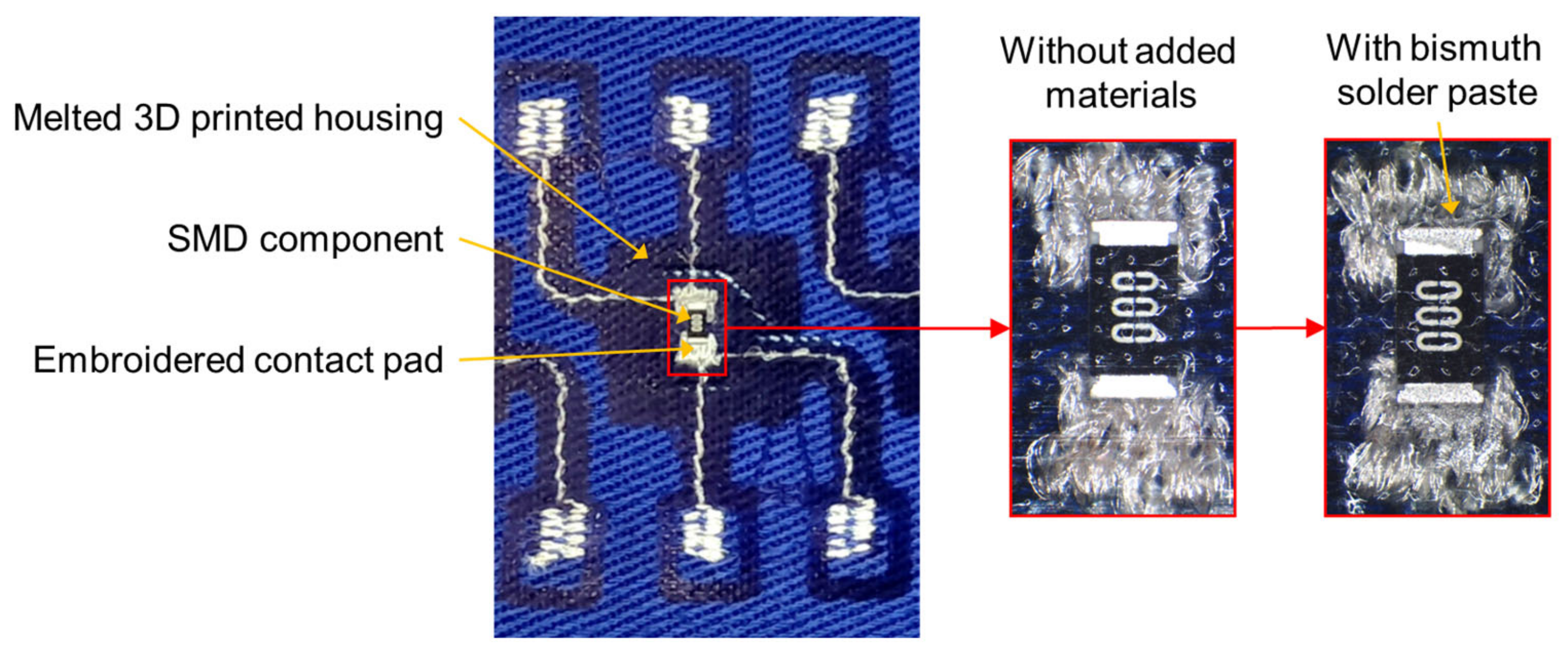
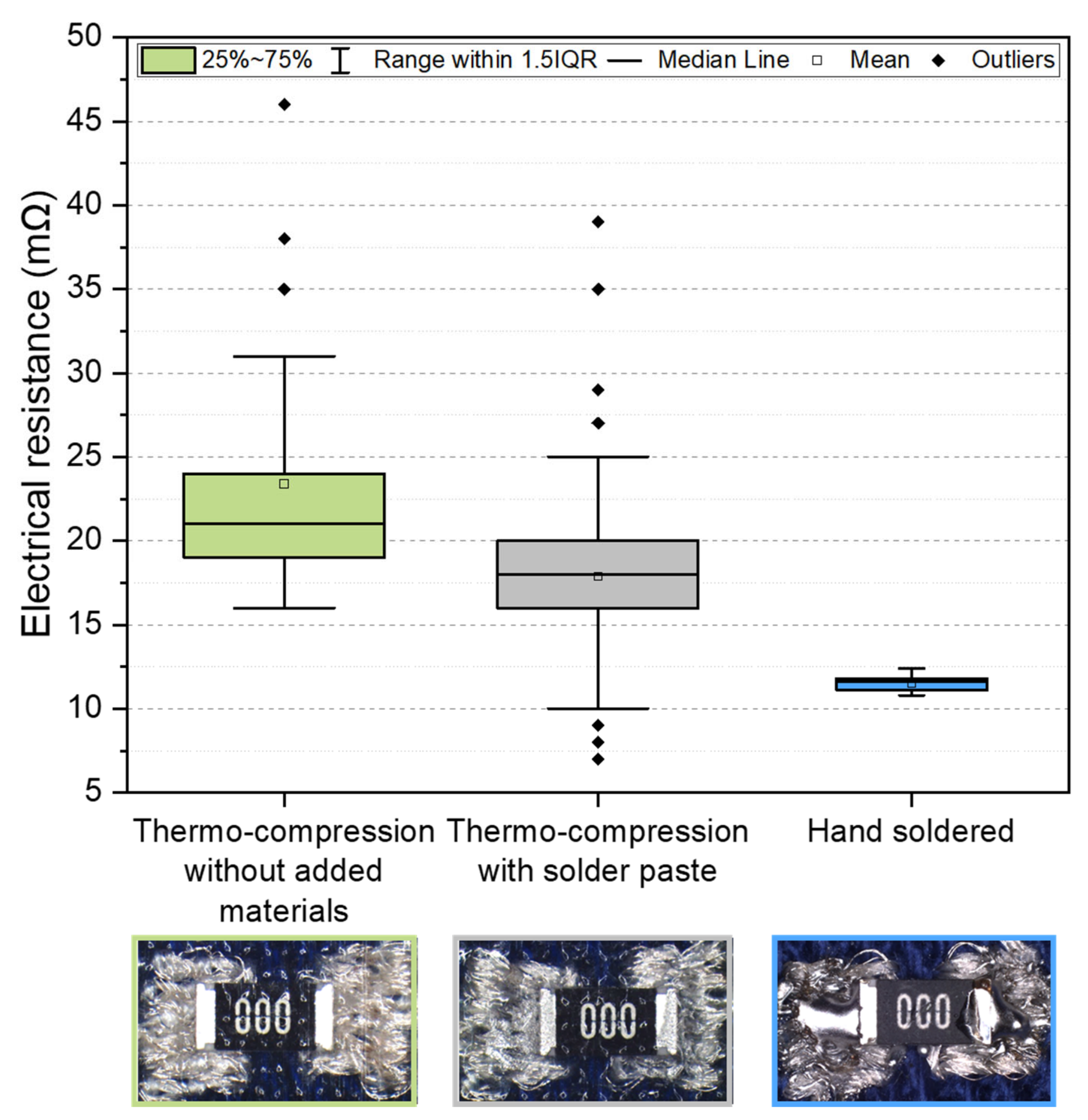
3.2. Specimens with Added Solder Materials for Electrical Conductivity Enhancement
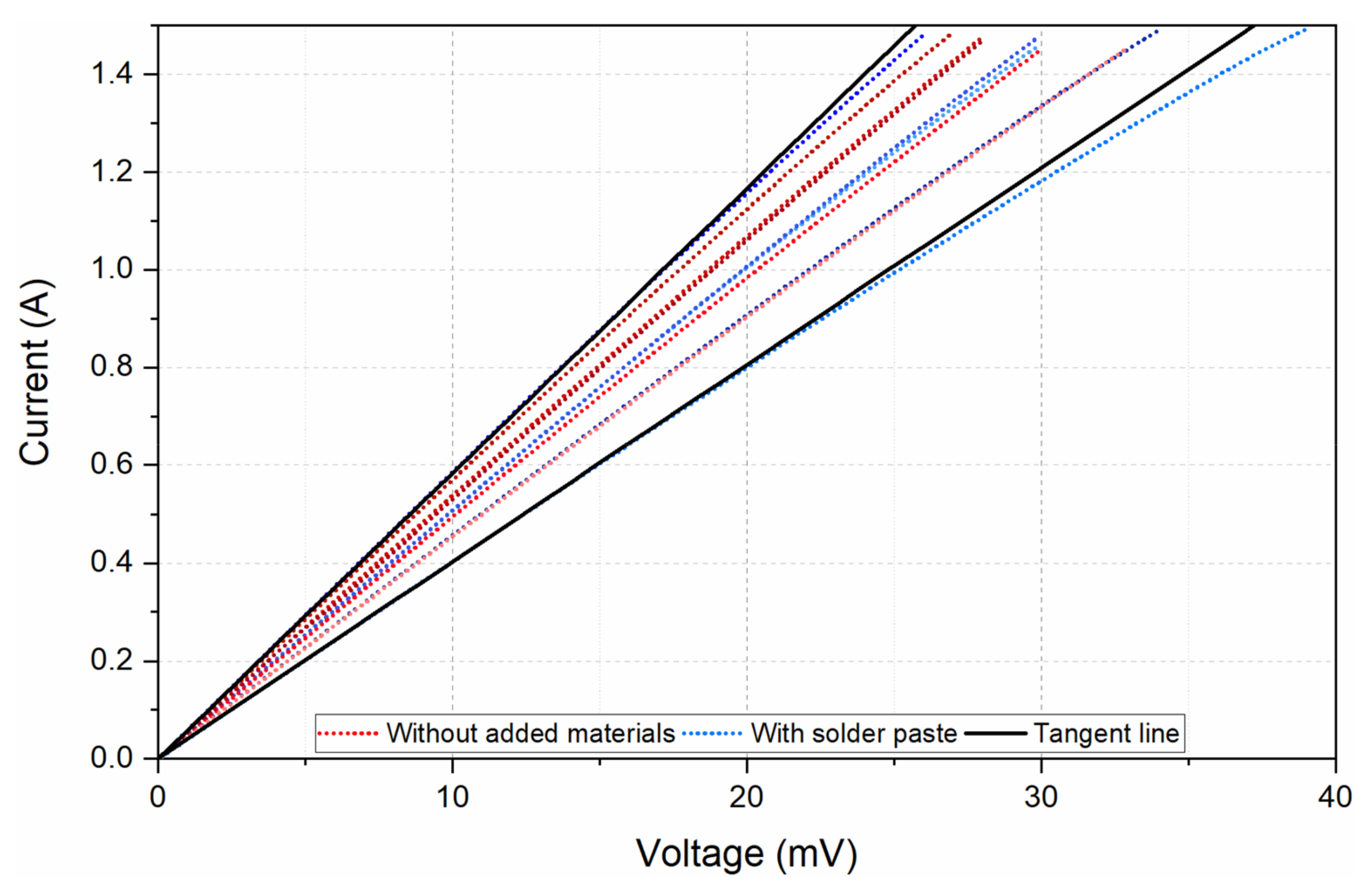
3.3. Voltage–Current Characteristic
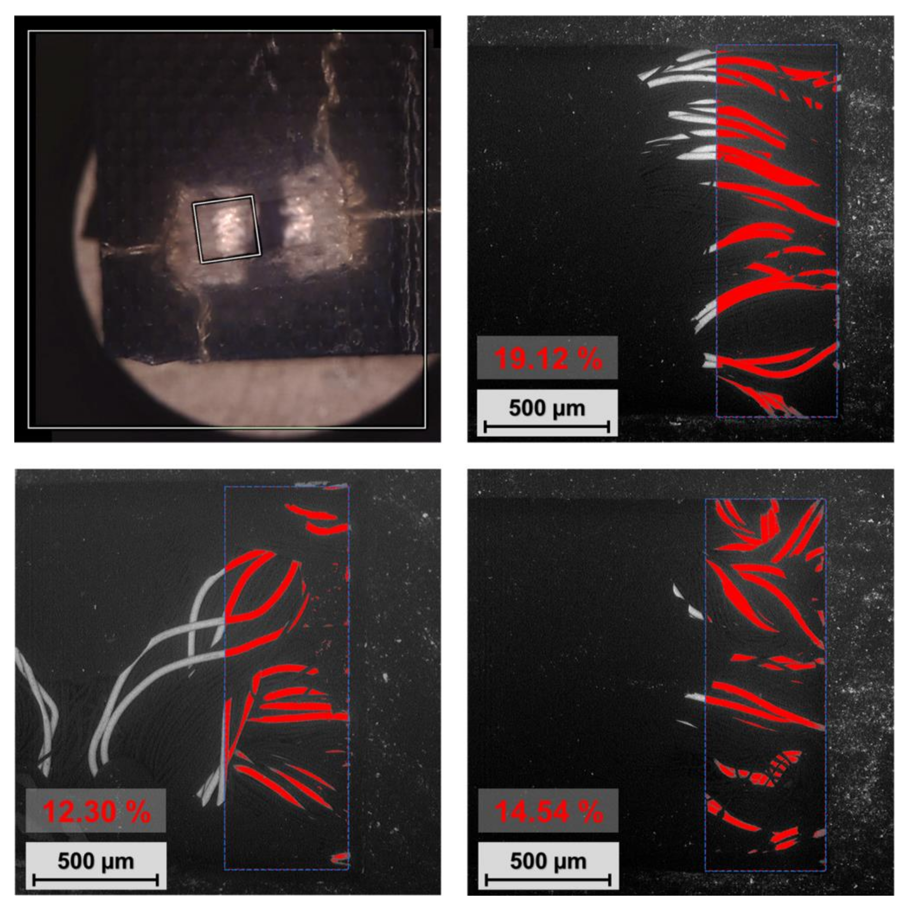
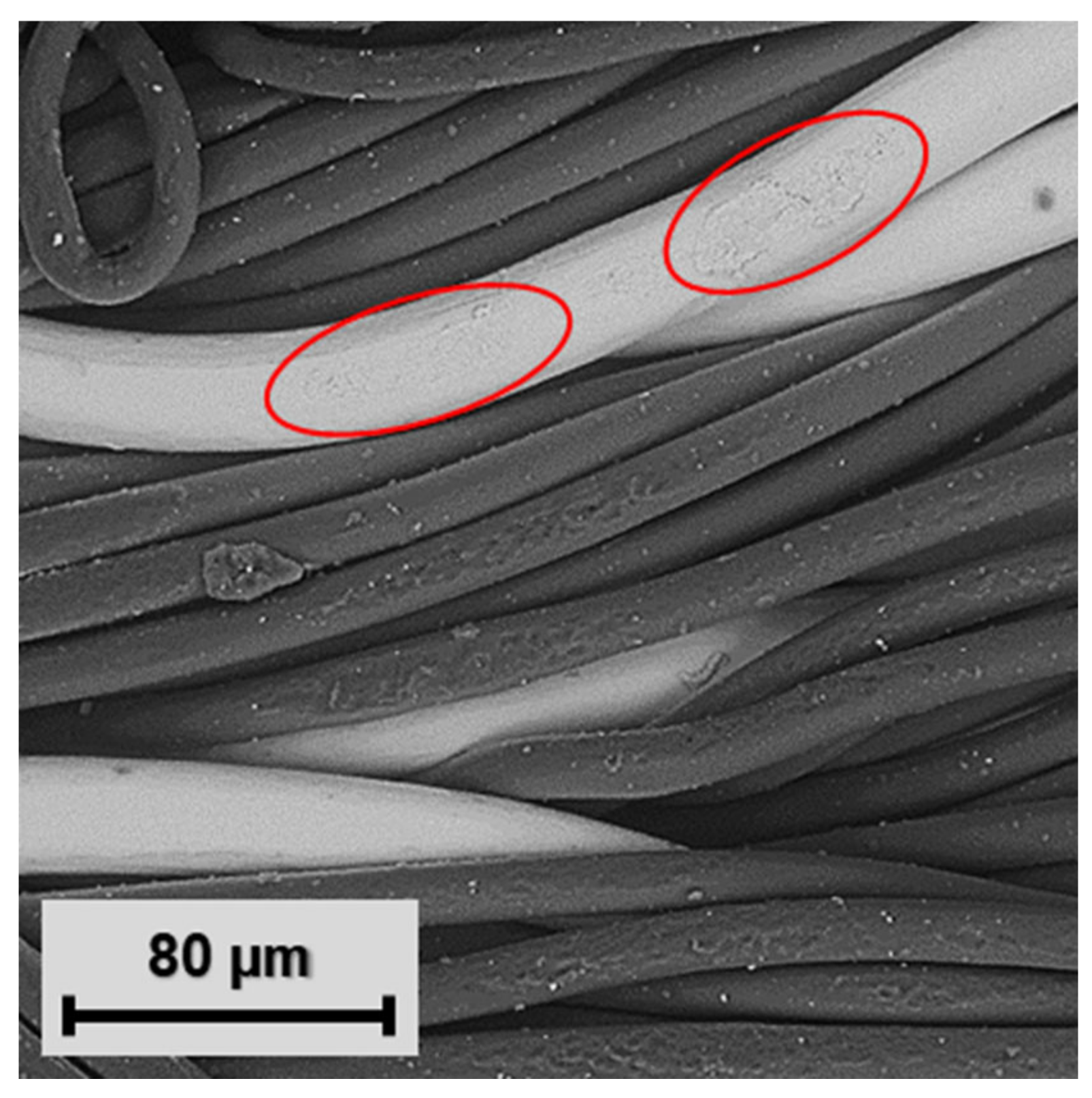
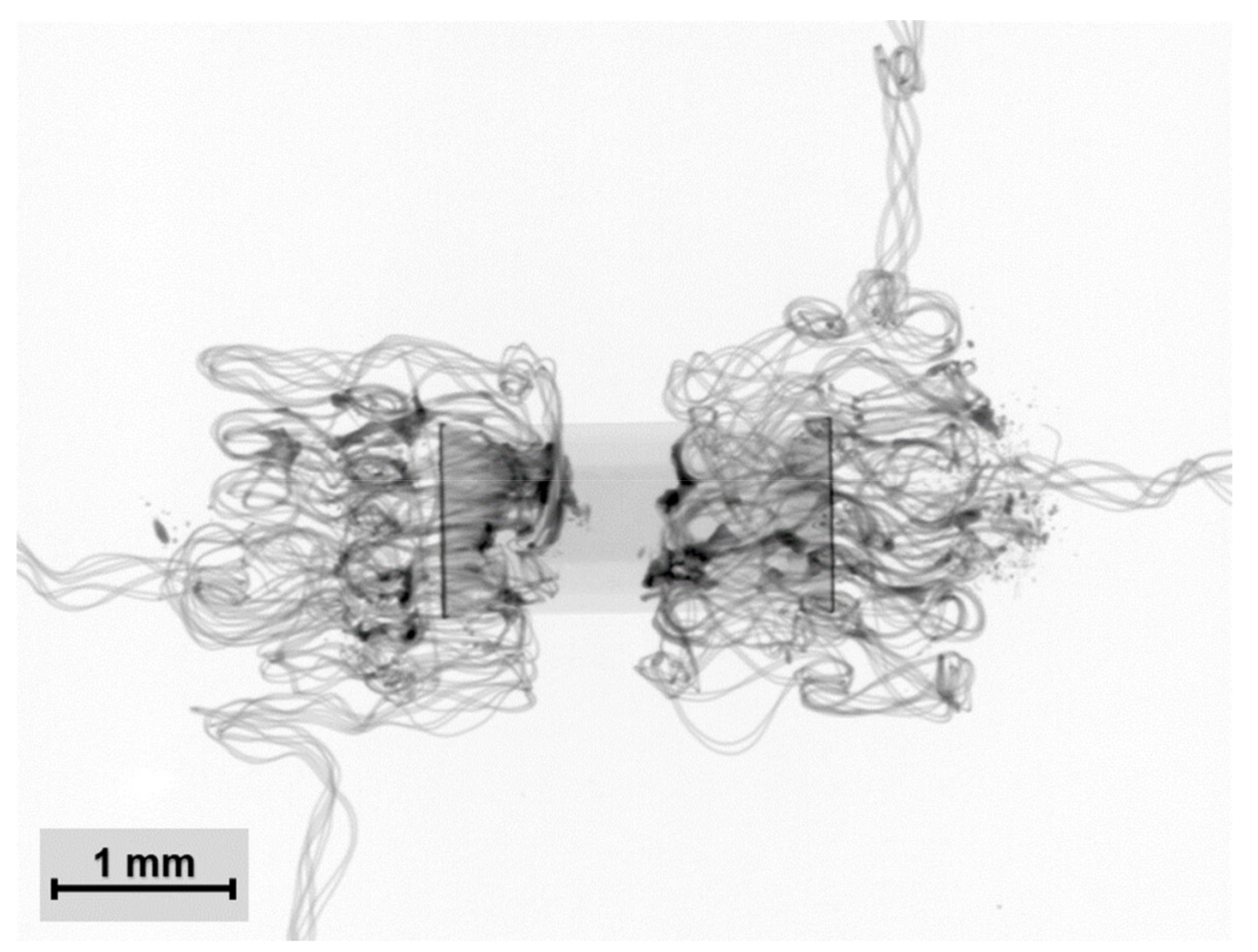
3.4. Electrical Contact Area Analysis
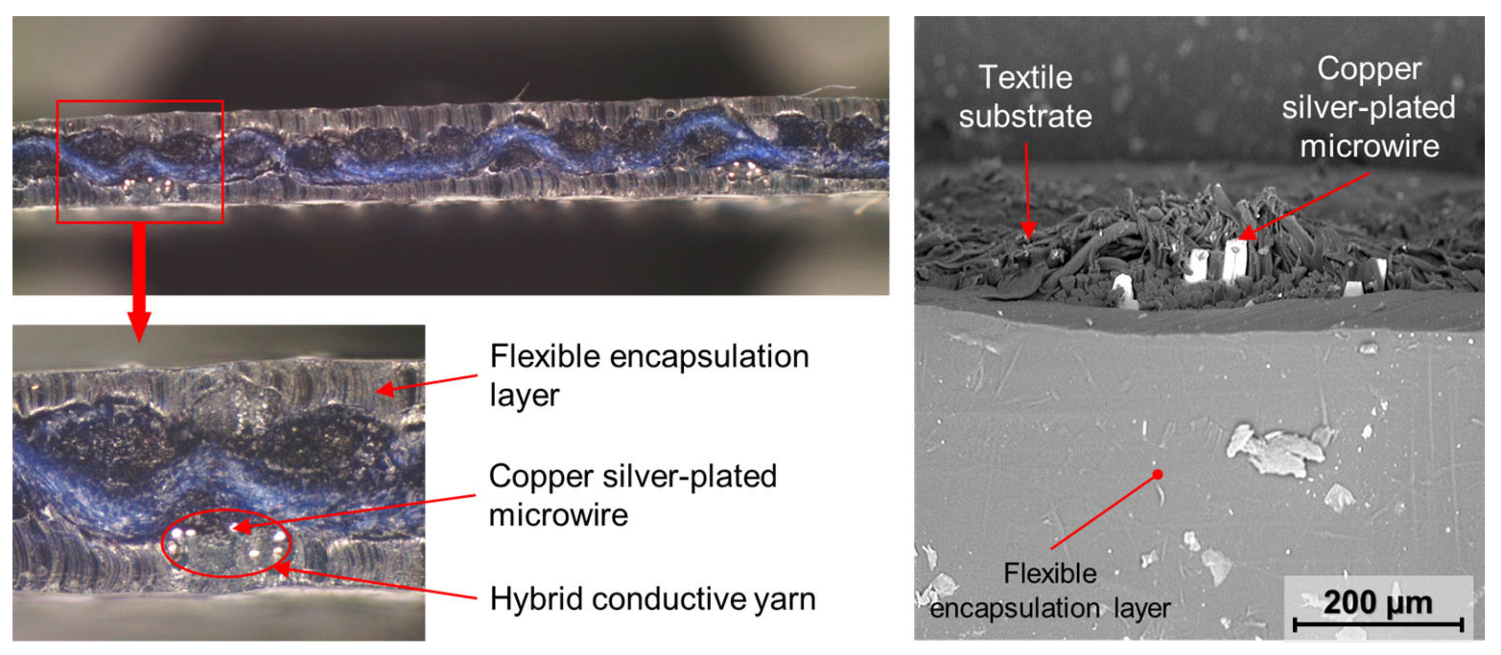
3.5. Optical Inspection of Encapsulation
4. Conclusions
Author Contributions
Funding
Institutional Review Board Statement
Data Availability Statement
Conflicts of Interest
References
- Foster, C.; Rodriguez-Marroyo, J.; de Koning, J. Monitoring Training Loads: The Past, the Present, and the Future. Int. J. Sports Physiol. Perform. 2017, 12, 2–8. [Google Scholar] [CrossRef]
- Taffoni, F.; Rivera, D.; La Camera, A.; Nicolò, A.; Velasco, J.R.; Massaroni, C. A Wearable System for Real-Time Continuous Monitoring of Physical Activity. J. Healthc. Eng. 2018, 2018, 1878354. [Google Scholar] [CrossRef] [PubMed]
- Mattana, G.; Kinkeldei, T.; Leuenberger, D.; Ataman, C.; Ruan, J.J.; Molina-Lopez, F.; Quintero, A.V.; Nisato, G.; Tröster, G.; Briand, D.; et al. Woven Temperature and Humidity Sensors on Flexible Plastic Substrates for E-Textile Applications. IEEE Sens. J. 2013, 13, 3901–3909. [Google Scholar] [CrossRef]
- Skřivan, J.; Blecha, T.; Soukup, R.; Řeboun, J.; Resl, V. Sensors in Textiles for Monitoring Patients with Edema. In Proceedings of the 2018 41st International Spring Seminar on Electronics Technology (ISSE), Zlatibor, Serbia, 16–20 May 2018; pp. 1–5. [Google Scholar]
- Honda, S.; Hara, H.; Arie, T.; Akita, S.; Takei, K. A wearable, flexible sensor for real-time, home monitoring of sleep apnea. iScience 2022, 25, 104163. [Google Scholar] [CrossRef] [PubMed]
- Balaban, J.; Blecha, T. Textile sensor for skin hydration measurement. In Proceedings of the 2022 45th International Spring Seminar on Electronics Technology (ISSE), Vienna, Austria, 11–15 May 2022; pp. 1–5. [Google Scholar]
- Soukup, R.; Blecha, T.; Hamacek, A.; Reboun, J. Smart textile-based protective system for firefighters. In Proceedings of the 5th Electronics System-integration Technology Conference (ESTC), Helsinki, Finland, 16–18 September 2014; IEEE: Piscataway, NJ, USA, 2014; pp. 1–5. [Google Scholar]
- Leigh, S.J.; Bradley, R.J.; Purssell, C.P.; Billson, D.R.; Hutchins, D.A. A Simple, Low-Cost Conductive Composite Material for 3D Printing of Electronic Sensors. PLoS ONE 2012, 7, e49365. [Google Scholar] [CrossRef]
- Repon, M.R.; Mikučionienė, D. Progress in Flexible Electronic Textile for Heating Application: A Critical Review. Materials 2021, 14, 6540. [Google Scholar] [CrossRef] [PubMed]
- Ju, Y.S. Thermal management and control of wearable devices. iScience 2022, 25, 104587. [Google Scholar] [CrossRef]
- Vu, C.C.; Kim, J. Highly Sensitive E-Textile Strain Sensors Enhanced by Geometrical Treatment for Human Monitoring. Sensors 2020, 20, 2383. [Google Scholar] [CrossRef]
- Keum, K.; Cho, S.S.; Jo, J.-W.; Park, S.K.; Kim, Y.-H. Mechanically robust textile-based strain and pressure multimodal sensors using metal nanowire/polymer conducting fibers. iScience 2022, 25, 104032. [Google Scholar] [CrossRef]
- Blecha, T.; Soukup, R.; Kaspar, P.; Hamacek, A.; Reboun, J. Smart firefighter protective suit-functional blocks and technologies. In Proceedings of the 2018 IEEE International Conference on Semiconductor Electronics (ICSE), Kuala Lumpur, Malaysia, 15–17 August 2018; IEEE: Piscataway, NJ, USA, 2018; p. C4. [Google Scholar]
- Du, K.; Lin, R.; Yin, L.; Ho, J.S.; Wang, J.; Lim, C.T. Electronic textiles for energy, sensing, and communication. iScience 2022, 25, 104174. [Google Scholar] [CrossRef]
- Zysset, C.; Cherenack, K.; Kinkeldei, T.; Tröster, G. Weaving integrated circuits into textiles. In Proceedings of the International Symposium on Wearable Computers (ISWC) 2010, Seoul, Republic of Korea, 10–13 October 2010; pp. 1–8. [Google Scholar]
- Kim, S.; Truong, T.; Jang, J.; Kim, J. The Programmable Design of Large-Area Piezoresistive Textile Sensors Using Manufacturing by Jacquard Processing. Polymers 2023, 15, 78. [Google Scholar] [CrossRef]
- Liu, S.; Tong, J.; Yang, C.; Li, L. Smart E-textile: Resistance properties of conductive knitted fabric—Single pique. Text. Res. J. 2017, 87, 1669–1684. [Google Scholar] [CrossRef]
- Gunawardhana, K.R.S.D.; Wanasekara, N.D.; Dharmasena, R.D.I.G. Towards Truly Wearable Systems: Optimizing and Scaling Up Wearable Triboelectric Nanogenerators. iScience 2020, 23, 101360. [Google Scholar] [CrossRef]
- Gaubert, V.; Vauche, G.; Weimmerskirch-Aubatin, J.; Corbier, C.; Boddaert, X.; Delattre, R.; Djenizian, T. Toward autonomous wearable triboelectric systems integrated on textiles. iScience 2022, 25, 105264. [Google Scholar] [CrossRef] [PubMed]
- Truong, T.; Kim, J.-S.; Kim, J. Development of Embroidery-Type Pressure Sensor Dependent on Interdigitated Capacitive Method. Polymers 2022, 14, 3446. [Google Scholar] [CrossRef] [PubMed]
- Stavrakis, A.K.; Simić, M.; Stojanović, G.M. A Study of the Performance Degradation of Conductive Threads Based on the Effects of Tensile Forces and Repeated Washing. Polymers 2022, 14, 4581. [Google Scholar] [CrossRef]
- Tseghai, G.B.; Malengier, B.; Fante, K.A.; Nigusse, A.B.; Van Langenhove, L. Integration of Conductive Materials with Textile Structures, an Overview. Sensors 2020, 20, 6910. [Google Scholar] [CrossRef]
- Zhang, Y.; Wang, H.; Lu, H.; Li, S.; Zhang, Y. Electronic fibers and textiles: Recent progress and perspective. iScience 2021, 24, 102716. [Google Scholar] [CrossRef]
- Ojstršek, A.; Jug, L.; Plohl, O. A Review of Electro Conductive Textiles Utilizing the Dip-Coating Technique: Their Functionality, Durability and Sustainability. Polymers 2022, 14, 4713. [Google Scholar] [CrossRef]
- Kirstein, T. Multidisciplinary Know-How for Smart-Textiles Developers, 1st ed.; Woodhead Publishing: Philadephia, PA, USA, 2013; ISBN 978-0-58709-342-4. [Google Scholar]
- Wills, K.A.; Krzyzak, K.; Bush, J.; Ashayer-Soltani, R.; Graves, J.E.; Hunt, C.; Cobley, A.J. Additive process for patterned metallized conductive tracks on cotton with applications in smart textiles. J. Text. Inst. 2018, 109, 268–277. [Google Scholar] [CrossRef]
- Linz, T.; Simon, E.; Walter, H. Fundamental Analysis of Embroidered Contacts for Electronics in Textiles. In Proceedings of the 3rd Electronics System Integration Technology Conference ESTC, Berlin, Germany, 13–16 September 2010; IEEE: Piscataway, NJ, USA, 2010; p. 5. [Google Scholar]
- Linz, T.; Kallmayer, C.; Aschenbrenner, R.; Reichl, H. Embroidering electrical interconnects with conductive yarn for the integration of flexible electronic modules into fabric. In Proceedings of the Ninth IEEE International Symposium on Wearable Computers (ISWC’05), Osaka, Japan, 18–21 October 2005; pp. 86–89. [Google Scholar]
- Molla, M.T.I.; Goodman, S.; Schleif, N.; Berglund, M.E.; Zacharias, C.; Compton, C.; Dunne, L.E. Surface-Mount Manufacturing for e-Textile Circuits. In Proceedings of the 2017 ACM International Symposium on Wearable Computers, Maui, HI, USA, 11–15 September 2017; Association for Computing Machinery: New York, NY, USA, 2017; pp. 18–25. [Google Scholar]
- Hirman, M.; Navratil, J.; Radouchova, M.; Stulik, J.; Soukup, R. Influence of Sweat on Joint and Sensor Reliability of E-Textiles. Energies 2022, 15, 506. [Google Scholar] [CrossRef]
- Dils, C.; Kalaš, D.; Řeboun, J.; Suchý, S.; Soukup, R.; Moravcová, D.; von Krshiwoblozki, M.; Schneider-Ramelow, M. Interconnecting embroidered hybrid conductive yarns by ultrasonic plastic welding for e-textiles. Text. Res. J. 2022, 92, 4501–4520. [Google Scholar] [CrossRef]
- Tyler, D.J. 17—Joining of wearable electronic components. In Joining Textiles: Principles and Applications; Jones, I., Stylios, G.K., Eds.; Woodhead Publishing: Sawston, UK, 2013; pp. 507–535. ISBN 9781845696276. [Google Scholar]
- Dils, C.; Kallmayer, C.; Gerhold, L.; Schneider-Ramelow, M. Investigations into ultrasonic plastics welding as an innovative contacting technology for the integration of electronics into textiles. Join. Plast. 2020, 14, 104–110. [Google Scholar]
- Michal, D.; Suchý, S.; Josef, Š.; Jan, Ř.; Radek, S. Resistance Welding in Smart Textile. In Proceedings of the 42nd International Spring Seminar on Electronics Technology (ISSE), Wroclaw, Poland, 15–19 May 2019; IEEE: Piscataway, NJ, USA, 2019; p. 6. [Google Scholar]
- Hirman, M.; Navratil, J.; Steiner, F.; Hamacek, A. Reliability of Glued SMD Components on Smart Textile. In Proceedings of the 2020 43rd International Spring Seminar on Electronics Technology (ISSE), Demanovska Valley, Slovakia, 14–15 May 2020; pp. 1–6. [Google Scholar]
- Stanley, J.; Hunt, J.A.; Kunovski, P.; Wei, Y. A review of connectors and joining technologies for electronic textiles. Eng. Rep. 2022, 4, e12491. [Google Scholar] [CrossRef]
- von Krshiwoblozki, M.; Linz, T.; Neudeck, A.; Kallmayer, C. Electronics in Textiles—Adhesive Bonding Technology for Reliably Embedding Electronic Modules into Textile Circuits. Adv. Sci. Technol. 2013, 85, 1–10. [Google Scholar] [CrossRef]
- Joo, H.G.; Jang, Y.H.; Choi, H.S. Electrical Contact Resistance for a Conductive Velcro System. Tribol. Int. 2014, 80, 115–121. [Google Scholar] [CrossRef]
- Cay, G.; Solanki, D.; Al Rumon, M.A.; Ravichandran, V.; Hoffman, L.; Laptook, A.; Padbury, J.; Salisbury, A.L.; Mankodiya, K. NeoWear: An IoT-connected e-textile wearable for neonatal medical monitoring. Pervasive Mob. Comput. 2022, 86, 101679. [Google Scholar] [CrossRef]
- Caldani, L.; Pacelli, M.; Farina, D.; Paradiso, R. E-Textile platforms for rehabilitation. In Proceedings of the 2010 Annual International Conference of the IEEE Engineering in Medicine and Biology, Buenos Aires, Argentina, 31 August–4 September 2010; pp. 5181–5184. [Google Scholar]
- Linz, T.; Kallmayer, C.; Aschenbrenner, R.; Reichl, H. New Interconnection Technologies for the Integration of Electronics on Textile Substrates. In Proceedings of the International Scientific Conference Ambience, Tampere, Finland, 19–20 September 2005; p. 10. [Google Scholar]
- Grimmelsmann, N.; Martens, Y.; Schäl, P.; Meissner, H.; Ehrmann, A. Mechanical and Electrical Contacting of Electronic Components on Textiles by 3D Printing. Procedia Technol. 2016, 26, 66–71. [Google Scholar] [CrossRef]
- Hirman, M.; Navratil, J.; Steiner, F.; Hamacek, A. Effect of Washing Cycles on Glued Conductive Joints Used on Stretchable Smart Textile Ribbons. In Proceedings of the 2020 IEEE 8th Electronics System-Integration Technology Conference (ESTC), Tønsberg, Norway, 15–18 September 2020; pp. 1–4. [Google Scholar]
- Hirman, M.; Navratil, J.; Steiner, F.; Reboun, J.; Soukup, R.; Hamacek, A. Study of low-temperature interconnection techniques for instant assembly of electronics on stretchable e-textile ribbons. Text. Res. J. 2022, 92, 4269–4287. [Google Scholar] [CrossRef]
- Ardebili, H.; Zhang, J.; Pecht, M.G. Encapsulation Technologies for Electronic Applications, 1st ed.; Elsevier: Berkeley, CA, USA, 2019; ISBN 9780128119785. [Google Scholar]
- Kalaš, D.; Šíma, K.; Kadlec, P.; Polanský, R.; Soukup, R.; Řeboun, J.; Hamáček, A. FFF 3D Printing in Electronic Applications: Dielectric and Thermal Properties of Selected Polymers. Polymers 2021, 13, 3702. [Google Scholar] [CrossRef]
- Prusa, J. Chemical Resistance of 3D Printing Materials. Available online: https://prusament.com/chemical-resistance-of-3d-printing-materials/ (accessed on 16 March 2022).
- Rauha, I.; Kauppinen, C.; Liu, Z.; Asikainen, S.; Spoljaric, S.; Seppälä, J.; Savin, H.; Pearce, J. Chemical Compatibility of Fused Filament Fabrication-based 3-D Printed Components with Solutions Commonly Used in Semiconductor Wet Processing. Addit. Manuf. 2018, 23, 99–107. [Google Scholar] [CrossRef]
- Compatible Material List. Available online: https://airwolf3d.com/?ddownload=41151 (accessed on 30 April 2021).
- Prusa Knowledge Base. Available online: https://help.prusa3d.com/en/materials (accessed on 15 February 2021).
- CleverTex Electrically Conductive Hybrid Threads. Available online: https://www.clevertex.cz/en/threads/electrically-conductive-hybrid-threads-detail-761 (accessed on 16 March 2022).
- Sharvin, Y.V. A Possible Method for Studying Fermi Surfaces. J. Exp. Theor. Phys. 1965, 21, 655–656. [Google Scholar]
- Greenwood, J.A. Constriction resistance and the real area of contact. Br. J. Appl. Phys. 1966, 17, 1621–1632. [Google Scholar] [CrossRef]
- Holm, R. Electric Contacts, 4th ed.; Springer: Berlin/Heidelberg, Germany, 1967; ISBN 9783642057083. [Google Scholar]
- Braunovic, M.; Konchits, V.V.; Myshkin, N.K. Electrical Cotnacts: Fundamentals, Applications and Technology, 1st ed.; CRC Press, Taylor & Francis Group: Boca Raton, FL, USA, 2007; ISBN 9781574447279. [Google Scholar]
- Slade, P.G. Temperature of an Electrically Heated a-Spot. In Electrical Contacts: Principles and Applications; CRC Press, Taylor & Francis Group: Boca Raton, FL, USA, 2014; p. 1268. ISBN 9781439881309. [Google Scholar]
- Jeng, Y.-R.; Chiu, S.-M.; Huang, P.-Y.; Shyu, S.-H. Investigation of Thermosonic Wire Bonding Resistance of Gold Wire onto Copper Pad. IEEE Trans. Electron. Packag. Manuf. 2010, 33, 65–70. [Google Scholar] [CrossRef]
- Ding, Y.; Kim, J.-K.; Tong, P. Effects of bonding force on contact pressure and frictional energy in wire bonding. Microelectron. Reliab. 2006, 46, 1101–1112. [Google Scholar] [CrossRef]
- Saiki, H.; Nishitake, H.; Yotsumoto, T.; Marumo, Y. Deformation characteristics of Au wire bonding. J. Mater. Process. Technol. 2007, 191, 16–19. [Google Scholar] [CrossRef]
- Linz, T.; Simon, E.P.; Walter, H. Modeling embroidered contacts for electronics in textiles. J. Text. Inst. 2012, 103, 644–653. [Google Scholar] [CrossRef]


| Technology | Advantages | Disadvantages |
|---|---|---|
| Weaving |
|
|
| Knitting |
|
|
| Embroidering |
|
|
| Interconnection Technology | Advantages | Disadvantages |
|---|---|---|
| Soldering [29,30] |
|
|
| Adhesive bonding [37,43,44] |
|
|
| Ultrasonic welding [32,33] |
|
|
| Sewing [27] |
|
|
| Snap fasteners [41] |
|
|
| Hook and loop strips [25,36] |
|
|
| 3D printing with carbon filled filament [42] |
|
|
| Code | Composition | No. of Microwires | Microwire Diameter [µm] | Basic Yarn Count [Tex] | Yarn Diameter [µm] | Electrical Resistance [Ω/m] | Dry Tensile Strength [cN/Tex] | Dry Elongation [%] |
|---|---|---|---|---|---|---|---|---|
| I-COND art. 74 (Y08) | 24% PES 76% Cu Ag | 8 | 30 | 78 | 240 | 2.85 | 21.85 | 13.3 |
| Microwire Area [%] | Microwire Area [mm2] | Radius of the Appropriated Circular Area [µm] | Theoretical Contact Resistance Rc [mΩ] |
|---|---|---|---|
| 12.30 | 0.095 | 174 | 0.189 |
| 14.54 | 0.113 | 189 | 0.174 |
| 19.12 | 0.148 | 217 | 0.152 |
| Rc [mΩ] | Contact Area [µm2] | Radius of Circular Contact Area [µm] |
|---|---|---|
| 4.5 | 166.4 | 7.27 |
Disclaimer/Publisher’s Note: The statements, opinions and data contained in all publications are solely those of the individual author(s) and contributor(s) and not of MDPI and/or the editor(s). MDPI and/or the editor(s) disclaim responsibility for any injury to people or property resulting from any ideas, methods, instructions or products referred to in the content. |
© 2023 by the authors. Licensee MDPI, Basel, Switzerland. This article is an open access article distributed under the terms and conditions of the Creative Commons Attribution (CC BY) license (https://creativecommons.org/licenses/by/4.0/).
Share and Cite
Kalaš, D.; Soukup, R.; Řeboun, J.; Radouchová, M.; Rous, P.; Hamáček, A. Novel SMD Component and Module Interconnection and Encapsulation Technique for Textile Substrates Using 3D Printed Polymer Materials. Polymers 2023, 15, 2526. https://doi.org/10.3390/polym15112526
Kalaš D, Soukup R, Řeboun J, Radouchová M, Rous P, Hamáček A. Novel SMD Component and Module Interconnection and Encapsulation Technique for Textile Substrates Using 3D Printed Polymer Materials. Polymers. 2023; 15(11):2526. https://doi.org/10.3390/polym15112526
Chicago/Turabian StyleKalaš, David, Radek Soukup, Jan Řeboun, Michaela Radouchová, Pavel Rous, and Aleš Hamáček. 2023. "Novel SMD Component and Module Interconnection and Encapsulation Technique for Textile Substrates Using 3D Printed Polymer Materials" Polymers 15, no. 11: 2526. https://doi.org/10.3390/polym15112526