1. Introduction
Due to the requirements of high-power demand in numerous industrial applications, voltage source converters are used as an alternative in high-power high voltage [
1,
2,
3]. Although many different converter structures are proposed with advantages such as high efficiency, low total harmonic distortion (THD), fault tolerance, and so on [
4,
5], nevertheless, the major aspect of all components used in industrial applications is cost. Therefore, a two-level voltage source inverter (VSI) is a popular converter structure which always competes against the cost of state-of-the-art converter structures due to its simplicity and low-cost requirements [
6,
7]. However, these conventional two-level VSIs have some limitations in operating at high frequency due to corresponding mainly with high switching losses, which decreases the system’s efficiency. Although using low-power loss switching devices is a simple answer, this increases the cost of the converter system. As indicated in literature, the losses of the converter can be classified as conduction and switching losses. Among them, the switching losses are of particular importance since they are the only losses that can be controlled in the modulation stage. By modifying the modulation stage in the control of converter, the switching loss of the converter can be lowered without using additional hardware and increasing the cost of the converter system.
Numerous methods have been extensively developed in the literature to minimize the switching loss and increase the efficiency of converter [
8,
9]. The most known reducing switching loss strategy is based on carrier-based pulse-width modulation (CBPWM) method. By considering a proper zero-sequence voltage injection, discontinuous PWM (DPWM) can be obtained, which can yield low switching losses [
10,
11]. In the most common DPWM methods, the zero-sequence voltage is injected so that reference voltage of one phase is always clamped to the positive or negative dc-rail. The clamped phase is alternated throughout the fundamental cycle. Among several developed DPWM approaches, generalized DPWM (GDPWM) with generalized phase-shift dependent discontinuous modulation waveforms, which capture all of the known discontinuous modulation signals, has been discovered and considered as the most popular strategy [
12,
13]. In GDPWM, the clamping duration per fundamental period does not exceed 120°, and the clamping interval consistently aligns with the peak of the phase current. This strategic positioning effectively decreases the switching losses since they are directly proportional to the current magnitude.
In addition to PWM strategies, there has been extensive research on the use of model predictive control (MPC) for VSI due to its exclusive advantages, including intuitive concepts, a fast dynamic response, and flexible tackling of multiple control objectives and constraints [
14,
15]. Generally, MPC employs a discrete model to predict future system states and applies one optimal switching state obtained by minimizing an objective cost function. Employing a longer sampling time is often the straightforward approach to decrease the switching frequency of MPC [
16]. However, a more precise discrete model is crucial to account for the dynamics of variables accurately. An alternative approach is to limit the available switching states based on the previous switching state of the converter [
17]. Implementing this approach necessitates an additional stage of calculating the possible switching states, which can significantly increase the processing time. A comparable option involves predicting the switching losses and choosing the optimal switching state using either a loss evaluation criterion as described in [
18] or by adding an additional term related to the converter loss in the cost function [
19]. However, determining the appropriate weighting factor for the additional terms is also a challenging task. To overcome these limitations, the authors in [
20] developed a predictive control method with future zero-sequence voltage to reduce switching losses in three-phase VSI. This first MPC scheme (MPC1) modifies the predicted reference voltages using an injected future zero-sequence voltage to generate a clamping interval corresponding to the phase leg with the largest output current. The second MPC scheme (MPC2), developed in [
21], reduces the switching loss of VSI by determining the clamping interval of phase leg using future reference voltages and output currents. Once the optimal clamping interval of phase leg is determined, the possible switching states are selected in a manner that maintains the switching state of a corresponding phase leg.
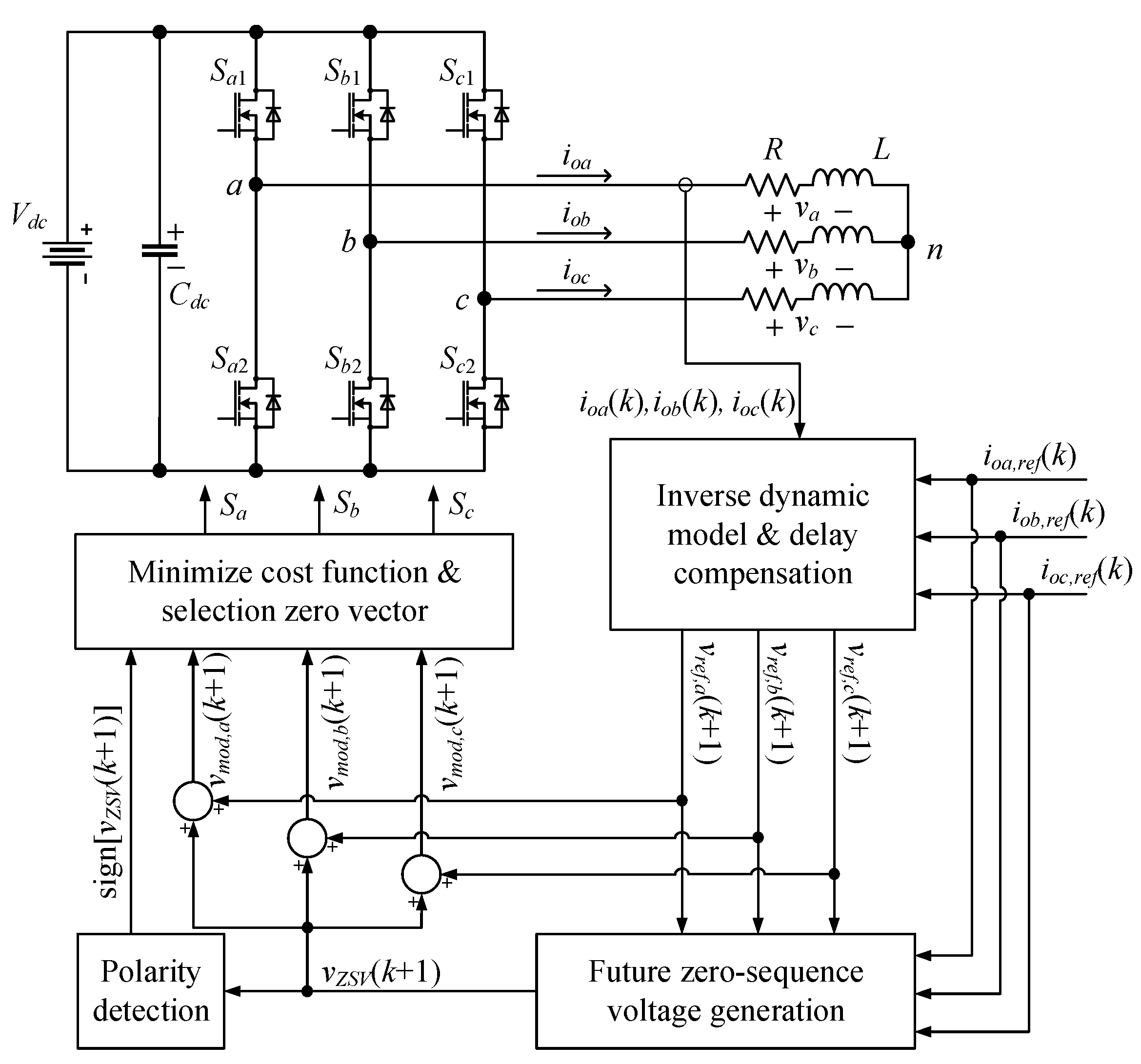
This proposed work investigates a comparative study of the performance of reducing switching loss control schemes, including GDPWN, MPC1, and MPC2 approaches, using in two-level three-phase VSI. The steady-state and transient-state performance have been observed and analyzed during various conditions. In
Section 2, a two-level three-phase VSI system used in simulation and experiment, reducing switching loss control schemes, is presented.
Section 3 presents the simulation and experiment results, as well as output performance comparison under various conditions.
Section 4 concludes this paper.
3. Performance Comparison and Analysis
This section presents the output performance of three-phase VSI acquired by implementing GDPWM, MPC1, and MPC2. The condition for simulation and experiment to analyze the performance of three control schemes are shown the same as in
Table 1. The load angle in this study describes the phase angle difference between voltage and current caused by
load. The simulation is conducted using PSIM simulation program, whereas the experiment is conducted by using the prototype in
Figure 1b.
Concerning the PSIM simulation program, it is specialized software designed for electronic circuit simulation that is primarily used to create power electronics and motor drive simulations, as well as other electronic circuits [
23]. PSIM stands out with its user-friendly graphical interface, simplifying the setup and simulation of intricate power circuits for power electronics engineers. Although MATLAB and PSpice also offer graphical interfaces, they are more commonly used through scripting and coding, which may require greater expertise [
24]. Moreover, PSIM boasts interactive simulation capabilities, enabling users to modify parameter values and observe voltages/currents during simulations. An added advantage of PSIM is its built-in C compiler, allowing users to input C code directly into the program without the need for separate compilation, facilitating the implementation of functions or control methods with ease and flexibility. Additionally, PSIM supports the Thermal Module, enabling the calculation of semiconductor device losses (conduction and switching losses) based on device information from manufacturers’ datasheets.
The principle of MPC method is to select the optimal switching option that minimizes a cost function, and as a result, no commutation is compelled during every sampling period. In fact, a single switching state can serve as the optimal selection for two or more sample periods. This characteristic results in a variable switching frequency. The average switching frequency per power device
will be defined as the average value of the switching frequencies of the six controlled power semiconductor devices in the VSI circuit. Thus
where
is the switching frequency during a time interval of the power semiconductor device number
of phase
. For a fair comparison, the carrier frequency
and sampling frequency
are set to achieve similar average switching frequency in both GDPWM and MPC methods.
Figure 6 illustrates the output current waveforms and corresponding switching patterns at steady state obtained by the GDPWM, MPC1, and MPC2 methods in both simulation and experiment. The output currents acquired through three control schemes exhibit sinusoidal waveforms and demonstrate accurate magnitude and phase. Both GDPWM and MPC methods are capable of tracking the reference current. The phase
output current
obtained by three control schemes shows a negligible deviation from the corresponding reference current
, as shown in
Figure 6a–c. As can be seen from the switching patterns of three-phase legs, all three approaches have similar non-switching intervals in each phase, where each phase is clamped to either the positive or negative dc-rail for
in one fundamental period.
Regarding the dynamic performance,
Figure 7 illustrates the output current waveforms at transient-state obtained by the GDPWM, MPC1, and MPC2 methods in simulation and experiment. The transient state is generated by applying an abrupt change in the magnitude of reference current from
to
. It should be noted that as the PI controller in the GDPWM method requires enough time to achieve the first steady state corresponding to
of magnitude of reference current, this means that the output current correctly follows the output current reference. Therefore, the left-hand side figure in
Figure 7 has the origin of time not equal to zero. In this manner, the dynamic performance of the output current can be evaluated. It can be seen that in
Figure 7b,c, the MPC methods exhibit superior dynamic performance where the output current immediately changes its magnitude following the change of corresponding reference current with a negligible overshoot in both simulation and experiment results. Meanwhile, the GDPWM method requires more time to achieve the change of reference current. Thus, transient-state performance of MPC methods is better than the GDPWM approach with less settling and rise time, which are required to achieve the desired set point.
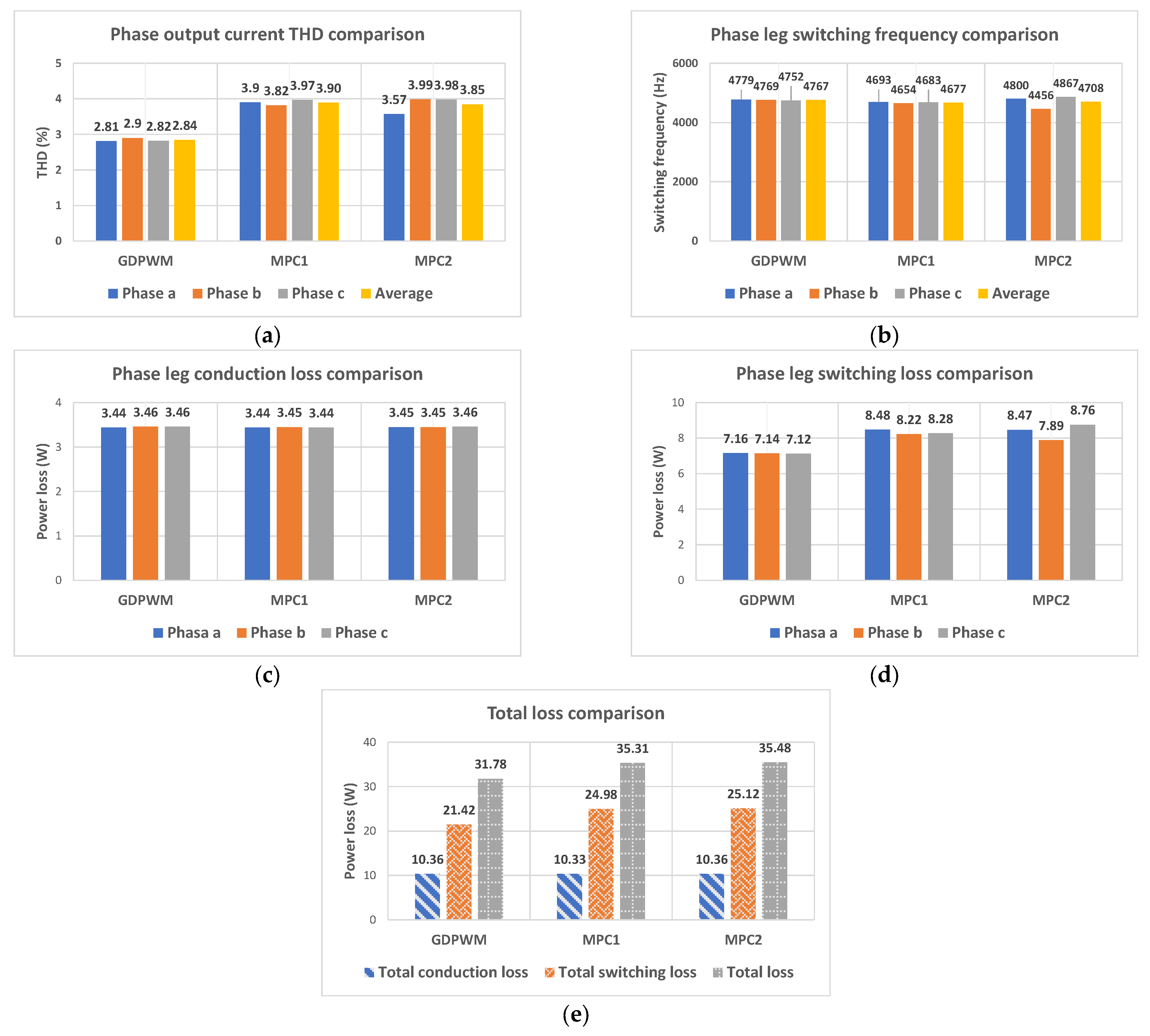
The calculated values from simulation results are presented to thoroughly assess output performance, switching frequency, and switching loss reduction capability obtained by the GDPWM, MPC1, and MPC2 methods. The power losses are calculated by the thermal module in the PSIM simulation program by using parameters from the IGBT module’s datasheet (Semikron SK60GM123).
Figure 8a–e illustrate the performance comparison between GDPWM, MPC1, and MPC2 methods regarding switching frequency, output current THD, and power losses. As indicated earlier, the switching frequency and sampling frequency are set to achieve a comparable average switching frequency obtained by three control schemes. As shown in
Figure 8a, the phase and average switching frequencies acquired by GDPWM, MPC1, and MPC2 approaches are similar. The comparable average switching frequency is achieved at approximately 4.7 kHz. In
Figure 8b, the phase and average switching frequencies obtained by three control schemes are presented. It can be realized that the GDPWM method generates output currents with the lowest THD value. Meanwhile, the MPC1 and MPC2 approaches have higher average THD than that of GDPWM by about 37% and 35%, respectively. The difference of output current THD between MPC and MPC2 methods is negligible. Regarding the power loss performance,
Figure 8c–e show that the three control schemes have similar conduction loss. The two MPC approaches also have similar switching loss and total loss, but the GDPWM shows lower switching loss compared to the two MPC approaches. The two MPC approaches have higher total switching loss and total loss than that of GDPWM by about 16% and 11%, respectively.
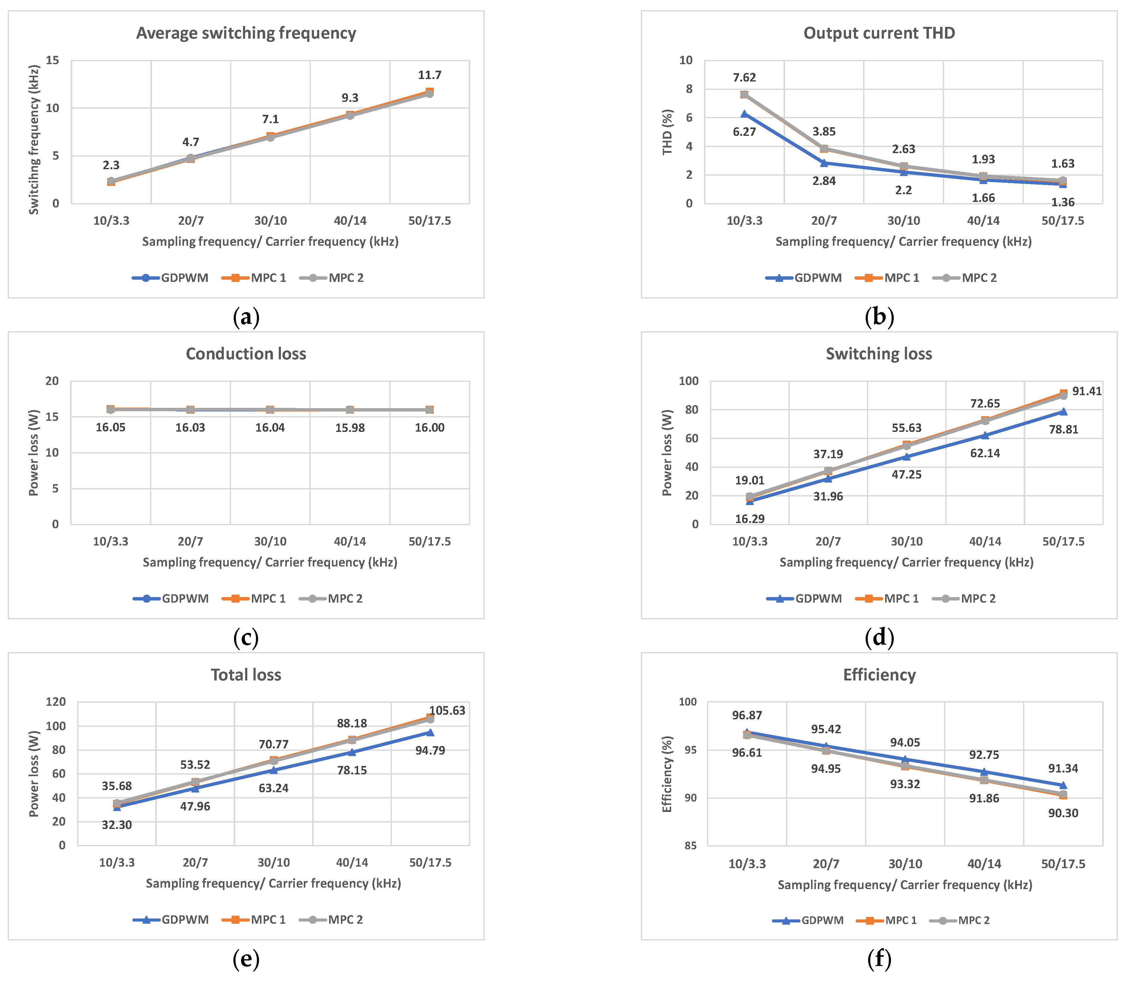
To further assess the performance between GDPWM, MPC1, and MPC2 methods, the comparison among three methods is conducted under various conditions, including different switching frequencies, different output powers, and different load conditions. First, the output performance comparison is conducted under different switching frequency conditions. As shown in
Figure 9a, the carrier frequency in GDPWM method and sampling frequency in MPC methods are increased to change the switching frequency. It should be noted that the carrier and sampling frequencies are adjusted to achieve similar average switching, as shown in
Figure 9a. Thanks to the increase in switching frequency, the average current THD decreases. It can be seen in
Figure 9b that the average output current THD obtained by three methods decreases following the rise of switching frequency. It can be noticed that the output current obtained by two MPC methods is higher than that of GDPWM. The difference in output current THD between GDPWM method and two MPC methods ranges from 20% to 35%. Because the conduction loss is not affected by the switching frequency, the conduction obtained by GDPWM and two MPC methods is similar. Meanwhile, the switching loss and total loss increases following the rise of switching frequency. The two MPC approaches have higher switching loss and total loss compared to that of GDPWM by about 16% and 11%, respectively. Thus, GDPWM has slightly higher efficiency than the two MPC methods, as shown in
Figure 9f.
The output performance comparison, conducted under different output power conditions, is shown in
Figure 10a–f. As shown in
Figure 10a, the carrier frequency in GDPWM method and sampling frequency in MPC methods are adjusted to achieve similar average switching following the variation of output power condition. Following the increase of output power, the average current THD obtained by three control schemes decreases. It can be seen in
Figure 10b that the average output current THD obtained by three methods decreases following the rise of output power. It can be noticed that the output current obtained by two MPC methods is higher than that of GDPWM. The difference of output current THD between GDPWM method and two MPC methods ranges from 10% to 35%. Because the conduction loss is not affected by the switching frequency, the conduction obtained by GDPWM and two MPC methods are similar, as shown in
Figure 10c. However, due to the increase in output power, the corresponding conduction loss increases as well. Meanwhile, the switching loss and total loss increase following the rise of output power. The difference in switching loss between the two MPC methods and GDPWM method decreases when the output power increases. This difference is highest at 1 kW output power of 26%, while it is lowest at 10 kW output power of about 10%, as shown in
Figure 10d. Consequently, the difference of total loss between the two MPC methods and GDPWM method decreases when the output power increases. This difference ranges from 5% to 13% depending on the output power conditions, as shown in
Figure 10e. In terms of efficiency, the GDPWM method has slightly higher efficiency than the two MPC approaches.
Figure 11a–f illustrate the comparison of output performance under various load conditions. To modify the phase angle, the output inductance of the VSI is increased. As shown in
Figure 11a, the carrier frequency in GDPWM method and sampling frequency in MPC methods are appropriately adjusted to achieve similar average switching following the variation of load condition. Following the increase of load phase angle, the average current THD obtained by three control schemes decreases significantly. It can be seen in
Figure 11b that the average output current THD obtained by three methods decreases following the rise of load phase angle. It is noticed that the output current obtained by two MPC methods is higher than that of GDPWM. The difference of output current THD between GDPWM method and two MPC methods decreases following the increase of phase angle. Additionally, this difference is slight. Because the conduction loss is not affected by the switching frequency, the conduction obtained by GDPWM and two MPC methods are similar, as shown in
Figure 11c. Simultaneously, the switching loss and total loss experience a relative increase as the load phase angle rises. As the load phase angle increases, the difference in switching loss between the two MPC methods and the GDPWM method diminishes. This difference is highest at
load phase angle of about 33%, while it is lowest at
load phase angle of about 10%, as shown in
Figure 11d. As a result, the contrast in total loss between the two MPC methods and the GDPWM method diminishes with an increase in the load phase angle. The variation in this distinction ranges from 6% to 11%, varying following the conditions of the load phase angle, as depicted in
Figure 11e. In terms of efficiency, the GDPWM method has slightly higher efficiency than the two MPC approaches.
The PWM method does not require the information of load, so it is not affected when a parameter mismatch of load or even an unbalanced load exists. Meanwhile, the load information is crucially required for the prediction model. The behavior of MPC1 and MPC2 methods under parameter mismatch of load inductance, including various performances such as average THD, %error of output current, average switching frequency, and total loss, are shown in
Figure 12a–d. The horizontal axis of line charts in
Figure 12 presents the difference between the model parameter inductance and the actual inductance. As shown in
Figure 12a, the output current THD acquired by the MPC2 method is maintained well under load inductance error. The output current THD obtained by the MPC1 method increases considerably when the load inductance error exceeds 35%. In
Figure 12b, the %error of output current obtained by the MPC1 significantly increases by about 60% when the load inductance error is 50%. The %error of output current obtained by the MPC2 significantly increases when the model parameter inductance is lower than the actual inductance. Meanwhile, when the model parameter inductance is higher than the actual one, the %error of output current obtained by the MPC2 method slightly decreases. When the model parameter inductance is lower than the actual one, the MPC1 method has a similar average switching frequency. However, when the model parameter inductance is higher than the actual one, the average switching frequency decreases. This leads to the reduction of total loss obtained by the MPC1 method, as shown in
Figure 12d. Contrastingly, the average switching frequency of MPC2 method decreases when the model parameter inductance is lower than the actual one and vice versa.
The behavior of MPC1 and MPC2 methods under parameter mismatch of load resistance, including various performances such as average THD, %error of output current, average switching frequency, and total loss, are shown in
Figure 13a–d. The horizontal axis of the line charts in
Figure 13 presents the difference between the model parameter resistance and the actual resistance. As shown in
Figure 13a, the output current THD obtained by two MPC methods is maintained well under load resistance error. The output current THD slightly changes, even when the load resistance error is 50%. In
Figure 13b, the %error of output current obtained by the MPC1 significantly increases by about 60% when the load resistance error is 50%. The %error of output current obtained by the MPC2 slightly increases when the model parameter resistance is lower or higher than the actual resistance. In case the model parameter resistance is lower than the actual one, the average switching frequency obtained by two MPC methods increases, while the average switching frequency slightly decreases when the model parameter resistance is higher than the actual one. As for total power loss, the total loss of MPC1 method increases in the case that the load resistance error is higher than 35%. Meanwhile, the MPC2 method maintains a similar total loss when the model parameter resistance is higher than the actual one. It can be realized that the effect of load resistance mismatch is lower than the load inductance mismatch.
The behavior of MPC1 and MPC2 methods under parameter mismatch of load resistance, including various performances such as average THD, %error of output current, average switching frequency, and total loss, are shown in
Figure 13a–d. The horizontal axis of the line charts in
Figure 13 presents the difference between the model parameter resistance and the actual resistance. As shown in
Figure 13a, the output current THD obtained by two MPC methods is maintained well under load resistance error. The output current THD slightly changes, even when the load resistance error is 50%. In
Figure 13b, the %error of output current obtained by the MPC1 significantly increases by about 60% when the load resistance error is 50%. The %error of output current obtained by the MPC2 slightly increases when the model parameter resistance is lower or higher than the actual resistance. In case the model parameter resistance is lower than the actual one, the average switching frequency obtained by two MPC methods increases, while the average switching frequency slightly decreases when the model parameter resistance is higher than the actual one. As for total power loss, the total loss of MPC1 method increases in case the load resistance error is higher than 35%. Meanwhile, the MPC2 method maintains a similar total loss when the model parameter resistance is higher than the actual one. It can be realized that the effect of load resistance mismatch is lower than the load inductance mismatch.


