Study of Brush-Painted Ag Nanowire Network on Flexible Invar Metal Substrate for Curved Thin Film Heater


1
School of Advanced Materials Science and Engineering, Sungkyunkwan University, Suwon, Gyeonggi-do 16419, Korea
2
Department of Fine Arts, Sungkyunkwan University, 25-2, Sungkyunwan-ro, Jongno-gu, Seoul 03063, Korea
*
Author to whom correspondence should be addressed.
Metals 2019, 9(10), 1073; https://doi.org/10.3390/met9101073
Submission received: 9 September 2019
/
Revised: 25 September 2019
/
Accepted: 30 September 2019
/
Published: 2 October 2019
Abstract
:The objective of this study was to determine the characteristics of brush-painted Ag nanowires (NW) network electrode on a SiO2 coated invar substrate for high performance curved thin film heaters (TFHs). To avoid influence of a conductive invar metal foil substrate, thin SiO2 film was deposited on an invar substrate as an insulating layer. We measured sheet resistance, optical reflectance, and surface morphology of Ag NWs/SiO2/invar as a function of the number of brush painting from one to four times. Optimized brush-painted Ag NWs network on a SiO2/invar substrate showed a low sheet resistance 38.52 Ω/square, which was acceptable for fabrication of curved TFHs. Based on a lab-made bending and fatigue tester, critical radius of the optimized Ag NWs/SiO2/invar electrode was found to be 6 mm. It demonstrated superior repeated flexibility of an Ag NW/SiO2/invar substrate. Furthermore, we demonstrated the feasibility of using a brush-painted Ag NW/SiO2/invar substrate as an electrode for curved TFHs. These curved TFHs fabricated on an Ag NW/SiO2/invar substrate showed rapid heating properties and high saturation temperature even at low applied voltage due to low resistivity of Ag NW network. This indicates that a brush-painted Ag NW/SiO2/invar substrate is a promising flexible electrode and substrate for high performance curved TFHs.
1. Introduction
Joule heat based thin film heaters (TFHs) have been investigated for various device applications. For successful manufacturing of TFHs, it demands a high quality electrode with a low resistivity and outstanding mechanical flexibility [1,2]. To meet the requirements of the TFHs, different kinds of electrode materials such as graphene, carbon nanotube, metal nanowire, conductive oxide, and hybrid electrodes have been employed [3,4,5,6,7,8,9]. Among them, Ag nanowire (NW) network was extensively employed as an electrode material due to its merits such as a solution-based simple coating process, a low resistivity, a high optical transmittance, and outstanding mechanical properties [10]. Although the Ag NW network electrode was used as a Joule heating layer for TFHs, which fabricated on a polymer or glass substrates [11,12,13,14], the effectivity of flexible or curved TFHs that is fabricated on an Ag NW coated metal foil substrate was not reported until now. Metal foil substrates have many advantages, including a low coefficient of thermal expansion (CTE), chemical stability, and mechanical stability. Kim et al. [15,16,17] have reported the feasibility of using a flexible metal foil substrate for flexible solar cells and shown the advantage of the metal foil substrate. An organic light emitting device (OLED) and amorphous Si thin-film transistors fabricated on a metal foil substrate have been reported by Wu et al. [18]. Invar metal foil, one of metal foils developed by Guillaume in 1897, has lower CTE and better chemical stability than other metal foils [19,20,21,22,23]. For those reasons, an invar metal foil substrate has been employed in flexible OLED [24]. We have also reported the possibility of using an invar metal foil substrate for flexible perovskite solar cells [25]. Although invar metal foil has been used as flexible OLED and solar cells, detailed investigation of brush-painted Ag NW on an invar substrate for flexible thin film heater is not developed yet. Recently simple printing processes, such as spin-coating, bar-coating, ink-jet, and brush-painting, have been paid much attention due to their handiness, rapidity, and affordability [26,27]. Among them, the brush-painting process is one of the most simple printing processes because it requires only simple tools like a painting brush and functional ink [28]. Specially, it can control film thickness from ~10 nm to a few hundred nanometers and form polymer chains or one-dimensional nanostructure layers by shear stress. In addition, it can be applied onto various flat and textured substrates [28]. Kim et al. [29,30,31,32] have successfully reported the possibility of a fabricating organic thin film transistor and perovskite solar cells by means of the brush painting process. We have also reported a successful fabrication of conductive electrode for organic solar cells based on the following materials: Ag nanowires (NW), poly(3,4-ethylenedioxylenethiophene):poly(styrene sulfonic acid) (PEDOT:PSS), Ti-doped In2O3 nanoparticles, and Sn-doped In2O3 nanoparticles [33,34,35,36,37]. Furthermore, we have successfully fabricated brush-painted stretchable electrode based on a polyurethane substrate by means of a composite of Ag NWs and PEDOT:PSS [28]. Therefore, brush-painted Ag NW on an invar substrate will able to play a significant role as a conductive electrode for curved TFHs.
In this study, we investigated the electrical, optical, morphological, and mechanical properties of brush-painted Ag NWs network on an invar metal foil substrate to show its feasibility for curve TFHs. The effects of brush painting times on sheet resistance and reflectance of Ag NW/SiO2/invar substrates were also determined. In addition, we investigated the mechanical flexibility and repeated fatigue properties of an optimized Ag NW/SiO2/invar substrate. Moreover, we fabricated curved TFH on the optimized Ag NW/SiO2/invar substrate and investigated heating performance of these curved TFHs. Based on heating theory, we investigated the thermal properties of curved TFHs on the Ag NWs/SiO2/invar substrate and showed the feasibility of fabricating brush painted Ag NW network on the invar substrate.
2. Materials and Methods
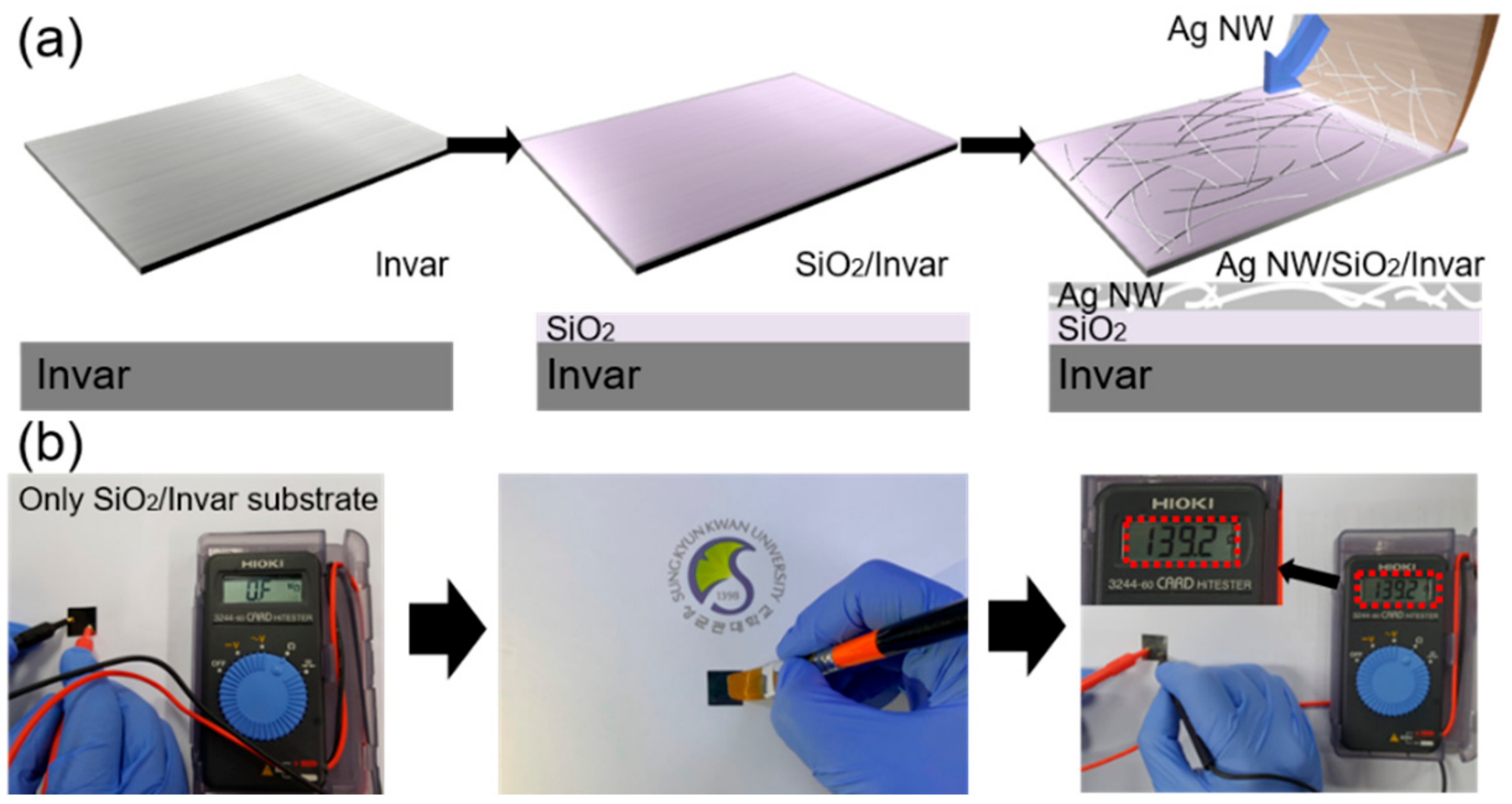
Figure 1a shows the process of fabricating flexible Ag NW electrode on an invar metal foil substrate. We employed a general invar metal foil (36%Ni–64%Fe) substrate supported by Pohang Iron & Steel Company(POSCO). On the invar metal foil substrate, we deposited the SiO2 insulating layer to demonstrate that the electrical conductivity of the Ag NW electrode was not affected by the invar metal substrate. Then a 2 μm thick SiO2 insulating layer was deposited on the invar metal substrate using commercial plasma enhanced chemical vapor deposition (PECVD). Ag NWs (N&B Co., Ltd., average 25 µm length, 25 nm diameter) were then directly brush-painted on a SiO2 coated invar substrate with the increasing number of brush strokes from one to four times using a commercial painting brush (ROYAL 2580 KORF, 5). Due to the small sample size of the brush, we could prepare a uniformly coated Ag NW network through simple brush strokes at room temperature. Figure 1b shows the effect of 2 μm thick SiO2 insulating layer before coating of the Ag NW layer. The 2 μm thick SiO2 layer effectively prevented current path through the invar metal substrate. After Ag NW brush painting on the SiO2 coated invar substrate, the Ag NW layer had conductivity as shown in Figure 1b (right).
To analyze the electrical and optical properties of the brush-painted Ag NWs/SiO2/invar metal substrate as a function of the number of brush strokes we used 4-point-probe (FPP-HS B, DASOL ENG) and UV/visible spectrometer (UV 540, Unicam). With a field emission scanning electron microscope (FESEM; JSM-7600F), we investigated the surface morphology of a brush-painted Ag NWs/SiO2/invar metal substrate. The mechanical properties of the brush-painted Ag NWs/SiO2/invar metal substrate were examined with a lab-designed outer and inner bending test machine. We measured the resistance change of the Ag NWs/SiO2/invar metal substrate with in-situ, while bending the samples. To show the feasibility of using a brush-painted Ag NWs/SiO2/invar metal substrate for curved TFHs, we fabricated curved TFHs on the Ag NWs/SiO2/invar metal substrate with a size of 2.5 × 2.5 cm2. We used Cu tape on the two terminal sides of the Ag NWs/SiO2/invar metal substrate as a contact electrode. We measured the temperatures of TFHs as a function of input voltage and heating and cooling cycling times. To apply direct current (DC) power to curved TFHs, a power supply (OPS 3010, ODA technologies) was employed through the Ag contact electrode. The temperatures of the curved TFHs were measured by means of a thermocouple that directly touches on the surface of TFHs and an IR thermal image cameral (A35sc, FLIR).
3. Results and Discussion
Figure 2a shows the contact angle of water and isopropyl alcohol (IPA) on a SiO2/invar substrate, since water is less affinitive than the IPA solvent on the SiO2 coated invar substrate, the water based-Ag NWs layer is easily agglomerated before evaporation water solvent, leading to ununiform coating of Ag NW layer [38]. However, IPA and water mixed solvent based Ag NW showed a uniform coating due to lower contact angle (14.9°) than that (27.6°) of water based Ag NW ink. Figure 2b shows the comparison of ink droplet and the Ag NW layer after drying solvent. Due to the different surface energies of water based and water–IPA mixed solvent based Ag NW inks, the Ag NWs coated from water–IPA mixed solvent showed a more uniform Ag NW network layer than Ag NW from the water-based Ag ink. Therefore, we carried out the brush painting process on the SiO2 coated invar metal substrate with Ag NWs solution with water–IPA mixing ratio of 1:2 (0.3 wt% Ag NWs water solution:IPA solution).
Figure 3a shows sheet resistances and the picture of the brush-painted Ag NWs network electrode on a SiO2 coated invar metal substrate with the increasing number of brush strokes. Ag NW network formed by one time of brush painting process showed a fairly high sheet resistance of 98.04 Ω/square with large error scale bar due to ununiform connection between Ag NWs as confirmed by surface FESEM image (Figure 3b). However, Ag NW network formed by two times of brush painting process exhibited significantly reduced sheet resistance of 38.62 Ω/square due to improved connectivity of the Ag NWs. Further increase in brush painting times led to a gradual decrease in a sheet resistance. Figure 3b shows surface FESEM images of brush painted Ag NWs network electrode according to the number of brush painting. As expected from sheet resistance, increasing number of brush painting increased Ag NW density, which is critically affected on the sheet resistance. In addition, connectivity between Ag NWs was improved by shear stress of the brush [28,30,31]. Based on sheet resistance of the Ag NW network electrode and surface morphology shown in picture, the optimal number of brush painting processes was found to be 2.
Figure 4a shows optical reflectance of brush-painted Ag NWs network on SiO2 coated invar metal substrate according to increase in the number of brush painting. Due to high reflectance of the SiO2/invar metal substrate and high optical transmittance of Ag NW network, the brush painted Ag NW showed similar optical reflectance with bare SiO2/invar metal substrate regardless of brush painting times. Nevertheless, when the number of brush painting process increased, the reflectance of the Ag NWs/SiO2/invar metal substrate slightly decreased due to decreased optical transmittance of Ag NW with increasing density. Figure 4b shows reflection of SKKU logo from the surface of Ag NWs/SiO2/invar metal substrate.
To apply an Ag NWs/SiO2/invar metal substrate onto curved TFHs, the mechanical flexibility of Ag NW network electrode is extremely significant. To show a good flexibility of the brush-painted Ag NW network, we conducted an inner and outer bending radius test with a lab-designed bending test machine. Inner and outer radius in the bending radius test means the radius of the concave and convex direction of the Ag NWs/SiO2/invar metal substrate samples as shown in Figure 5a. In the case of the inner radius bending test, Ag NWs network electrode experienced a compressive stress at the center of Ag NWs network electrode. By contrast, in the outer radius bending test, Ag NWs network electrode experienced tensile stress. Figure 5b shows the result of the radius bending test that defined a critical radius (left); and the result of the dynamic fatigue test that demonstrated mechanical stability (right). The critical radius was defined when the resistance change of the brush-painted Ag NWs network electrode occurred by the disconnection of Ag NWs or peeling-off of the 2 µm thick SiO2 layer from the invar metal substrate. Inset pictures show the steps of the bending radius test and dynamic fatigue radius test, respectively. During the inner and outer radius test, we continued to measure the resistance change of the brush-painted Ag NW electrode, while decreasing bending radius. The resistance change can be expressed as (R − Ro)/Ro, where Ro is the initial resistance, and R is the simultaneously measured resistance under substrate bending [28,33,35,39,40]. The inner and outer bending radius test showed that the two optimized brush strokes onto Ag NWs network electrode had a constant resistance until the inner radius was 4 mm and outer radius was 6 mm. When the radius was higher than the critical radius, resistance increased due to the disconnection of Ag NWs and SiO2 exfoliation. Based on these inner and outer bending radius tests, the safe dynamic bending radius was chosen to be 8 mm. Therefore, we conducted the dynamic fatigue test, while increasing the number of bending cycles at a fixed outer and inner bending radius (8 mm). Both tests showed constant resistance during 10,000 cycles, indicating superior mechanical flexibility of the brush-painted Ag NWs network electrode. Figure 5c shows the surface FESEM image of the Ag NWs electrode after the inner and outer dynamic fatigue tests, respectively. Considering curvature of curved TFHs, the small critical bending radius and superior mechanical flexibility, the brush-painted Ag NW on SiO2/invar metal substrate is acceptable to fabricate curved TFHs.
Figure 6 shows a promising application of brush-painted optimized (twice brush-painted) Ag NW network electrode on a SiO2 coated invar metal substrate in curved TFHs. Figure 6a shows the process of fabricating TFH and the temperature measurement method of the TFH. To apply voltage effectively to the Ag NW network, we used copper tape at the edge of the Ag NWs/SiO2/invar metal substrate as contact electrodes. We then applied voltage for 400 s for each voltage from 4 V to 8 V and directly mounted a thermocouple on the surface of the Ag NWs/SiO2/invar metal substrate.
Figure 6b shows temperature profile of Ag NW network based curved TFHs as a function of input voltage. When voltage was applied at the Ag NWs/SiO2/invar metal substrate, the temperature rapidly increased until the temperature became saturated. Table 1 shows saturation temperature profile of Ag NWs/SiO2/invar metal substrate at a specific input voltage. The saturation temperature of TFH gradually increased with increasing applied voltage. The saturation temperature was increased from 47.21 °C at 4 V to 110.1°C at 8 V. Figure 6c shows IR images of the Ag NWs/SiO2/invar metal substrate TFH. It also shows heating process at 8 V (upper) and water droplet test (down) at saturation temperature. At saturation temperature, the Ag NWs-based TFH had a uniform heat distribution due to low resistance of Ag NW network. In a water droplet test, water was successfully evaporated from the surface of the TFH [8,40]. To investigate thermal durability, we determined temperature change of TFH at a repeated heating and cooling process as shown in Figure 6d (left). The invar metal substrate-based TFH showed stable temperature profile during heating and cooling process, indicating good durability of TFHs. In addition, we measured the temperature of Ag NW-based TFH at input voltage of 8 V for 3600 s to determine thermal stability. Results are shown in Figure 6d (right). For 1 h, the Ag NW-based TFH showed constant saturation temperature, indicating no degradation of these Ag NW network electrodes.
Based on TFH theory, the dissipation heat equation could be expressed as follows [41].
where m, c, T, and t are mass, specific heat capacity, temperature (time dependence), and time, respectively; V, I, Qc, and Qr are input voltage, current, convective heat power loss, and radiative heat power loss, respectively. Convective power loss can be expressed with the following equation [10,41]:
where is the convective heat-transfer coefficient, Ti is initial surface temperature (300 K), and A is surface area of TFH. If the radiative power loss is negligible compared to convective heat power loss, the radiative power loss is zero [41]. At the saturation temperature, the rate of temperature change over time is zero (dT (t)/dt = 0). Therefore, Equation (2) can be rewritten as shown below [42]:
The saturation temperature of Ag NWs-based TFH can be calculated with Equation (4). The convective heat transfer coefficient () of Ag NWs/SiO2/invar metal substrate is calculated as 9.2 × 10⁻³ W/cm2-K. From this equation, we can find that the saturation temperature of TFH is mainly affected by the input voltage (V) and resistance (R) of the electrode.
Figure 7 shows comparison of calculated saturation temperature using the above equation and measured saturation temperature of Ag NW based TFHs with increasing input voltage. It was found that calculated and measured saturation temperature were the same. Therefore, we can predict the saturation temperature of Ag NW based TFH at a specific input voltage. This indicates that the temperature of curved TFH could be exactly controlled by input voltage to obtain wanted temperature. High performance of TFH with brush painted Ag NW network electrode indicates that brush-painted Ag NW/SiO2/invar substrate is a promising flexible electrode and substrate for curved TFHs.
4. Conclusions
We investigated the electrical, optical, and morphological properties of brush-painted Ag NWs network electrode on a SiO2/invar metal substrate according to the number of brush strokes. Using Ag NW ink in IPA and water mixed solvent, we could obtain uniformly coated Ag NWs through a simple brush painting process at room temperature. The sheet resistance of brush-painted Ag NW network is closely related to the density and connectivity of Ag NWs. The optimized twice brush-painted Ag NWs electrode showed a low sheet resistance of 38.52 Ω/square. Using a lab-made bending and fatigue tester, we measured critical radius (6 mm) of the optimized Ag NWs electrode and demonstrated the superior repeated flexibility of the Ag NW electrode. Furthermore, we demonstrated the feasibility of using brush-painted Ag NW electrode on a SiO2/invar metal substrate as an electrode for curved TFHs. Curved TFHs fabricated on the Ag NW/SiO2/invar substrate showed rapid heating properties and high saturation temperature even at low applied voltage due to a low resistivity of Ag NW network. This indicates that the brush-painted Ag NW/SiO2/invar substrate is a promising flexible electrode and substrate for high performance curved TFHs.
Author Contributions
Design of experiment; H.-K.K. and G.K.; Experiment and Analysis: Y.J.K.
Funding
This work was supported by a grant (2018R1A2B2003826) of National Research Foundation of Korea (NRF) grant funded by the Korean government (MSIP). It was also partially supported by Korea Electric Power Corporation (KEPCO, CX72170049).
Conflicts of Interest
The authors declare no conflicts of interest.
References
- Lee, S.M.; Kim, S.H.; Lee, J.H.; Lee, S.J.; Kim, H.K. Hydrophobic and stretchable Ag nanowire network electrode passivated by a sputtered PTFE layer for self-cleaning transparent thin film heaters. RSC Adv. 2018, 8, 18508–18518. [Google Scholar] [CrossRef] [Green Version]
- Park, S.H.; Lee, S.M.; Ko, E.H.; Kim, T.H.; Nah, Y.C.; Lee, S.J.; Lee, J.H.; Kim, H.K. Roll-to-Roll sputtered ITO/Cu/ITO multilayer electrode for flexible, transparent thin film heaters and electrochromic applications. Sci. Rep. 2016, 6, 1–12. [Google Scholar] [CrossRef] [PubMed]
- Shin, K.Y.; Hong, J.Y.; Lee, S.; Jang, J. High electrothermal performance of expanded graphite nanoplatelet-based patch heater. J. Mater. Chem. 2012, 22, 23404–23410. [Google Scholar] [CrossRef]
- Wu, Z.P.; Wang, J.N. Preparation of large-area double-walled carbon nanotube films and application as film heater. Phys. E Low Dimens. Syst. Nanostruct. 2009, 42, 77–81. [Google Scholar] [CrossRef]
- Janas, D.; Koziol, K.K. Rapid electrothermal response of high-temperature carbon nanotube film heaters. Carbon 2013, 59, 457–463. [Google Scholar] [CrossRef]
- Jang, H.S.; Jeon, S.K.; Nahm, S.H. The manufacture of a transparent film heater by spinning multi-walled carbon nanotubes. Carbon 2011, 49, 111–116. [Google Scholar] [CrossRef]
- Kang, J.; Kim, H.; Kim, K.S.; Lee, S.K.; Bae, S.; Ahn, J.H.; Kim, Y.J.; Choi, J.B.; Hong, B.H. High-Performance graphene-based transparent flexible heaters. Nano Lett. 2011, 11, 5154–5158. [Google Scholar] [CrossRef]
- Seok, H.J.; Jang, H.W.; Lee, D.Y.; Son, B.G.; Kim, H.K. Roll-to-roll sputtered, indium-free ZnSnO/AgPdCu/ZnSnO multi-stacked electrodes for high performance flexible thin-film heaters and heat-shielding films. J. Alloys Compd. 2019, 775, 853–864. [Google Scholar] [CrossRef]
- Jayathilake, D.S.Y.; Sagu, J.S.; Wijayantha, K.G.U. Transparent heater based on Al, Ga co-doped ZnO thin films. Mater. Lett. 2019, 237, 249–252. [Google Scholar] [CrossRef]
- Kim, A.Y.; Kim, M.K.; Hudaya, C.; Park, J.H.; Byun, D.; Lim, J.C.; Lee, J.K. Oxidation-resistant hybrid metal oxides/metal nanodots/silver nanowires for high performance flexible transparent heaters. Nanoscale 2016, 8, 3307–3313. [Google Scholar] [CrossRef]
- Li, J.; Liang, J.; Jian, X.; Hu, W.; Li, J.; Pei, Q. A flexible and transparent thin film heater based on a silver nanowire/heat-resistant polymer composite. Macromol. Mater. Eng. 2014, 299, 1403–1409. [Google Scholar] [CrossRef]
- Lan, W.; Chen, Y.; Yang, Z.; Han, W.; Zhou, J.; Zhang, Y.; Wang, J.; Tang, G.; Wei, Y.; Dou, W.; et al. Ultraflexible Transparent Film Heater Made of Ag Nanowire/PVA Composite for Rapid-Response Thermotherapy Pads. ACS Appl. Mater. Interfaces 2017, 9, 6644–6651. [Google Scholar] [CrossRef] [PubMed]
- Ji, S.; He, W.; Wang, K.; Ran, Y.; Ye, C. Thermal response of transparent silver nanowire/PEDOT:PSS film heaters. Small 2014, 10, 4951–4960. [Google Scholar] [CrossRef] [PubMed]
- Xie, H.; Yang, X.; Du, D.; Zhao, Y.; Wang, Y. Flexible transparent conductive film based on random networks of silver nanowires. Micromachines 2018, 9, 295. [Google Scholar] [CrossRef] [PubMed]
- Kim, M.; Kim, K.B.; Jeon, C.W.; Lee, D.; Lee, S.N.; Lee, J.M.; Lee, H.C. CIGS solar cell devices on steel substrates coated with Na containing AlPO4. J. Phys. Chem. Solids 2015, 86, 223–228. [Google Scholar] [CrossRef]
- Kim, K.B.; Kim, M.; Lee, H.C.; Park, S.W.; Jeon, C.W. Copper indium gallium selenide (CIGS) solar cell devices on steel substrates coated with thick SiO2-based insulating material. Mater. Res. Bull. 2017, 85, 168–175. [Google Scholar] [CrossRef]
- Kim, K.B.; Kim, M.; Baek, J.; Park, Y.J.; Lee, J.R.; Kim, J.S.; Jeon, C. Influence of Cr thin films on the properties of flexible CIGS solar cells on steel substrates. Electron. Mater. Lett. 2014, 10, 247–251. [Google Scholar] [CrossRef]
- Wu, C.C.; Theiss, S.D.; Gu, G.; Lu, M.H.; Sturm, J.C.; Wagner, S.; Forrest, S.R. Integration of organic LED’s and amorphous Si TFT’s onto flexible and lightweight metal foil substrates. IEEE Electron Device Lett. 1997, 18, 609–612. [Google Scholar] [CrossRef]
- Guillaume, C.-É. Recherches sur les aciers au nickel. J. Phys. Theor. Appl. 1898, 7, 262–274. [Google Scholar] [CrossRef]
- Si, P.-Z.; Choi, C.-J. High Hardness Nanocrystalline Invar Alloys Prepared from Fe-Ni Nanoparticles. Metals 2018, 8, 28. [Google Scholar] [CrossRef]
- Nadutov, V.M.; Ustinov, A.I.; Demchenkov, S.A.; Svystunov, Y.O.; Skorodzievski, V.S. Structure and Properties of Nanostructured Vacuum-Deposited Foils of Invar Fe-(35–38 wt%) Ni Alloys. J. Mater. Sci. Technol. 2015, 31, 1079–1086. [Google Scholar] [CrossRef]
- Lin, J.J.; Wu, Y.L.; Yang, C.F.; Wang, W.W. Measurement of thermal expansion coefficient of INVAR foil using atomic force microscopy. Measurement 2014, 47, 373–378. [Google Scholar] [CrossRef]
- Li, X.C.; Stampfl, J.; Prinz, F.B. Mechanical and thermal expansion behavior of laser deposited metal matrix composites of Invar and TiC. Mater. Sci. Eng. A 2000, 282, 86–90. [Google Scholar] [CrossRef]
- Kim, K.; Kim, S.; Jung, G.H.; Lee, I.; Kim, S.; Ham, J.; Dong, W.J.; Hong, K.; Lee, J.L. Extremely flat metal films implemented by surface roughness transfer for flexible electronics. RSC Adv. 2018, 8, 10883–10888. [Google Scholar] [CrossRef] [Green Version]
- Seok, H.-J.; Kim, H.-K. Study of Sputtered ITO Films on Flexible Invar Metal Foils for Curved Perovskite Solar Cells. Metals 2019, 9, 120. [Google Scholar] [CrossRef]
- Søndergaard, R.R.; Hösel, M.; Krebs, F.C. Roll-to-Roll fabrication of large area functional organic materials. J. Polym. Sci. Part B Polym. Phys. 2013, 51, 16–34. [Google Scholar] [CrossRef]
- Wu, W. Inorganic nanomaterials for printed electronics: A review. Nanoscale 2017, 9, 7342–7372. [Google Scholar] [CrossRef]
- Lim, J.E.; Lee, S.M.; Kim, S.S.; Kim, T.W.; Koo, H.W.; Kim, H.K. Brush-paintable and highly stretchable Ag nanowire and PEDOT:PSS hybrid electrodes. Sci. Rep. 2017, 7, 1–12. [Google Scholar] [CrossRef] [Green Version]
- Kim, S.S.; Na, S.I.; Jo, J.; Tae, G.; Kim, D.Y. Efficient polymer solar cells fabricated by simple brush painting. Adv. Mater. 2007, 19, 4410–4415. [Google Scholar] [CrossRef]
- Kim, S.S.; Na, S.I.; Kang, S.J.; Kim, D.Y. Annealing-free fabrication of P3HT:PCBM solar cells via simple brush painting. Sol. Energy Mater. Sol. Cells 2010, 94, 171–175. [Google Scholar] [CrossRef]
- Qi, Z.; Zhang, F.; Di, C.A.; Wang, J.; Zhu, D. All-brush-painted top-gate organic thin-film transistors. J. Mater. Chem. C 2013, 1, 3072–3077. [Google Scholar] [CrossRef]
- Lee, J.W.; Na, S.I.; Kim, S.S. Efficient spin-coating-free planar heterojunction perovskite solar cells fabricated with successive brush-painting. J. Power Sources 2017, 339, 33–40. [Google Scholar] [CrossRef]
- Lee, J.H.; Shin, H.S.; Noh, Y.J.; Na, S.I.; Kim, H.K. Brush painting of transparent PEDOT/Ag nanowire/PEDOT multilayer electrodes for flexible organic solar cells. Sol. Energy Mater. Sol. Cells 2013, 114, 15–23. [Google Scholar] [CrossRef]
- Seo, K.-W.; Lee, J.-H.; Cho, N.G.; Kang, S.J.; Kim, H.-K.; Na, S.-I.; Koo, H.-W.; Kim, T.-W. Simple brush painted Ag nanowire network on graphene sheets for flexible organic solar cells. J. Vac. Sci. Technol. A Vac. Surf. Films 2014, 32, 061201. [Google Scholar] [CrossRef]
- Kang, S.B.; Noh, Y.J.; Na, S.I.; Kim, H.K. Brush-painted flexible organic solar cells using highly transparent and flexible Ag nanowire network electrodes. Sol. Energy Mater. Sol. Cells 2014, 122, 152–157. [Google Scholar] [CrossRef]
- Shin, H.I.; Kim, K.H.; Kim, T.W.; Kim, H.K. Fiber laser annealing of brush-painted ITO nanoparticles for use as transparent anode for organic solar cells. Ceram. Int. 2016, 42, 13983–13989. [Google Scholar] [CrossRef]
- Jeong, J.A.; Jeon, Y.J.; Kim, S.S.; Kyoung Kim, B.; Chung, K.B.; Kim, H.K. Simple brush-painting of Ti-doped In2O3 transparent conducting electrodes from nano-particle solution for organic solar cells. Sol. Energy Mater. Sol. Cells 2014, 122, 241–250. [Google Scholar] [CrossRef]
- Jeong, H.; Park, S.; Lee, J.; Won, P.; Ko, S.H.; Lee, D. Fabrication of Transparent Conductive Film with Flexible Silver Nanowires Using Roll-to-Roll Slot-Die Coating and Calendering and Its Application to Resistive Touch Panel. Adv. Electron. Mater. 2018, 4, 1–10. [Google Scholar] [CrossRef]
- Lee, J.E.; Kim, H.K. Highly transparent and flexible TiN doped In2O3 (ITON)/Ag-Ti/ITON multilayer electrodes coated on polyethylene terephthalate substrate. Thin Solid Films 2018, 666, 1–5. [Google Scholar] [CrossRef]
- Cho, K.S.; Kim, E.; Kim, D.W.; Kim, H.K. Highly flexible and semi-transparent Ag-Cu alloy electrodes for high performance flexible thin film heaters. RSC Adv. 2017, 7, 45484–45494. [Google Scholar] [CrossRef]
- Bae, J.J.; Lim, S.C.; Han, G.H.; Jo, Y.W.; Doung, D.L.; Kim, E.S.; Chae, S.J.; Huy, T.Q.; Van Luan, N.; Lee, Y.H. Heat dissipation of transparent graphene defoggers. Adv. Funct. Mater. 2012, 22, 4819–4826. [Google Scholar] [CrossRef]
- Lee, S.M.; Park, J.Y.; Kim, H.K. Highly Transparent, Deformable, and Multifunctional AgPdCu/ITO/PTFE Hybrid Films for Self-Cleaning, Flexible, and Energy-Saving Smart Windows. Adv. Mater. Interfaces 2018, 5, 1–12. [Google Scholar] [CrossRef]
Figure 1.
(a) Schematic fabrication processes of curved brush-painted Ag nanowires (NWs)/SiO2/invar sample using brush processing at room temperature. For insulating metal invar substrate, 2 µm SiO2 film was deposited on invar substrate using plasma enhanced chemical vapor deposition. (b) Pictures showing effect of SiO2 insulator layer and conductive Ag NW network on SiO2/invar substrate.

Figure 2.
(a) Contact angle of brush painted Ag NW network coated on SiO2/invar substrate using water-based and isopropyl alcohol (IPA)-based Ag NW ink. (b) Pictures showing effect of solvent in Ag NW ink. After brushing painting, the Ag NW network showed a different uniformity depending on water solvent (top) and IPA + water solvent (bottom).

Figure 3.
(a) Sheet resistance of brush-painted Ag NWs electrode on SiO2 coated invar substrate with an increasing number of brush painting process. Surrounding sample pictures show the change of surface image according to the number of brush painting. (b) Surface field emission SEM (FESEM) images of brush painted Ag NW network with increasing number of brush painting.

Figure 4.
(a) Reflectance of brush-painted Ag NWs network coated on SiO2/invar metal substrate with increasing number of brush painting. (b) SKKU logo reflected on the surface of Ag NWs/SiO2/invar metal substrate.
Figure 4.
(a) Reflectance of brush-painted Ag NWs network coated on SiO2/invar metal substrate with increasing number of brush painting. (b) SKKU logo reflected on the surface of Ag NWs/SiO2/invar metal substrate.

Figure 5.
Mechanical properties of brush-painted Ag NW network electrode on SiO2/invar metal substrate measured by lab-designed equipment. (a) Schematic image of inner and outer bent sample indicating the bending radius. (b) Resistance change of brush painted Ag NW electrode with decreasing the inner and outer bending radius (left) and dynamic fatigue test (right) in which the resistance change was measured in-situ. The dynamic fatigue test measured resistance change during repeated inner and outer bending at a fixed radius of 15 mm. Insets show steps of bending test and dynamic fatigue test. (c) Surface FE-SEM image of brush-painted Ag NWs network electrode after inner and outer dynamic bending fatigue tests.

Figure 6.
Promising application of the Ag NW/SiO2/invar electrode: Thin film heater. (a) Schematic of the fabrication of the Ag NW/SiO2/invar thin film heater. (b) Temperature profile of the Ag NW/SiO2/Invar thin film heater with an increase of input voltage. (c) IR image of the Ag NWs/SiO2/invar electrode and water droplet test on the heated Ag NWs/SiO2/invar electrode. (d) Thermal stability test of the Ag NWs/SiO2/invar heater.

Figure 7.
Calculated saturation temperature and measured saturation temperature of brush painted Ag NW network based TFHs with increasing input voltage.
Figure 7.
Calculated saturation temperature and measured saturation temperature of brush painted Ag NW network based TFHs with increasing input voltage.


Table 1.
Saturation temperature of Ag NW-based thin film heater (TFH) as a function of input voltage.
Table 1.
Saturation temperature of Ag NW-based thin film heater (TFH) as a function of input voltage.
| Applied Voltage (V) | |||||
|---|---|---|---|---|---|
| 4 | 5 | 6 | 7 | 8 | |
| Saturation temperature | 47.2 °C | 64.7 °C | 78.9 °C | 94.1 °C | 110.1 °C |
© 2019 by the authors. Licensee MDPI, Basel, Switzerland. This article is an open access article distributed under the terms and conditions of the Creative Commons Attribution (CC BY) license (http://creativecommons.org/licenses/by/4.0/).
Share and Cite
MDPI and ACS Style
Kim, Y.J.; Kim, G.; Kim, H.-K. Study of Brush-Painted Ag Nanowire Network on Flexible Invar Metal Substrate for Curved Thin Film Heater. Metals 2019, 9, 1073. https://doi.org/10.3390/met9101073
AMA Style
Kim YJ, Kim G, Kim H-K. Study of Brush-Painted Ag Nanowire Network on Flexible Invar Metal Substrate for Curved Thin Film Heater. Metals. 2019; 9(10):1073. https://doi.org/10.3390/met9101073
Chicago/Turabian StyleKim, Yong Jun, Gyewon Kim, and Han-Ki Kim. 2019. "Study of Brush-Painted Ag Nanowire Network on Flexible Invar Metal Substrate for Curved Thin Film Heater" Metals 9, no. 10: 1073. https://doi.org/10.3390/met9101073
Note that from the first issue of 2016, this journal uses article numbers instead of page numbers. See further details here.