Article

Successes and Issues in the Growth of Moad and MoSe2 on Ag(111) by the E-ALD Method

1
Chemistry Department, University of Florence, Via Lastruccia 3-13, I-50019 Sesto Fiorentino (FI), Italy
2
Earth Sciences Department, University of Florence, Via La Pira 4, I-50121 Firenze, Italy
3
Industrial Engineering Department, University of Florence, Via S. Marta 3, I-50139 Firenze, Italy
4
Chemistry Department, University of Bari Aldo Moro, Via E. Orabona 4, I-70125 Bari, Italy
5
CNR-ICCOM, Via Madonna del Piano 10, I-50019 Sesto Fiorentino (FI), Italy
6
LEM srl, Via Valiani 55, I-52021 Levane (AR), Italy
*
Authors to whom correspondence should be addressed.
Metals 2019, 9(2), 122; https://doi.org/10.3390/met9020122
Submission received: 26 November 2018 / Revised: 9 January 2019 / Accepted: 18 January 2019 / Published: 24 January 2019
(This article belongs to the Special Issue Electrochemical Deposition)

Abstract

:
This paper explores the conditions for the electrodeposition of Moad (molybdenum adlayer) on Ag(111) from alkaline aqueous solution. Moreover, the first stages of the growth of MoSe2 are also presented, performing the deposition of Sead on the deposited Moad. The deposition of Moad on Sead/Ag(111) was also explored. MoSe2 is of interest due to its peculiar optoelectronic properties, making it suitable for solar energy conversion and nanoelectronics. In this study, electrodeposition techniques were exploited for the synthesis process as more sustainable alternatives to vacuum based techniques. The electrochemical atomic layer deposition (E-ALD) method emerges as a suitable technique to grow inorganic semiconductor thin films thanks to its fulfillment of the green energy predicament and a strict structural and morphological control, and this approach has gathered the attention of the scientific community. Indeed, E-ALD exploits surface limited reactions (SLRs) to alternate the deposition of chemically different atomic layers constituting a compound semiconductor. Thus, E-ALD is one of the most promising electrodeposition techniques for the growth of thin-film of compound semiconductors under a strict structural and morphological control. On this ground, E-ALD can be considered an ideal technique for the growth of 2D materials.

1. Introduction

One of the main topics in photovoltaic research concerns the study and development of low cost and energy inexpensive processes for the manufacturing of nano and microelectronic devices [1,2]. This subject covers the production of semiconducting material and devices by processes involving the use of reduced amounts of rare elements, consuming less energy and producing less waste. Such technology aims to enable the production of thin films with optimal characteristics for their use in solar cells, limiting the environmental impact. The electrochemical atomic layer deposition (E-ALD) method [3] is one of these techniques, allowing the growth of semiconductor thin films exploiting surface limited reactions (SLRs) [4,5,6,7]. One of the most common SLR in electrochemistry is the under potential deposition (UPD) [7,8]. When the E-ALD outcome is a strictly epitaxial film, the technique is named electrochemical atomic layer epitaxy (ECALE) [9,10]. Indeed, the E-ALD method enables the growth of monolayers of different elements, one above the other through, the alternate deposition of an atomic layer under the surface limited constraints ensured by the exploitation of the SLRs. When the two elements are a chalcogenide and a metal, the process leads to the growth of a binary compound semiconductor. Several successful studies have been reported in this field [11,12,13,14,15,16,17,18,19,20,21,22,23,24,25,26,27,28,29,30,31]. Most of these papers reported that thin films obtained in this manner could be extremely flat from a morphological standpoint and the crystalline structures are often highly ordered (single crystal and epitaxial deposits). One of the requirements for the occurrence of the whole process is the fast exchange of solution inside the electrochemical cell. To this aim, an apparatus was developed, consisting in an electrochemical cell in which the precursor solutions of the different layers were injected alternatively to obtain the deposition of the various layers under the remote control of an automated system [32,33]. Such a device enabled the growth of an increasingly thicker film. Another requirement for a successful E-ALD study is the correct preparation of a clean electrodic surface. Although not necessary, the use of single crystal electrodes allows a more reliable electrochemical characterization. In this paper, we applied such a method to the growth of MoSe2 thin films, studying the electrochemical conditions for alternating SLRs in a E-ALD on an Ag(111) electrodic surface. MoS2 and MoSe2 are important IV–VI compound semiconductors [34,35], diamagnetic and indirect bandgap semiconductors. Their potential use spans from catalysis to microelectronics, to photonics. Indeed, these compounds fit perfectly with the solar emission, in virtue of their bandgap, which is close to the silicon one and could possibly allow their use as semiconductors in solar cells. Moreover, the bandgap of a few layers of MoSe2 and MoS2 can be tuned with the film thickness [36]. They have also peculiar optoelectronic properties, with very deep minima in the band structure, enabling their exploitation for the arising field of valleytronics [37,38,39,40,41]. Nowadays, thin films of MoS2 and MoSe2 have been already synthesized with vacuum based techniques [42,43,44]. The E-ALD process for the growth of MoSe2 has been already demonstrated on Au(111) by Tsang et al. [45], but not yet on silver; due to the attractive characteristic of the E-ALD, this growth process could revolutionize the production of such interesting material.

2. Materials and Methods

Sigma Aldrich ammonium heptamolybdate tetrahydrate 99% (NH4)6Mo7O24·4H2O, Merck analytical grade sodium selenite NaSeO3 and Merck Suprapur® (Darmstadt, Germany) NaOH were used without further purification. 12 mL of Merck analytical reagent grade perchloric acid HClO4 65% and 10 mL of ammonium hydroxide solution NH4OH 28% were used to prepare 2 L of the ammonia buffer (pH 9.2).
The water was demineralized and then distilled twice; the second distillation was performed on permanganate while constantly discarding the heads to purify from the volatile organic compounds. The solutions were freshly prepared just before each series of measurements. The electrochemical cell was a cylinder (made of Kelef, height 40 mm, internal diameter 10 mm, and external diameter 50 mm). The working electrode was placed at the bottom of the cylinder and the counter electrode on top, the cell volume was 3.1 mL. The solution inlet and outlet were placed on the sidewalls of the cylinder. The counter electrode (a gold disc) facing the working electrode ensured a high homogeneity of the deposits and better electrochemical performances (low ohmic drop). The reference electrode was an Ag/AgCl (saturated KCl) placed in the outlet tubing. To avoid leakage, both the working and the counter electrode were pressed against Viton® O-ring with suitable diameters. The working electrode was a Ag(111) single crystal grown in a graphite crucible and cut according to the Bridgman technique [46,47]. As a first step of the surface conditioning, the electrode was chemically polished with CrO3 (Hamelin et al. [48]). Then, the electrode surface was cleaned in concentrated sulfuric acid for about 20 min and then rinsed thoroughly with bi-distilled water. As a final step for the treatment, cathodic and anodic conditionings of the surface were performed in the pH 9.2 ammonia buffer. To this aim, a potential of −1.6 V was applied to the working electrode for 1 minute, then, after the injection of a fresh buffer solution in the cell, a potential of −0.1 V was applied for 1 minute. Both the distribution valve and the cell were designed and realized in the workshop of the Applied Electrochemistry Lab of the University of Florence [10]. The potentials reported in this paper are referred to the Ag/AgCl (saturated KCl) reference electrode.

3. Results

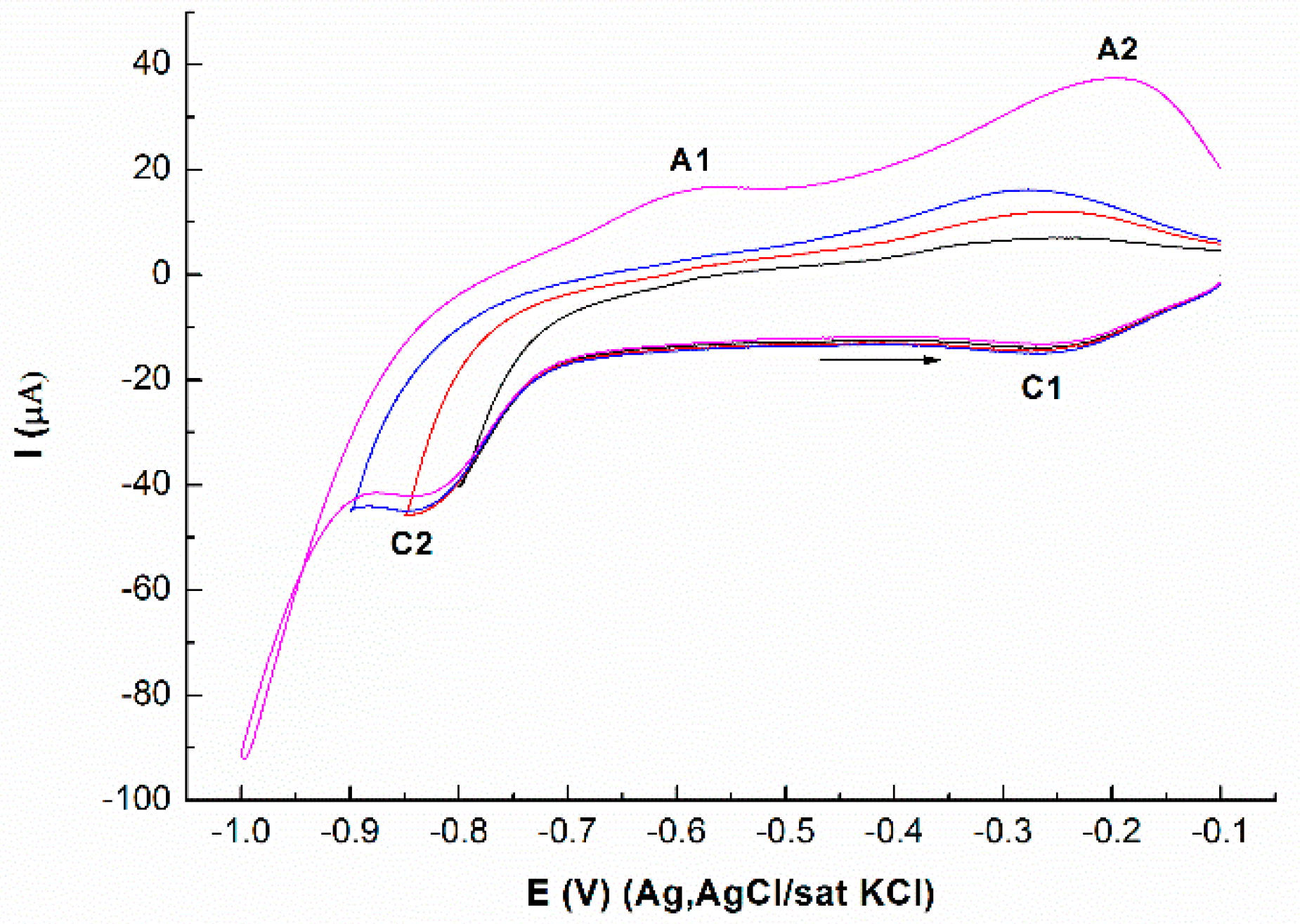
3.1. Deposition of Mo Atomic Layers on Ag(111)

The deposition of Mo from (NH4)6Mo7O24·4H2O 1 mM was performed in a pH 9.2 ammonia buffer. The predominant species in the working solution (pH 9.2 and a concentration of molybdenum of 7 mM) is the monomeric ion MoO42−. The MoO42− in aqueous solutions reaches the equilibrium quickly with the polymeric molybdate species [Mo7O24]6−. At pH below 6, polymerisation of MoO42− occurs through linking of MoO6 octahedra, yielding the heptamolybdate ion [Mo7O24]6− (pH 5–6) and the octamolybdate ion [Mo8O26]4− (pH 3–5). [49]. Figure 1 shows the voltammograms of the solution 7 mM MoO42− in a pH 9.2 ammonia buffer solution on Ag(111). The increase in the cathodic current at −0.26 V (C1) is not yet completely clear and has the shape of a very wide peak. Setting the potential end of the cyclic voltammogram to a more negative value, first a reduction peak appears at −0.8 V, and at −0.9 V, a second reduction process occurs. The peak at −0.8 V (C2) is very close to the bulk reduction potential, which overlaps partially. According to the literature [45], these peaks correspond to MoO42− reduction to Mo(0), however, we cannot exclude that during the deposition there was no formation of a MoOx species.
The anodic scan shows two peaks at −0.56 V (A1) and −0.19 V (A2), which are probably related to the oxidation of Mo to MoO2, and in a conversion of the insoluble MoO2 to soluble MoO42, respectively.
Further analysis was performed to understand the reduction processes better.
Figure 2 shows the anodic stripping curves of Mo at different deposition potentials from −0.60 to −0.85 V, at a constant accumulation time of 15 min.
As elsewhere discussed [7,17,33,50], a way to reveal the surface limited character of an electrodeposition process is to study the charges measured in the previous anodic stripping as a function of the deposition potential and deposition time as shown in Figure 2b and Figure 3b. Figure 2b shows the stripping charges of the deposit obtained at different potential values, while the concentration and deposition time were kept constant. The charge (Q) versus potential curve exhibits a plateau from −0.74 and −0.76 V (Figure 2b). This range corresponds to the optimum potentials for the SLR.
In Figure 3, the charges measured in the previous anodic stripping of the deposited Mo are reported as a function of the accumulation time, at constant concentration and deposition potential (−0.75 V). The asymptotic trend was expected as we have a process limited by the surface. Then, the Mo can be underpotentially deposited on Ag(111), applying a potential at −0.75 V for 15 min. This procedure is very critical because at potentials more negative than −0.76 V, the Mo bulk deposition started.

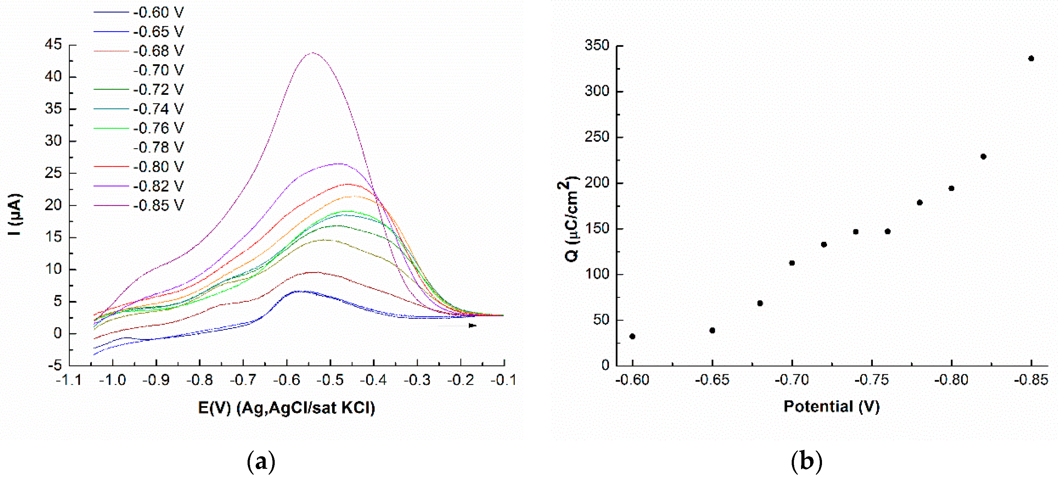
3.2. Deposition of Se on Atomic Layer of Mo on Ag(111)

The electrochemical characterization presented in the previous paragraph allowed the defining of a suitable set of parameters for the surface limited electrodeposition of an atomic monolayer of Mo on the Ag(111). The Mo ad-layer on Ag(111) (Moad/Ag(111)) can be deposited by applying a potential of −0.75 V for 15 minutes to the solution of 7 mM MoO42− in ammonia buffer pH 9.2. In the following, the deposition of Se on Moad/Ag(111) will be explained. Figure 4 reports the voltammograms of 1 mM SeO32− in a pH 9.2 ammonia buffer solution on Moad/Ag(111).
The voltammograms were registered at a more negative potential than the dissolution of Mo. The charge involved in the cathodic peak at −0.97 V reached a limiting value after five scans. In analogy, with what happens on Ag, this peak can be attributed to the bulk reduction of Se(0) to Se(-II) [51]; in our case, in the presence of Mo, this reaction was anticipated at about 30 mV. The positive current at −0.75 V indicates the reoxidation of Se(-II) to Se(0). Then, the procedure to obtain a layer of selenium consists in producing Se(-II) at −1.10 V, keeping constant the potential at −0.85 V for 5 min (to avoid reoxidation of Se(-II), to form Se(0) by comproportionation, and finally a washing step with the solution of the supporting electrolyte at −0.85 V for 1 min to reduce bulk selenium. Figure 5 shows cathodic stripping curves of the deposited Se as a function of the accumulation time, at a constant concentration and deposition potential.
The area of the peak at −1.14 V reached a constant value when performed after 5 min of accumulation time (−0.85 V for 5 min), with the area under the curve being 37.6 µC·cm−2.

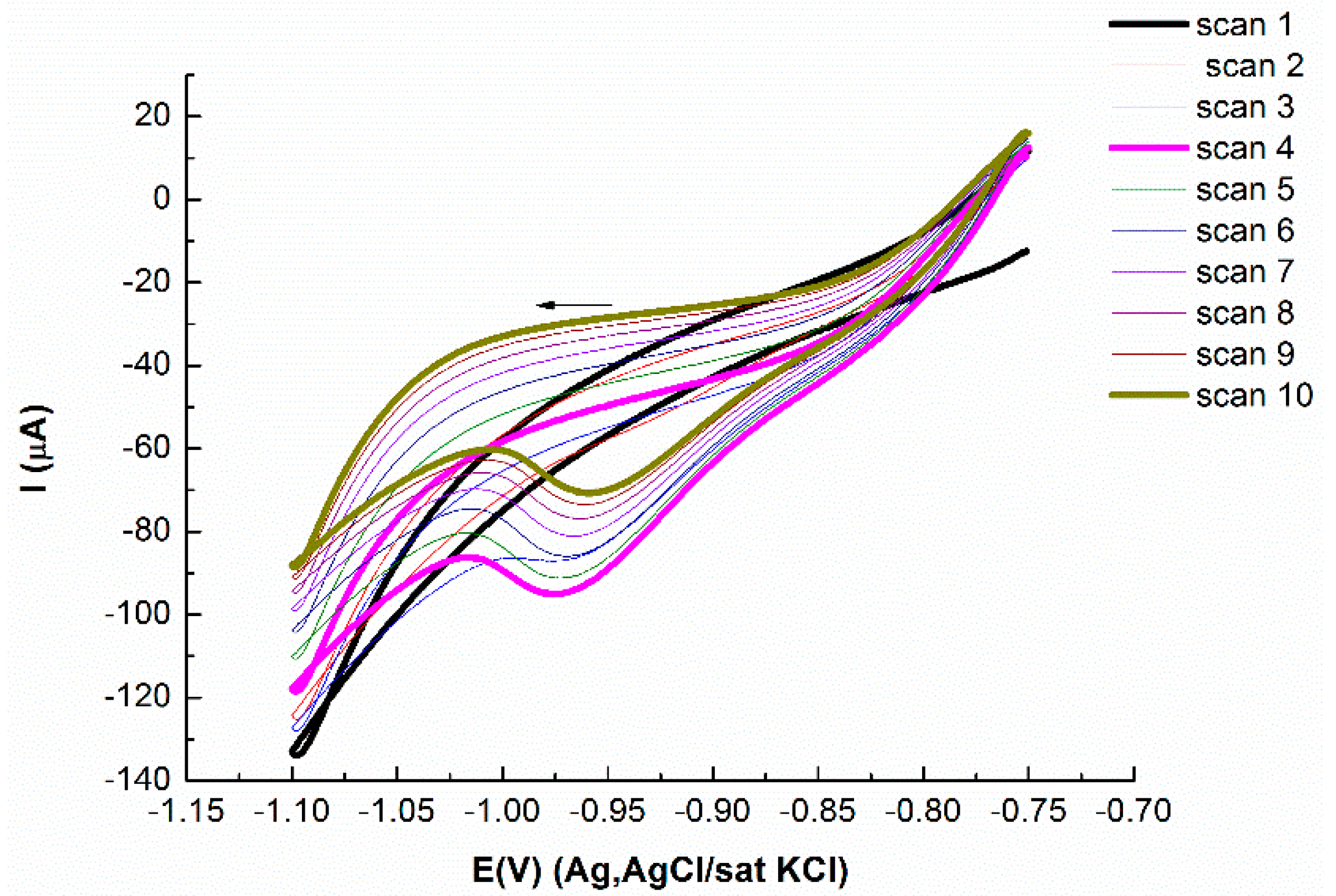
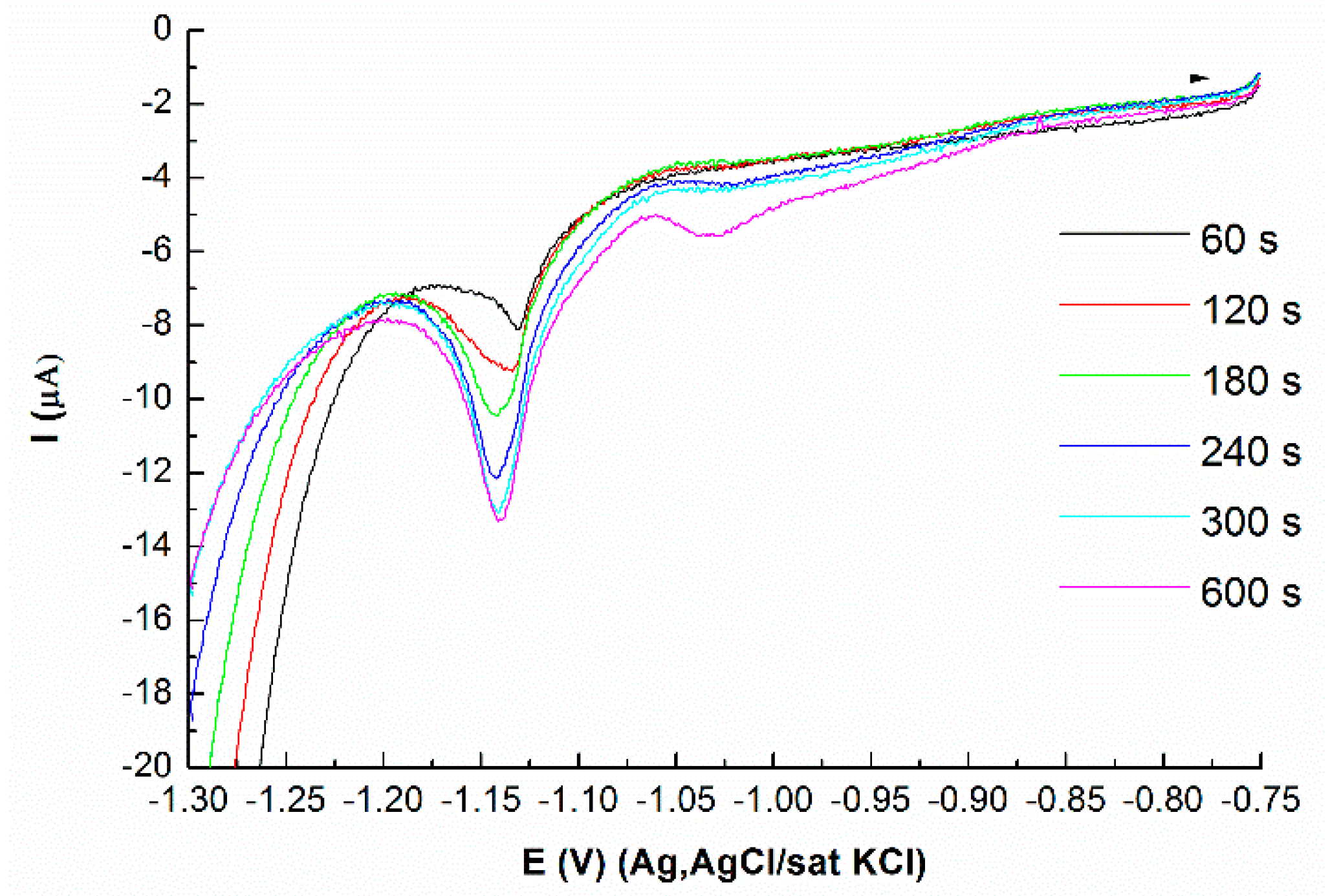
3.3. Deposition of Mo on Atomic Layer of Se on Ag(111)

To produce a 2D film of MoSe2 on Ag(111), we started the deposition with a Se ad-layer. The formation of the Se atomic layer on Ag(111) was described by Pezzatini et al. [22]. The Se ad-layer was deposited through a two-step procedure, from 1 mM SeO32− in a pH 9.2 ammonia buffer solution on Ag(111), by applying a potential of −0.90 V for 1 min, then 1 min at the same potential with the solution of the supporting electrolyte (washing step).
Figure 6 shows the voltammograms of the ammonia buffer pH 9.2 (black) and 7 mM MoO42− in ammonia buffer a pH 9.2 solution on Sead/Ag(111) (red and blue).
In the voltammograms of MoO42−, in the cathodic scanning, only the beginning of a reduction process is present, and compared to the CV on Ag(111), the peak at −0.8 V is absent. The absence of the peaks before the reduction process at −0.85 V proves that there are no surface limited electrochemical reactions. On this basis, we tried to deposit Mo at the beginning of the reduction process, e.g., at −0.85 V for 1 and 2 min, to verify if this is a bulk deposition (Figure 7).
The charges measured in the previous anodic stripping of the deposited Mo increased with the deposition time. Furthermore, the charge related to a 2 min-deposition was larger than that of Moad/Ag(111). Hence, the MoO42− reduction was hypothesized to be a bulk deposition, under the tested conditions.

4. Conclusions

The electrochemical behaviour of MoO42− on silver was investigated by cyclic voltammetry and anodic stripping voltammetry, finding results consistent with the study reported by Tsang et al. on Au(111) [45]. From the analysis of the deposited charges as a function of the accumulation potential and time, we found that Moad on Ag(111) can be deposited by applying a potential of −0.75 V for 15 min to a solution of MoO42−. The formation of the Moad on Ag(111) seems a particularly slow process; indeed, the requested accumulation time is high. This may occur because the deposition of Mo on Ag(111) involves the exchange of seven electrons with the metal substrate. Therefore, this process does not seem to be kinetically favoured. Both the absence of metals other than Mo and the surface limited character of the Moad allowed the exclusion of induced codeposition as a mechanism for the growth of the latter [52]. The parameters of electrodeposition of Se on Moad/Ag(111) were also investigated, finding the conditions for the growth of the Se ad-layer on Moad/Ag(111). The constant peak area of the cathodic stripping voltammetry of Se on Moad/Ag(111) after 5 minutes of accumulation time suggests the formation of an ad-layer of Se UPD on Moad/Ag(111). However, the deposition of Se on Moad/Ag(111) requires a higher accumulation time than the one of Se UPD on Ag(111), suggesting that the formation of a Sead/Moad/Ag(111) is less kinetically favoured than the one of Sead/Ag(111). In order to produce a 2D film of MoSe2 on Ag(111), the electrochemical behaviour of Mo on Sead/Ag(111) was investigated. The results show that only a bulk deposition of Mo on Sead/Ag(111) can be obtained in the investigated conditions.
In conclusion, the E-ALD method was used to produce a 2D thin film of Sead/Moad/Ag(111), which can potentially be applied in various technological applications, especially in the optoelectronic field [39]. Further investigations are needed to develop the conditions for extending the E-ALD method to the growth of thin MoSe2 films.

Author Contributions

Conceptualization, A.G. and M.I.; methodology, A.G., A.L. and E.P.; investigation, M.V., E.S., R.A.P., A.D.L. and L.F.; writing—original draft preparation M.V., A.G.; writing—review and editing, A.G, E.S., F.G., W.G., M.P., N.C., R.A.P. and M.I.

Acknowledgments

The authors acknowledge the financial support that has been given from Regione Toscana POR CreO FESR 2014-2020—azione 1.1.5 sub-azione a1 Bando 2 “Progetti di ricerca e sviluppo delle MPMI” which made possible the project “Gioielli in Argento Da Galvanica Ecologica e Tecnologica” (GADGET), “Tecnologia al plasma per l’industria del lusso: una manifattura innovativa nel comparto accessori in ottica 4.0” (THIN FASHION).

Conflicts of Interest

The authors declare no conflict of interest.

References

  1. Fabricating Energy Devices with Low Environmental Impacts. Available online: http://www.spie.org/newsroom/6249-fabricating-energy-devices-with-low-environmental-impacts?SSO=1 (accessed on 11 January 2016).
  2. Lu, W.; Lieber, C.M. Nanoelectronics from the bottom up. Nat. Mater. 2007, 6, 841–850. [Google Scholar] [CrossRef] [PubMed] [Green Version]
  3. Stickney, B.W.; Gregory, J.L. Electrochemical atomic layer epitaxy (ECALE). J. Electroanal. Chem. 1991, 300, 543–561. [Google Scholar]
  4. Lay, M.D.; Varazo, K.; Stickney, J.L. Formation of Sulfur Atomic Layers on Gold from Aqueous Solutions of Sulfide and Thiosulfate: Studies Using EC-STM, UHV-EC, and TLEC. Langmuir 2003, 19, 8416–8427. [Google Scholar] [CrossRef]
  5. Cavallini, M.; Aloisi, G.; Guidelli, R. In situ STM study of selenium electrodeposition on Ag(111). Langmuir 1999, 15, 2993–2995. [Google Scholar] [CrossRef]
  6. Aloisi, G.D.; Cavallini, M.; Innocenti, M.; Foresti, M.L.; Pezzatini, G.; Guidelli, R. In situ STM and electrochemical investigation of sulfur oxidative underpotential deposition on Ag(111). J. Phys. Chem. B 1997, 101, 4774–4780. [Google Scholar] [CrossRef]
  7. Innocenti, M.; Bencista, I.; Di Benedetto, F.; Cinotti, S.; De Luca, A.; Bellandi, S.; Lavacchi, A.; Muniz Miranda, M.; Vizza, F.; Marinelli, F.; et al. Underpotential Deposition of Sn on S-Covered Ag(111). ECS Trans. 2013, 50, 1–7. [Google Scholar] [CrossRef]
  8. Oviedo, O.A.; Reinaudi, L.; Garciía, S.G.; Leiva, E.P.M. Underpotential Deposition: From Fundamentals and Theory to Applications at the Nanoscale; Springer: Berlin, Germany, 2016; ISBN 9783319243948. [Google Scholar]
  9. Giaccherini, A.; Felici, R.; Innocenti, M. Operando structural characterization of the E-ALD process ultra-thin films growth. In X-ray Characterization of Nanostructured Energy Materials by Synchrotron Radiation; IntechOpen: Rijeka, Croatia, 2017. [Google Scholar]
  10. Salvietti, E.; Giaccherini, A.; Gambinossi, F.; Foresti, M.L.; Passaponti, M.; Di Benedetto, F.; Innocenti, M. E-ALD: Tailoring the Optoeletronic Properties of Metal Chalcogenides on Ag Single Crystals. Semicond. Growth Charact. 2018. [Google Scholar] [CrossRef] [Green Version]
  11. Di Benedetto, F.; Bencistà, I.; Caporali, S.; Cinotti, S.; De Luca, A.; Lavacchi, A.; Vizza, F.; Muniz Miranda, M.; Foresti, M.L.; Innocenti, M. Electrodeposition of ternary CuxSnySz thin films for photovoltaic applications. Prog. Photovolt. Res. Appl. 2014, 22, 97–106. [Google Scholar] [CrossRef]
  12. Bencistà, I.; Di Benedetto, F.; Innocenti, M.; De Luca, A.; Fornaciai, G.; Lavacchi, A.; Montegrossi, G.; Oberhauser, W.; Pardi, L.A.; Romanelli, M.; et al. Phase composition of CuxS thin films: Spectroscopic evidence of covellite formation. Eur. J. Mineral. 2012, 24, 879–884. [Google Scholar] [CrossRef]
  13. Lastraioli, E.; Loglio, F.; Cavallini, M.; Simeone, F.C.; Innocenti, M.; Carlaà, F.; Foresti, M.L. In Situ Scanning Tunneling Microscopy Investigation of Sulfur Oxidative Underpotential Deposition on Ag(100) and Ag(110). Langmuir 2010, 26, 17679–17685. [Google Scholar] [CrossRef]
  14. Innocenti, M.; Bencistà, I.; Bellandi, S.; Bianchini, C.; Di Benedetto, F.; Lavacchi, A.; Vizza, F.; Foresti, M.L. Electrochemical layer by layer growth and characterization of copper sulfur thin films on Ag(111). Electrochim. Acta 2011, 58, 599–605. [Google Scholar] [CrossRef]
  15. Innocenti, M.; Bellandi, S.; Lastraioli, E.; Loglio, F.; Foresti, M.L. Selective electrodesorption based atomic layer deposition (SEBALD): A novel electrochemical route to deposit metal clusters on Ag(111). Langmuir 2011, 27, 11704–11709. [Google Scholar] [CrossRef] [PubMed]
  16. Innocenti, M.; Cattarin, S.; Cavallini, M.; Loglio, F.; Foresti, M.L. Characterisation of thin films of CdS deposited on Ag(111) by ECALE. A morphological and photoelectrochemical investigation. J. Electroanal. Chem. 2002, 532, 219–225. [Google Scholar] [CrossRef]
  17. Innocenti, M.; Becucci, L.; Bencistà, I.; Carretti, E.; Cinotti, S.; Dei, L.; Di Benedetto, F.; Lavacchi, A.; Marinelli, F.; Salvietti, E.; et al. Electrochemical growth of Cu-Zn sulfides. J. Electroanal. Chem. 2013, 710, 17–21. [Google Scholar] [CrossRef]
  18. Di Benedetto, F.; Cinotti, S.; Guerri, A.; De Luca, A.; Lavacchi, A.; Montegrossi, G.; Carlà, F.; Felici, R.; Innocenti, M. Physical Characterization of Thin Films of CuxZnySz For Photovoltaic Applications. ECS Trans. 2013, 58, 59–65. [Google Scholar] [CrossRef]
  19. Giaccherini, A.; Russo, F.; Carlà, F.; Guerri, A.; Picca, R.A.; Cioffi, N.; Cinotti, S.; Montegrossi, G.; Passaponti, M.; Di Benedetto, F.; et al. Operando SXRD of E-ALD deposited sulphides ultra-thin films: Crystallite strain and size. Appl. Surf. Sci. 2018, 432, 53–59. [Google Scholar] [CrossRef] [Green Version]
  20. Giaccherini, A.; Montegrossi, G.; Di Benedetto, F.; Innocenti, M. Thermochemistry of the E-ALD process for the growth of CuxZnyS on Ag(111): Interpretation of experimental data. Electrochim. Acta 2018, 262. [Google Scholar] [CrossRef]
  21. Berretti, E.; Cinotti, S.; Caporali, S.; Cioffi, N.; Giaccherini, A.; Di Benedetto, F.; Foresti, M.L.; Montegrossi, G.; Lavacchi, A.; Vizza, F.; et al. Electrodeposition and Characterization of p and n Sulfide Semiconductors Composite Thin Film. J. Electrochem. Soc. 2016, 163, D3034–D3039. [Google Scholar] [CrossRef]
  22. Pezzatini, G.; Caporali, S.; Innocenti, M.; Foresti, M.L. Formation of ZnSe on Ag(111) by electrochemical atomic layer epitaxy. J. Electroanal. Chem. 1999, 475, 164–170. [Google Scholar] [CrossRef]
  23. Foresti, M.L.; Milani, S.; Loglio, F.; Innocenti, M.; Pezzatini, G.; Cattarin, S. Ternary CdSxSe1−x deposited on Ag(111) by ECALE: Synthesis and characterization. Langmuir 2005, 21, 6900–6907. [Google Scholar] [CrossRef] [PubMed]
  24. Gregory, B.W.; Norton, M.L.; Stickney, J.L. Thin-layer electrochemical studies of the underpotential deposition of cadmium and tellurium on polycrystalline Au, Pt and Cu electrodes. J. Electroanal. Chem. 1990, 293, 85–101. [Google Scholar] [CrossRef]
  25. Loglio, F.; Innocenti, M.; Jarek, A.; Caporali, S.; Pasquini, I.; Foresti, M.L. Nickel sulfur thin films deposited by ECALE: Electrochemical, XPS and AFM characterization. J. Electroanal. Chem. 2010, 638, 15–20. [Google Scholar] [CrossRef]
  26. Russo, F.; Giaccherini, A.; Salvietti, E.; Berretti, E.; Passaponti, M.; Lavacchi, A.; Montegrossi, G.; Piciollo, E.; Di Benedetto, F.; Innocenti, M. Morphology and composition of Cu2S ultra-thin films deposited by E-ALD. ECS Trans. 2017, 80, 749–756. [Google Scholar] [CrossRef]
  27. Innocenti, M.; Cinotti, S.; Bencista, I.; Carretti, E.; Becucci, L.; Di Benedetto, F.; Lavacchi, A.; Foresti, M.L. Electrochemical Growth of Cu-Zn Sulfides of Various Stoichiometries. ECS Trans. 2014, 161, D14–D17. [Google Scholar] [CrossRef]
  28. Caporali, S.; Tolstogouzov, A.; Teodoro, O.M.N.D.N.D.; Innocenti, M.; Di Benedetto, F.; Cinotti, S.; Picca, R.A.; Sportelli, M.C.; Cioffi, N. Sn-deficiency in the electrodeposited ternary CuxSnySz thin films by ECALE. Sol. Energy Mater. Sol. Cells 2015, 138, 9–16. [Google Scholar] [CrossRef]
  29. Cecconi, T.; Atrei, A.; Bardi, U.; Forni, F.; Innocenti, M.; Loglio, F.; Foresti, M.L.; Rovida, G. X-ray photoelectron diffraction (XPD) study of the atomic structure of the ultrathin CdS phase deposited on Ag(111) by electrochemical atomic layer epitaxy (ECALE). J. Electron Spectrosc. Relat. Phenom. 2001, 114–116, 563–568. [Google Scholar] [CrossRef]
  30. Loglio, F.; Innocenti, M.; D’Acapito, F.; Felici, R.; Pezzatini, G.; Salvietti, E.; Foresti, M.L. Cadmium selenide electrodeposited by ECALE: Electrochemical characterization and preliminary results by EXAFS. J. Electroanal. Chem. 2005, 575, 161–167. [Google Scholar] [CrossRef]
  31. Cavallini, M.; Facchini, M.; Albonetti, C.; Biscarini, F.; Innocenti, M.; Loglio, F.; Salvietti, E.; Pezzatini, G.; Foresti, M.L. Two-Dimensional Self-Organization of CdS Ultra Thin Films by Confined Electrochemical Atomic Layer Epitaxy Growth. J. Phys. Chem. C 2007, 111, 1061–1064. [Google Scholar] [CrossRef]
  32. Huang, B.M.; Colletti, L.P.; Gregory, B.W.; Anderson, J.L.; Stickney, J.L. Preliminary studies of the use of an automated flow-cell electrodeposition system for the formation of CdTe thin films by electrochemical atomic layer epitaxy. J. Electrochem. Soc. 1995, 142, 3007–3016. [Google Scholar] [CrossRef]
  33. Innocenti, M.; Pezzatini, G.; Forni, F.; Foresti, M.L.F. CdS and ZnS Deposition on Ag(111) by Electrochemical Atomic Layer Epitaxy. J. Electrochem. Soc. 2001, 148, C357–C362. [Google Scholar] [CrossRef]
  34. Keyshar, K.; Berg, M.; Zhang, X.; Vajtai, R.; Gupta, G.; Chan, C.K.; Beechem, T.E.; Ajayan, P.M.; Mohite, A.D.; Ohta, T. Experimental Determination of the Ionization Energies of MoSe2, WS2, and MoS2 on SiO2 Using Photoemission Electron Microscopy. ACS Nano 2017, 11, 8223–8230. [Google Scholar] [CrossRef] [PubMed]
  35. Wang, Y.; Zhang, F.; Wang, Q.; Yang, P.; Lin, H.; Qu, F. Hierarchical MoSe2 nanoflowers as novel nanocarriers for NIR-light-mediated synergistic photo-thermal/dynamic and chemo-therapy. Nanoscale 2018, 10, 14534–14545. [Google Scholar] [CrossRef] [PubMed]
  36. Wilcoxon, J.P.; Samara, G.A. Strong quantum-size effects in a layered semiconductor: MoS2 nanoclusters. Phys. Rev. B 1995, 51, 7299–7302. [Google Scholar] [CrossRef]
  37. Yuan, R.-Y.; Yang, Q.-J.; Guo, Y. Enhanced spin polarization and valley polarization in monolayer MoS2 junctions. J. Phys. Condens. Matter 2018, 30. [Google Scholar] [CrossRef] [PubMed]
  38. Lu, H.-Z.; Yao, W.; Xiao, D.; Shen, S.-Q. Intervalley Scattering and Localization Behaviors of Spin-Valley Coupled Dirac Fermions. Phys. Rev. Lett. 2013, 110, 016806. [Google Scholar] [CrossRef] [PubMed]
  39. Schaibley, J.R.; Yu, H.; Clark, G.; Rivera, P.; Ross, J.S.; Seyler, K.L.; Yao, W.; Xu, X. Valleytronics in 2D materials. Nat. Rev. Mater. 2016, 1, 16055. [Google Scholar] [CrossRef]
  40. Mueed, M.A.; Hossain, M.S.; Jo, I.; Pfeiffer, L.N.; West, K.W.; Baldwin, K.W.; Shayegan, M. Realization of a Valley Superlattice. Phys. Rev. Lett. 2018, 121, 036802. [Google Scholar] [CrossRef]
  41. Mak, K.F.; Xiao, D.; Shan, J. Light–valley interactions in 2D semiconductors. Nat. Photonics 2018, 12, 451–460. [Google Scholar] [CrossRef]
  42. Wang, X.; Gong, Y.; Shi, G.; Chow, W.L.; Keyshar, K.; Ye, G.; Vajtai, R.; Lou, J.; Liu, Z.; Ringe, E.; et al. Chemical Vapor Deposition Growth of Crystalline Monolayer MoSe2. ACS Nano 2014, 8, 5125–5131. [Google Scholar] [CrossRef]
  43. Boscher, N.D.; Carmalt, C.J.; Palgrave, R.G.; Gil-Tomas, J.J.; Parkin, I.P. Atmospheric Pressure CVD of Molybdenum Diselenide Films on Glass. Chem. Vap. Depos. 2006, 12, 692–698. [Google Scholar] [CrossRef]
  44. Chang, Y.-H.; Zhang, W.; Zhu, Y.; Han, Y.; Pu, J.; Chang, J.-K.; Hsu, W.-T.; Huang, J.-K.; Hsu, C.-L.; Chiu, M.-H.; et al. Monolayer MoSe2 Grown by Chemical Vapor Deposition for Fast Photodetection. ACS Nano 2014, 8, 8582–8590. [Google Scholar] [CrossRef] [PubMed]
  45. Tsang, C.F.; Ledina, M.A.; Stickney, J.L. Molybdenum diselenide formation using electrochemical atomic layer deposition (E-ALD). J. Electroanal. Chem. 2017, 793, 242–249. [Google Scholar] [CrossRef]
  46. Hamelin, A. Modern Aspects of Electrochemistry; Conway, B.E., White, R.E., Bockris, J.O., Eds.; Plenum Press: New York, NY, USA, 1985; Volume 16, pp. 1–101. [Google Scholar]
  47. Foresti, M.L.; Capolupo, F.; Innocenti, M.; Loglio, F. Visual Detection of Crystallographic Orientations of Face-Centered Cubic Single Crystals. Cryst. Growth Des. 2002, 2, 73–77. [Google Scholar] [CrossRef]
  48. Hamelin, A.; Stoicoviciu, L.; Doubova, L.; Trasatti, S. Influence of the crystallographic orientation of the surface on the potential of zero charge of silver electrodes. Surf. Sci. 1988, 201, L498–L506. [Google Scholar] [CrossRef]
  49. Aveston, J.; Anacker, E.W.; Johnson, J.S. Hydrolysis of Molybdenum (VI). Ultracentrifugation, Acidity Measurements, and Raman Spectra of Polymolybdates. Inorg. Chem. 1964, 3, 735–746. [Google Scholar] [CrossRef]
  50. Foresti, M.; Pezzatini, G.; Cavallini, M.; Aloisi, G.; Innocenti, M.; Guidelli, R. Electrochemical atomic layer epitaxy deposition of CdS on Ag (111): An electrochemical and STM investigation. J. Phys. Chem. B 1998, 102, 7413–7420. [Google Scholar] [CrossRef]
  51. Pezzatini, G.; Loglio, F.; Innocenti, M.; Foresti, M.L. Selenium (IV) Electrochemistry on Silver: A Combined Electrochemical Quartz-Crystal Microbalance and Cyclic Voltammetric Investigation. Collect. Czechoslov. Chem. Commun. 2003, 68, 1579–1595. [Google Scholar] [CrossRef]
  52. Morley, T.J.; Penner, L.; Schaffer, P.; Ruth, T.J.; Bénard, F.; Asselin, E. The deposition of smooth metallic molybdenum from aqueous electrolytes containing molybdate ions. Electrochem. Commun. 2012, 15, 78–80. [Google Scholar] [CrossRef]
Figure 1. Cyclic voltammograms of 7 mM MoO42− on Ag(111) in a pH 9.2 ammonia buffer solution, different end scan. The scan rate is 50 mV·s−1.
Metals 09 00122 g001
Figure 2. (a) Anodic stripping curves after potentiostatic deposition of Mo at different potentials (deposition time 15 min) on Ag(111) in NaOH 0.1 M. The scan rate is 50 mV·s−1. (b) Plot of the charge density (Q) involved in the stripping of Mo deposited on Ag(111) as a function of the deposition potential, at a constant deposition time of 15 min.
Metals 09 00122 g002
Figure 3. (a) Anodic stripping curves of Mo deposited at E = −0.75 V on Ag (111) in NaOH 0.1 M. The scan rate is 50 mV·s−1. The curves refer to deposition times from 30 s to 15 min (b) Plot of the charges, Q, involved in the stripping of Mo deposited on Ag(111), as a function of the accumulation time, at a constant deposition potential of −0.75 V.
Metals 09 00122 g003
Figure 4. Consecutive cyclic voltammograms of 1 mM SeO32− on Moad/Ag(111) in a pH 9.2 ammonia buffer solution, different end scan. The scan rate is 50 mV·s−1.
Metals 09 00122 g004
Figure 5. Cathodic stripping curves of Se deposited at E = −0.85 V on Moad/Ag(111) in NaOH 0.1M. The scan rate is 10 mV·s−1. The curves refer to deposition times from 1 to 10 min.
Metals 09 00122 g005
Figure 6. Consecutive cyclic voltammograms of pH 9.2 ammonia buffer solution (black curves) and 7 mM MoO42− in a pH 9.2 ammonia buffer solution (red and blue curves, respectively) on Sead/Ag(111). The scan rate is 50 mV·s−1.
Metals 09 00122 g006
Figure 7. Anodic stripping curves of Mo deposited at E = −0.85 V on Sead/Ag(111) in ammonia buffer pH 9.2 after a −0.45 V washing step. The scan rate is 10 mV·s−1. The curves refer to deposition times from 1 and 2 min.
Metals 09 00122 g007

