1. Introduction
The growth of Internet services, such as streaming video, social networking, and cloud computing has created the fast-growing need for datacenters. Due to their low power consumption [
1], high modulation speed [
2], and low cost [
3], vertical-cavity surface-emitting lasers (VCSELs) based links dominate modern datacenter systems. A lot of development works have been carried out in the fabrication of VCSELs [
4,
5,
6]. For these diverse design structures, the number of quantum wells differs. As the demand for greater capacity increases, the VCSEL has incorporated equalization circuitry, embedded in drivers through CMOS technology [
7,
8]. To facilitate VCSEL design, fabrication and evaluation, an accurate VCSEL model, accommodating the variable quantum well (QW) number, needs to be built in an electronic-photonic co-simulation platform.
Previous models were proposed to simulate the performance of multi-quantum-well (MQW) VCSELs [
9,
10,
11]. In these models, the number of rate equations are proportional to the number of QWs such that the model cannot be generalized to all VCSEL designs [
12,
13], and are not suitable for the system-level simulation of VCSEL-based fiber links. The parameter extraction will also be a significant challenge in view of the extremely large number of parameters. In addition, these models do not account for noise effects, which are significant for assessing the transmission performance.
In this paper, we propose a versatile compact equivalent circuit model with noise effects for the MQW VCSEL. The proposed model accommodates a flexible number of quantum wells (QW’s), which provides the freedom to simulate an arbitrary VCSEL in the system-oriented opto-electronic simulation platform. The model is developed in the commercial Cadence tool suite, a schematic-driven tool for CMOS electronic integrated circuit design. The paper outline is as follows.
Section 2 explains the VCSEL parasitic circuit model, which determines the small-signal response. In
Section 3, the carrier and photon dynamisms are analyzed for the structure including separate confinement hetero-structure layers, barrier layers, and quantum well layers. In the QW layer, the carriers have two states: the confined state inside the quantum well and the unconfined state above the quantum well. In
Section 4, based on the VCSEL structure analysis, we obtain a set of rate equations for the MQW VCSEL. After that, a versatile compact rate equation set is obtained, with a significant reduction in the number of equations. Laser intensity noise is expressed based on the Markovian assumption and added to the compact rate equations. In
Section 5, the rate equations with noise terms are translated into the corresponding equivalent circuit equations. The equivalent circuit model for the MQW VCSEL is realized. In
Section 6, the accuracy of the proposed VCSEL model is validated using a self-wire-bonded 850 nm VCSEL. In
Section 7, we present a summary and then, conclude.
2. VCSEL Structure and Dynamism Analysis
Although designs and materials, used for the VCSELs, are not totally the same, these VCSELs have one typical common structure, as shown in
Figure 1a. Two multi-layered Bragg reflectors are located at the top of the p-doped region and at the bottom of the n-doped region, with the high-index layer and low-index layer alternating. Constructive interference is caused by the reflections at the interface between the high-index and low-index layers for the reflective wave around the Bragg wavelength, and the multiple layers act as a mirror to improve optical gain [
14]. The oxide layer, with a specific aperture size, transversely confines carriers to the active region. The p-doped and n-doped regions provide carrier injection for the active region between them.
The active region consists of separate confinement heterostructure (SCH) layers, barrier (B) layers, and quantum well (QW) layers, detailed in
Figure 1b. The SCH1 layer is adjacent to the n-doped region, while the SCH2 layer is adjacent to the p-doped region. The barrier layers are sandwiched between two adjacent QW layers and have a larger energy bandgap than the QWs. Conventionally, the QWs of 850 nm VCSELs are fabricated using GaAs. However, InGaAs QWs increase the differential gain, which is advantageous to reach higher speeds [
15]. In QW layers, carriers have two states: an unconfined state and a confined state. The confined state indicates the carriers are confined at the bottom of the wells and no longer free to move in three dimensions. The carriers in the unconfined state (also referred as the gateway (G) state) are free to move in three dimensions and occupy energy higher than the carriers in the confined state at the bottom of the well [
16]. Therefore, the gateway state can be viewed as an intermediate state for carriers originating from either a SCH or barrier layer. The MQW-SCH-G-B structure is widely adopted for 850 nm VCSEL devices [
12,
13]. In [
12], the VCSEL performance investigation uses a 7-nm-thick GaAs MQWs separated by 8-nm-thick Al
0.3Ga
0.7As barriers.
The dynamic behavior of the VCSEL is determined by the carrier and photon dynamism illustrated in
Figure 1c. The carriers are injected into the active region due to the injection current. Then, carriers drift with applied electric field between the top and bottom contacts (
Figure 1a) and diffuse from carrier concentration gradient between the n-doped and p-doped regions. Carrier movements between the two energy bands are labelled
capture when the carrier moves to a lower bandgap region, and
escape when it jumps to a higher bandgap region. Tunneling is the quantum process, where a carrier penetrates through a barrier region, facilitating a carrier motion between adjacent QW regions. Photons are generated via stimulated emission involving an electron-hole recombination.
3. Parasitic Circuit
A complete VCSEL model includes the extrinsic parasitic circuit description and the intrinsic rate-equation-based model. The parasitic circuit originates from the cavity structure explained in
Section 2 and determines the small-signal response. The rate-equation-based model reflects the variation in the number of carriers and photons inside the active region.
The complete parasitic circuit model is shown in
Figure 2a. The contact pads introduce resistance, capacitance and inductance to the parasitic circuit. Cp is the capacitance between the contacts, the resistance Rp represents the contact pad loss, and Lp is the inductance induced by the contacts. The resistance Rt and Rb model the top, and bottom Bragg reflectors, respectively. The oxide layer capacitance, Cox, is in series with the junction capacitance, Cj. The resistance of the active region, Ra, is parallel with the series connection of Cox and Cj. The time-varying current flowing through Ra serves as the input to the rate equation model. In
Figure 2b, we simplify the parasitic circuit for further circuit analysis and modeling. The series connection of Cox and Cj leads to Ca, and the combination of the top and bottom Bragg reflector resistances leads to Rm.
Based on
Figure 2b, the input impedance of the parasitic circuit is expressed as,
where
f is the frequency of the modulation signal and
j is the imaginary unit.
The active region injection current with respect to time
t,
Ia(
t), is expressed in Equation (2),
where
Id is the amplitude of the time-varying high-speed driving current.
Due to Joule ohmic heating and free carrier absorption loss, the VCSEL self-heating effect leads to temperature elevation of the laser cavity [
17]. The parasitic elements in the active region,
Rm,
Ra and
Ca, are modelled as the function of the active region temperature, as shown in Equation (3),
where
a0,
a1,
a2,
a3 and
a4 are the polynomial coefficients,
T is the VCSEL cavity temperature in Kelvin, and
T0 is the relative temperature subtracted from
T to reduce the requirement for coefficient extraction precision.
The active region temperature is expressed as follows due to the self-heating effect,
where
Tamb is the ambient temperature,
V is the device voltage,
I is the driving current,
P is the output light power,
Rth is the thermal impedance of the VCSEL, and
τth is the thermal time constant.
Considering the excellent thermal conductivity of the contact pads and relatively large gap between pads and the active region, it is accurate enough to regard Rp, Cp, and Lp as temperature-independent.
4. Compact Rate Equations
The SCH-QW-G-B bandgap structure in
Section 2 is modeled using the set of rate equations expressing the carrier and photon dynamisms. In this section, the rate equation model describes the intrinsic behaviors of a MQW VCSEL with more complete carrier and photon dynamisms than previously reported [
18,
19]. We first derive the rate equations for the two SCH layers (SCH
1 and SCH
2) of the active regions. Carriers injected into SCH
1 make their way to SCH
2. The carrier movement between a SCH layer and an unconfined state in an adjacent QW layer determines the carrier quantity. In addition, electron-hole recombination in the SCH layer with high carrier density is included. The variations in carrier numbers with respect to time in the two SCH regions are expressed by the differential equations below,
where
NSCH(i) and
RSCH(i) represent the carrier number and the combination rate in SCH
1 (
i = 1) and SCH
2 (
i = 2).
ηinj is the current injection efficiency (dimensionless) and
q is the electron charge. The injection current
Ia(t) is a time-varying high-speed signal, and
Ileak is the leakage current.
NG(j) is the unconfined carrier number in the gateway state of the QW layer, where the subscript
j denotes the gateway state in the
jth QW layer counting from the bottom of the active region (in
Figure 1b). The number of gateway states in the active region is the same as the number of QWs (denoted as
nw), therefore 1 ≤
j ≤
nw.
τD is the effective carrier transport time between a SCH or barrier layer and its adjacent gateway state.
Next, the gateway rate equations for the carriers are derived. In the first gateway state (at the bottom of the active region in
Figure 1b) and the last gateway state (at the top), the following effects are considered: the carrier exchange with the adjacent SCH or barrier layer, the electron-hole recombination, and the carrier exchange with the confined states within the QW layer. Equation (7) represents the rate equation for the unconfined carriers in the bottom QW layer (
j = 1),
where
NB(1) is the carrier number in the bottom barrier layer,
NW(1) and
RG(1) are the confined carrier number and the recombination rate of the unconfined carriers in the bottom QW layer, respectively.
τesc and
τcap are the QW carrier escape, and capture lifetimes, respectively. The rate equation for unconfined carriers in the top QW layer is expressed in (8),
where the subscript
nw represents the top layer. For gateway states in the other QW layers (i.e., 2 ≤
j ≤
nw-1) which are adjacent to two barrier layers, the rate equation is expressed by Equation (9):
Similarly, in the barrier layer, we consider the carrier exchange between the barrier layer and the two adjacent gateway states as well as the electron-hole recombination using Equation (10),
where
RB(k) is the recombination rate in the
kth barrier layer.
For confined carriers by the quantum wells, the dynamisms, such as carrier capture/escape, quantum tunneling, spontaneous and stimulated emissions, and recombination, are accounted. The following equation represents the rate equation for confined carriers in the first QW layer,
where
SW(1) represents the photon number in this QW layer.
τtun is the tunneling time, and
vg is the group velocity of the lasing medium.
RW(1),
ΓW(1) and
GW(1) represent the recombination rate, the optical confinement factor, and the gain coefficient for the confined carriers. The rate equation for the confined carriers in the last QW layer is expressed as the following,
where the subscript is replaced to represent the top layer (
nw). The rate equation for confined carriers in all other QW layers is expressed as follows, where the subscript is generalized to
j to represent the
jth QW layer:
Finally, Equation (14) accounts for the photon number generated in the
jth QW,
where
τp is the photon lifetime.
Rωβ(j) represents the rate of electron-hole recombination of the lasing mode.
The rate equations describing these carrier and photon dynamisms are detailed above. The number of differential rate equations reaches 4·
nw+1 for a VCSEL where
nw corresponds to the number of QWs, leading to a challenging computation complexity. In addition, parameter extraction from the experimental results is required to simulate and evaluate the performance of the manufactured VCSEL. The number of parameters included in the aforementioned equations is relatively large, which challenges parameter extraction. Furthermore, the proposed rate equations are strongly dependent on the number of QWs, such that the model cannot be generalized to all VCSEL designs as those in [
12,
13], where the numbers of QWs in these designs are quite different. It is, therefore, necessary to manipulate the rate Equations (5)–(14) to make them independent from the number of QWs. The detailed analysis of carrier and photon behaviors builds a set of rate equations for their comprehensive dynamisms, and the inclusion of the gateway states bridges SCH layers and QW layers. Consequently, the issues mentioned above are overcome by a series of transformations of rate equations.
Combining Equations (5) to (10), Equation (15) below describes the variation in the total number of unconfined carriers,
NS,
where
N is the total number of confined carriers inside each a QW. The total number of unconfined carriers,
NS, and of confined carriers,
N, in all layers are expressed as the following:
The total recombination rate for the unconfined carriers in all layers gives the equivalent recombination rate as,
RNS, which shows the total number of recombined unconfined carriers per unit time:
The equivalent escape lifetime
τe is equal to
τesc, while the equivalent capture lifetime
τc is expressed as the following:
The confined carrier dynamisms are expressed below by combining Equations (11) to (13),
where the photon number
S is the total number of photons in QW layers,
RN is the total recombination rate for the confined carriers, and
GN is the gain coefficient weighted by optical confinement factors. These can be expressed as the following:
For the photon dynamisms, Equation (21) is derived from the summation of (14) over the QW position
j:
With respect to Equations (15), (19) and (21), the equation set for the carrier and photon dynamisms consists of three differential equations, an important reduction in computation for the modeling of a laser source with MQWs. Assuming each differential equation consumes the same computation time, the calculation efficiency, defined as the reciprocal of the computation time for the whole equation set, improves by 3.3-fold for a laser source with three QWs and by 6-fold for five QWs.
The recombination rate terms
,
and
consist of three main types of recombination: Shockley-Read-Hall (SRH) non-radiative recombination, radiative recombination and Auger non-radiative recombination. A three-order polynomial based on the ABC model [
20] describes recombination terms, where
,
and
are SRH recombination coefficients for unconfined carriers, confined carriers and photons,
,
and
are corresponding radiative recombination coefficients, and
,
and
are corresponding Auger recombination coefficients. The expressions for
,
and
are expressed in Equation (22). Specifically, the radiative recombination dominates the photon generation, and non-radiative recombination effects are negligible. Therefore, values of
and
are set to 0.
The strong thermal dependence of VCSEL I–P characteristics is mainly attributed to the temperature-dependent carrier leakage out of the active region [
21]. The carrier leakage is represented by the leakage current
Ileak in Equation (15), which is expressed by a fourth-order polynomial of temperature in Equation (23). It is worth mentioning that the fourth-order polynomial provides sufficient parameter fitting accuracy and acceptable computation complexity,
where
b0,
b1,
b2,
b3, and
b4 are the polynomial coefficients. In the same way as Equation (3),
T0 is subtracted from
T to reduce the requirement for coefficient fitting precision.
The weighted gain coefficient
GN is expressed as follows [
22,
23]:
where
G0 is the gain coefficient,
ε is gain suppression factor, and
N0 is the transparency carrier density.
Laser noise is important in the VCSEL model. As such, the noise terms
FNS,
FN,
FS are added to the right-hand side of Equations (15), (19) and (21), accounting for fluctuation in
NS,
N and
S. The noise-inclusive rate-equations are expressed below as Equations (25) to (27):
Based on the Markovian assumption that the noise sources have relatively small correlation time compared to the carrier and photon lifetimes [
24,
25],
FNS,
FN and
FS satisfy the following correlation functions,
where the angle bracket represents time-average operator, and
δ(t) is the Kronecker delta function.
DK,J is the diffusion coefficient, described by Equation (29),
where
Rsp is the spontaneous emission rate, and
τn is the carrier recombination lifetime. With Equations (28) and (29),
FNS,
FN,
FS are mathematically expressed in Equation (30),
where
x1,
x2 and
x3 are independent Gaussian random variables with zero mean and unitary standard deviation.
5. VCSEL Equivalent Circuit Model
To realize the hybrid electronic-photonic modeling, the noise-inclusive rate Equations (25)–(27) are translated into a set of equations describing circuits. The equivalent circuit model is derived based on these circuit-described equations. To eliminate non-physical solutions of the carrier and photon dynamisms, Equation (31) is used to ensure that
NS and
N are positive values,
where
NSEQ and
NEQ are the densities of unconfined and confined carriers in thermal equilibrium at zero bias, and
Vact and
VQW are the volumes of the active region and the single QW.
VT,
V, and
Vw are the thermal voltage, and the voltages across the SCH and QW layers, respectively. The relationship between the total number of photons
S and the optical output power
Po is expressed as Equation (32),
where
λ is the free space wavelength,
τp is the photon lifetime,
ηc is the output power coupling coefficient,
ħ is reduced Planck constant, and
c is the light speed in free space. By substituting (31) into (25), Equation (33) is obtained to represent the equivalent circuit for the unconfined carriers in terms of current variables,
where
In addition, Equation (34) is derived by substituting (31) and (32) into (26), which represents the equivalent circuit for the confined carriers in QWs,
where
Substituting (32) into (27), Equation (35) is obtained, describing the equivalent circuit for the photon dynamism,
where:
The equivalent circuit schematic is shown in
Figure 3, based on Equations (33)–(35). The equivalent circuit model is realized in the Cadence Virtuoso environment based on the Verilog-A language. As seen from the mathematical derivations above,
IC,
ICω and
IL are considered as constant current sources, while
ID and
IDω are regarded as currents passing through a diode with the diode ideality factors equal to 2. Other current components,
IRS,
IR1,
IR2,
IS1,
IS2,
I1,
I2,
IFNS,
IFS and
IFN, are generated by time-varying current-controlled current sources. The circuit in the bottom right corner of
Figure 3 converts
VO to the practical optical power output,
PO.
RL is an arbitrary resistor for completeness of the closed circuit, and its value does not influence the functionality of the circuit model.
6. Results and Discussion
The model validation and parameter extraction are divided into two parts: One is for the parasitic circuit and the other is for the circuits of carrier and photon dynamisms. For parameter extraction of the parasitic circuit, the S11 data are utilized. For the circuits of carrier and photon dynamisms, the measurement results of output optical powers under different bias currents are utilized.
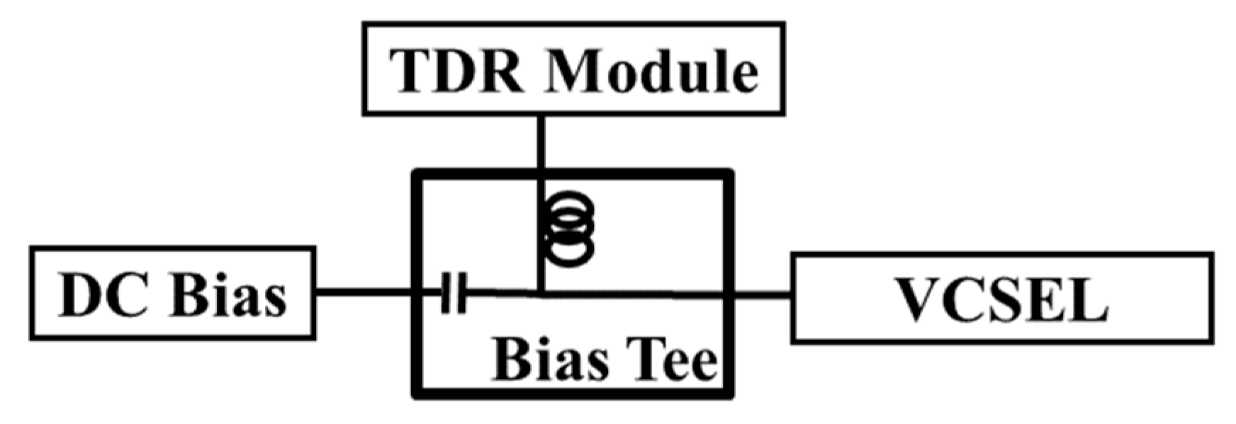
The experimental setup for S
11 measurement is shown in
Figure 4. A bias-tee is employed to combine the bias current and the small signal from a high-precision time-domain reflectometer (TDR). After the bias-tee, an 850 nm VCSEL chip is driven. S
11 data are measured by the TDR module. The self-wire-bonded VCSEL chip under test is manufactured by II-VI Incorporated.
The measurement for I-V-P data (I for injection current; V for VCSEL voltage; P for optical power) is performed automatically using the computer program, and the experimental schematic diagram for I-V-P measurement is shown in
Figure 5. The DC power supply is controlled by a personal computer (PC) to change the output voltage. A resistor of 462 Ω is used to protect the VCSEL, which voltage is recorded by a multi-meter. Therefore, the current passing through the resistor and the VCSEL can be obtained using Ohm’s law. The fiber couples the light of the VCSEL and is connected to an optical power meter. The optical power meter data is recorded by a PC. Based on the I-V-P data, the VCSEL temperatures under different bias currents are obtained using Equation (4) with
Rth = 2 × 10
3 K/W. It needs to be pointed out that the differential term in the right-hand side of Equation (4) is equal to zero for the steady state.
The expression for the magnitude of S
11 is shown below based on Equation (1),
where
Z0 = 50 Ω is the measurement system impedance.
The values of parasitic electrical elements are extracted using the least squares algorithm. The mean-square error between the calculated magnitude of S
11 by Equation (36) and the measured data is minimized to determine the optimal value of each element. The extracted values of Cp, Lp and Rp are given in
Table 1, and the polynomial coefficients of Rm, Ra and Ca are given in
Table 2. The measured data and the simulation curves of S
11 are depicted in
Figure 6a. The calculated S
11 can fit the measured data very well.
Curve fitting of large-signal DC responses is utilized to extract the parameters for the rate equations which describe the VCSEL electro-optical dynamisms. With the obtained VCSEL temperatures, the coefficients b0-b4 are extracted by minimizing the sum of the squares of the residuals between the simulation and measurement results of the leakage current.
T0 in Equation (23) is chosen as 300 K. Under steady states, rate equations are simplified into the non-differential nonlinear equations. The temperature-independent parameters of nonlinear equations are extracted by fitting the I-P curve.
Table 3 presents parameters of the rate equations, which are extracted by curve fitting. The simulated I-P curve and the experimental result are depicted in
Figure 6b, and they match with each other very well. Based on the extracted parameters in
Table 1,
Table 2 and
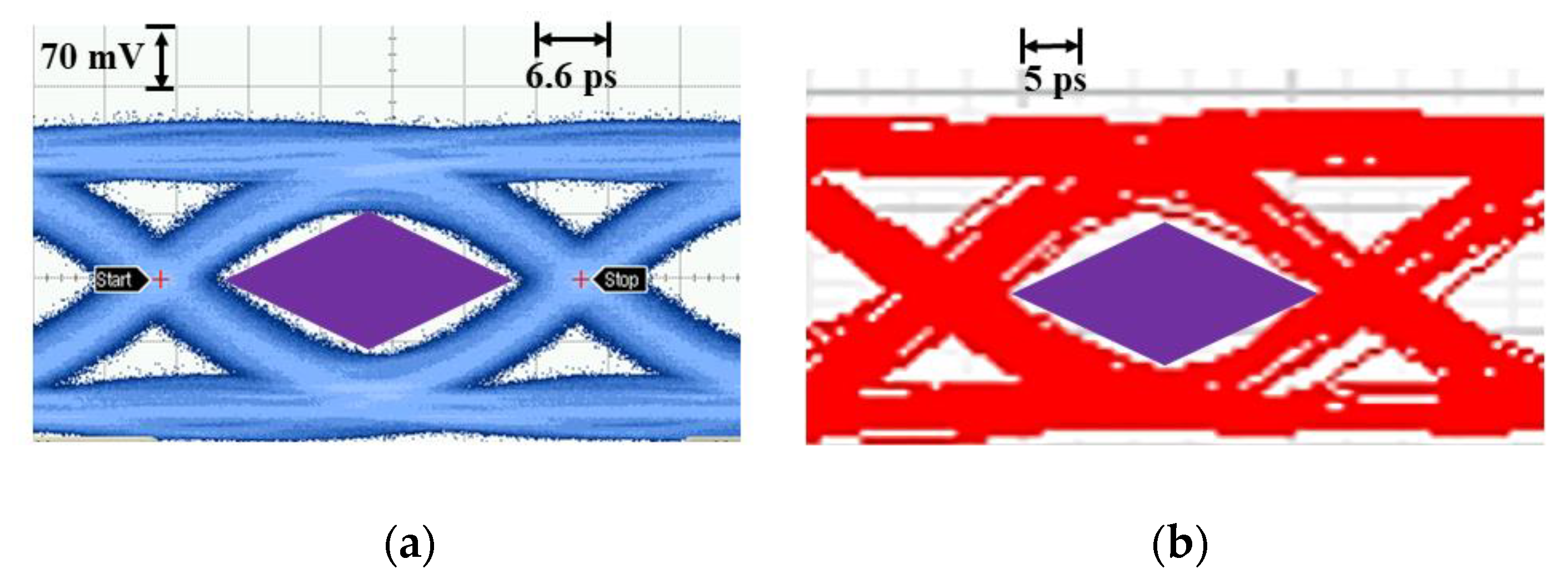
Table 3, the equivalent circuit model is realized in Cadence Tool Suits (Virtuoso Environment 5.10.41). The 25 Gbps PRBS-7 transient responses under 6 mA bias current for both simulation and measurement are shown in
Figure 7. The peak-to-peak jitter in the experiment is 11.3 ps, while the simulation result is 11.4 ps. The measured vertical and horizontal eye-opening ratios are 0.55 and 0.71, while the simulated ratios are 0.58 and 0.70, respectively. The measurement and simulation show satisfactory match, proving that the proposed model have strong ability to simulate the VCSEL performance.


