1. Introduction: Recombination Processes in Perovskites
The impressive photovoltaic performance of perovskites has made them one of the most promising high-efficiency photovoltaic materials. Perovskite-based solar cells have achieved power conversion efficiencies of 25.2% [
1]. The high performance of these materials can be attributed to the remarkable optoelectronic properties of perovskites: high absorption coefficient, long carrier diffusion lengths and low Urbach energy [
2]. Moreover, perovskites offer simple band gap tunability by changing composition and low-cost production. Despite the rapid progress of perovskite solar cells, they are still far from their full potential [
2]. The high absorption coefficient combined with device optimizations (at the electron and hole conducting layers) has led to increased light management and carrier collection and, therefore, minimized current loss. The voltage loss is also relatively small, but still below the theoretical limit. Similar to other thin-film semiconductors (GaAs, CIGS, CdTe), perovskite materials contain intrinsic defects, including point defects within the perovskite crystals and impurities at grain boundaries and surfaces [
3,
4]. As result of these defects, trap states for both electrons and holes can induce non-radiative recombination. This pathway of recombination for the photogenerated carriers is undesirable and lowers the voltage and, consequently, decreases the power conversion. To progress further toward the theoretical limit of power conversion efficiency, a better understanding of the defect states and knowledge of how to manipulate them is essential. Here, we consider the role of defects in perovskites, their chemical nature, and the defect chemistry. Next, compositional engineering as passivation method for defects within perovskite crystals is described, and reports on different mechanisms that are proposed to reduce the defect density and boost the voltage and PCE (power conversion efficiency) are analyzed. This review covers work published up to September 2019.
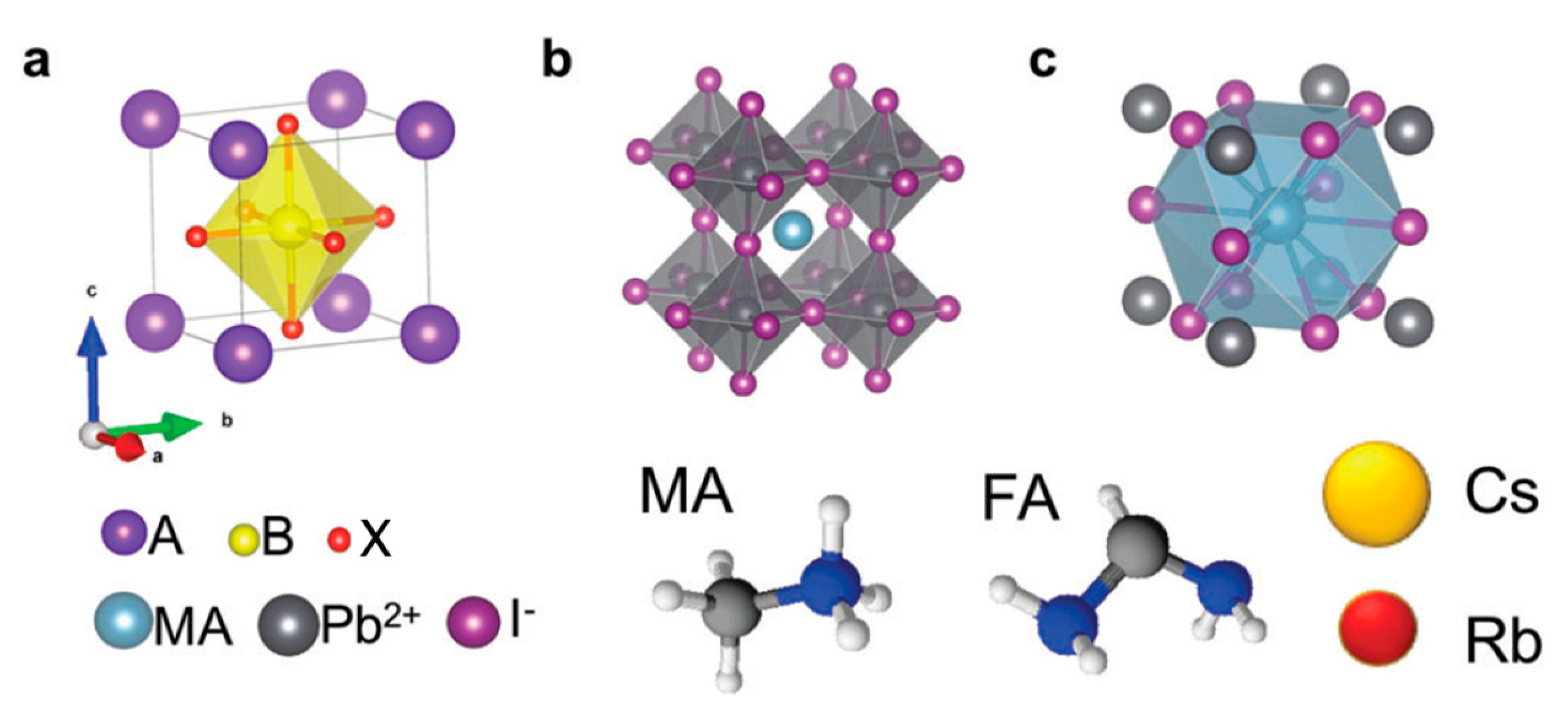
A perovskite solar cell is a type of solar cell that includes a perovskite material as light-absorbing layer. Perovskites possess the crystal structure ABX
3, where A and B are cations jointly bound to X, an anion (
Figure 1). One of the most investigated perovskites for solar applications is the methylammonium (MA) lead halide perovskite with the chemical structure CH3NH2PbXnY3−n (where X and Y are usually I, Br or Cl anions) [
5]. Perovskite materials are considered to be direct band gap semiconductors, and their band gap is primarily determined by the chemical composition and structure.
In a solar cell, the photovoltaic properties (open-circuit voltage (
VOC), short-circuit current (
JSC),
FF is fill factor) depend on the band gap and the charge transport. The carriers that contribute to charge transport are electrons in the conduction band (CB) and holes in the valence band (VB). The valence band is separated from the conduction band by forbidden energy levels [
6]. The difference between the conduction band minimum (CBM) and valence band maximum (VBM) is the band gap energy. The Fermi energy (Fermi level) is the electrochemical potential of the electrons, representing the average energy of electrons in the material. When incident light excites electrons from the VB into the CB this causes the splitting of the so-called quasi-Fermi levels of electrons and holes in a working solar cell. These levels describe the population of the electrons (in the CB) and holes (in the VB) separately, when their populations are displaced from equilibrium. The output voltage of the cell is determined by the difference of the quasi hole and electron Fermi levels [
6]. The open-circuit voltage (
VOC) is the maximum voltage generated by a solar cell, which occurs when no current flows through the external circuit (the forward bias voltage). Non-radiative recombination will create drainage for the recombination of excess free charge carriers and reduces the steady-state charge density, which reduces the splitting of quasi-Fermi levels and thus decreases
VOC. The relationship between the V
OC and recombination can be described by the external photoluminescence quantum efficiency (
PLQE), a measure for the fraction of radiative versus non-radiative decay (value between 0 and 1):
where
VOCrad is the radiative limit of the open circuit voltage when non-radiative (
non-rad) recombination is fully suppressed,
KB is the Boltzmann constant,
T is the temperature, and
q is the elementary charge. ∆
VOCnon-rad is the non-radiative open circuit voltage loss, the loss of voltage due to non-radiative processes.
VOCmax is the maximum attainable voltage. Moreover, recombination at surface and at grain boundaries also influences the charge extraction efficiency and could have an effect on the current collection, which reduces the short-circuit current (
JSC).
The voltage depends on the splitting of the electron and hole quasi-Fermi levels and therefore on the excess electron and hole carrier densities ∆
n and ∆
p, respectively (
Figure 2). These densities depend on free charge-carrier lifetime (τ), the time that electrons (holes) in the CB (VB) remain free, which is reduced by recombination.
We now describe the three most important recombination mechanisms [
3]. In radiative recombination (or direct recombination), an electron from the conduction band combines with a hole from the valence band. This mechanism has a higher probability for indirect band gap materials where there is no change in momentum required upon recombination or excitation from valence to conduction band. For direct recombination, we can assume that the rate (
Rrad) depends on the concentration of electrons (
n) in the conduction band and holes (
p) in the valence band:
Rrad = kr ×
n ×
p. Recombination can also be facilitated by impurities or lattice defects in Shockley–Read–Hall (SRH) recombination. These defects in the semiconductor structure introduce so-called trap states that can have energies that lie within the band gap. An electron (or hole) can be trapped at the recombination center and thereupon recombine with a hole (or electron) that is attracted. This is a non-radiative process and heat created during the recombination is dissipated into the lattice in the form of vibrations. The rate of SRH recombination is monomolecular:
RSRH =
kS ×
n. When there are three particles involved in the recombination process, this is called Auger recombination [
3]. Here, the recombining electron and hole transfer the energy and momentum to another electron or hole. If the energy is transferred to an electron, it is excited into higher energy levels in the conduction band. When it relaxes, the energy of the electron is transferred to vibrational energy of the lattice (phonon modes). A hole will be excited deeper into the valence band before it relaxes back. The rate equation can be expressed as follows:
Rauger = kA ×
n2 ×
p.
Figure 3 shows that the effective bulk lifetime in MAPbI
3 is dominated by SRH recombination at low carrier injection levels (up to ∆
n ∼ 10
15 cm
−3). At high injection levels (up to ∆
n ∼ 10
17 cm
−3), the bulk lifetime is mainly determined by radiative recombination [
3]. For perovskite solar cells under the condition of 1-sun illumination ∆
n corresponds to ∼10
16 cm
−3, resulting in relatively small Auger recombination rate constants (∼10
−28 cm
6/s) [
7]. Clearly, perovskite materials are usually more limited by SRH recombination. Auger recombination is in general not so important. Furthermore, Auger recombination is more prominent in indirect semiconductors (such as
c-Si) since radiative recombination is retarded as it requires interaction with phonons, while in Auger (and SRH) recombination energy and momentum is transferred. Thus, as a result of the direct bandgap and average charge-carrier concentrations, SRH recombination is the most relevant loss channel in perovskite under non-concentrated sunlight (1-sun illumination = 1000 Wm
−2 at AM 1.5).
The observed inverse of the bulk lifetime (
τbulk) equals the sum of the reciprocal radiative lifetime (
τrad), the lifetime determined by Shockley Read Hall recombination (
τSRH) and the lifetime determined by Auger recombination (
τAuger); the inverse of the effective lifetime is also determined by the lifetime related to surface recombination (
τsurface):
The carrier trapping into defect states leading to SRH recombination severely limits the quasi-Fermi level splitting and hence the photovoltage of solar cells [
8]. To understand the origin of SRH recombination, the density of defects but also their chemical nature, spatial and energetic distribution within the band gap is important.
Section 2 will go into detail about different defects that can create electron and hole traps. Before that, we will consider the Shockley–Queisser limit to see why it is important to decrease the SRH recombination pathway.
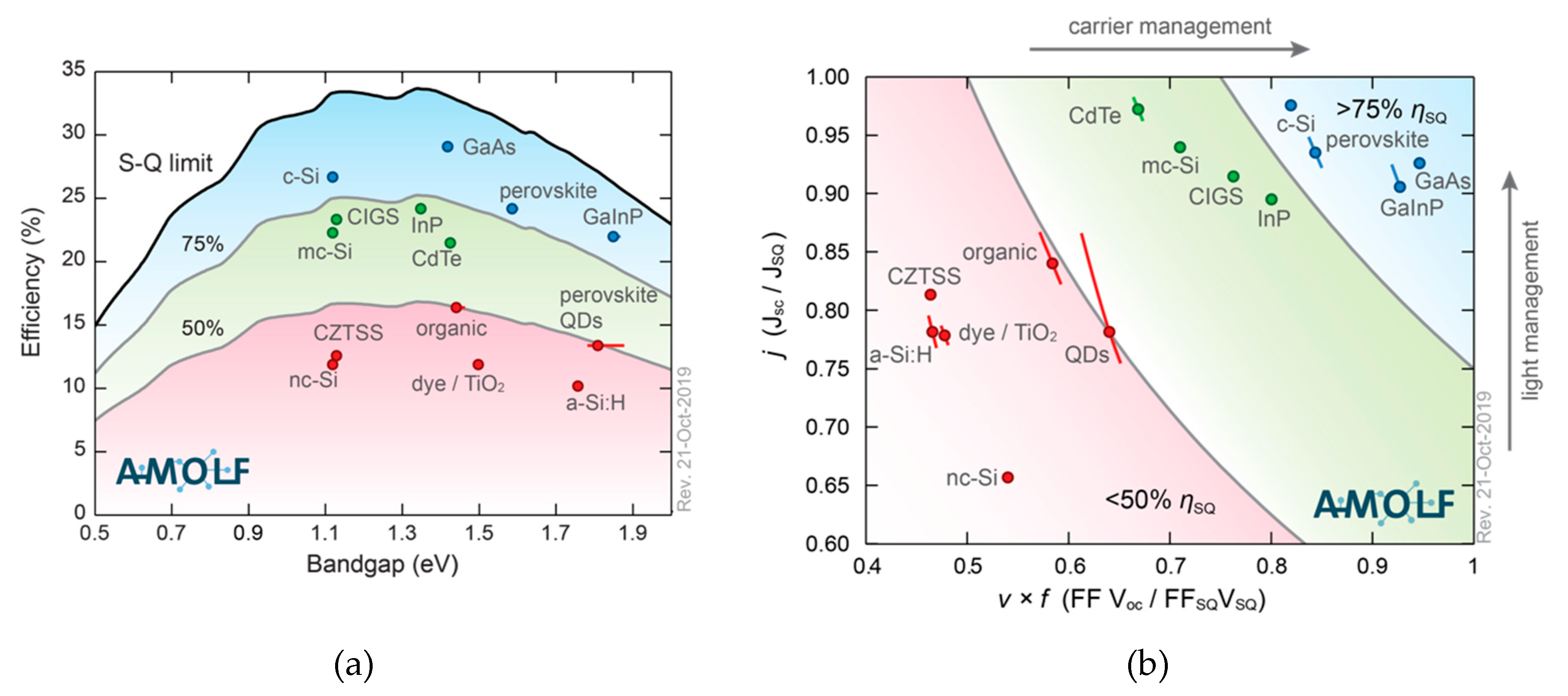
The Shockley–Queisser limit is widely used to define the theoretical maximum efficiency for single-junction solar cells [
9]. The limit is defined by three important assumptions: first, it is assumed that for each incoming photon with energy greater than the band gap an electron-hole pair is produced. Secondly, electron-hole pairs with energy in excess of the band gap lose this energy via thermal relaxation. Furthermore, the Shockley–Queisser limit takes into account that a solar cell is in (thermal) equilibrium with its surroundings. Therefore, a cell under operational temperature will emit (black body) radiation. The first two assumptions relate to the spectral match and interaction of the absorber material and the incoming sunlight. The “equilibrium state” also leads to unavoidable radiative charge recombination of electron-hole pairs causing the recombination current density to be non-zero. Since the absorptive transition is allowed, also the reverse radiative transition is allowed. In fact, for the ideal solar cell material, only the unavoidable radiative charge recombination should occur, and no non-radiative charge recombination whatsoever: it should be eliminated and is avoidable.
The Shockley–Queisser limit is useful to compare existing and novel photovoltaic technologies and their performances.
Figure 4a shows the record-efficiency cells for various materials plotted against their band gap, together with their regions, expresses as a percentage of the S-Q limit (in red [below 50%], in green [between 50% and 75%] and in blue [>75%]). Most photovoltaic materials are currently below 75% of their theoretical maximum efficiency while perovskite technology, with a record efficiency of 25.2%, is starting to compete with commercialized technologies like
c-Si (26.7%) [
1,
10,
11]. GaAs clearly still is highest in the graph.
Figure 4b shows that light management (which influences
JSC /JSQ) is relatively good in perovskite, meaning that current losses are low (93% of the maximum current for that band gap). The carrier management, the ratio of the FF ×
VOC to their theoretical maximum (FF
SQ ×
VSQ), is lower (0.80) for perovskites. Thus, in order to engineer perovskite towards the ultimate power conversion efficiency, optimization of the voltage (which is influenced by charge carrier management) is of great importance.
2. Defect States in Perovskite Materials
Several studies show that imperfections or defects in perovskites induce (high densities of) deep-level traps [
8,
12,
13,
14,
15,
16,
17,
18,
19,
20,
21,
22,
23,
24,
25,
26,
27]. These deep-level traps will trap either electrons or holes, that do not escape by thermal activation but will recombine non-radiative as described by Shockley–Read–Hall theory (see
Section 1). Shallow traps are defined as traps that lie closer to the CBM or VBM than the thermal activation (
KBT = 23.5 meV at 0 °C,
KBT = 29.6 meV at 70 °C) and are thus less detrimental to device performance. In this section, the different types of defects are discussed in depth. We will first highlight some experimental approaches to gain insight into the chemical nature of defects in perovskites. Next, several computational studies that describe defects and their photophysical properties on a more atomistic level will be discussed.
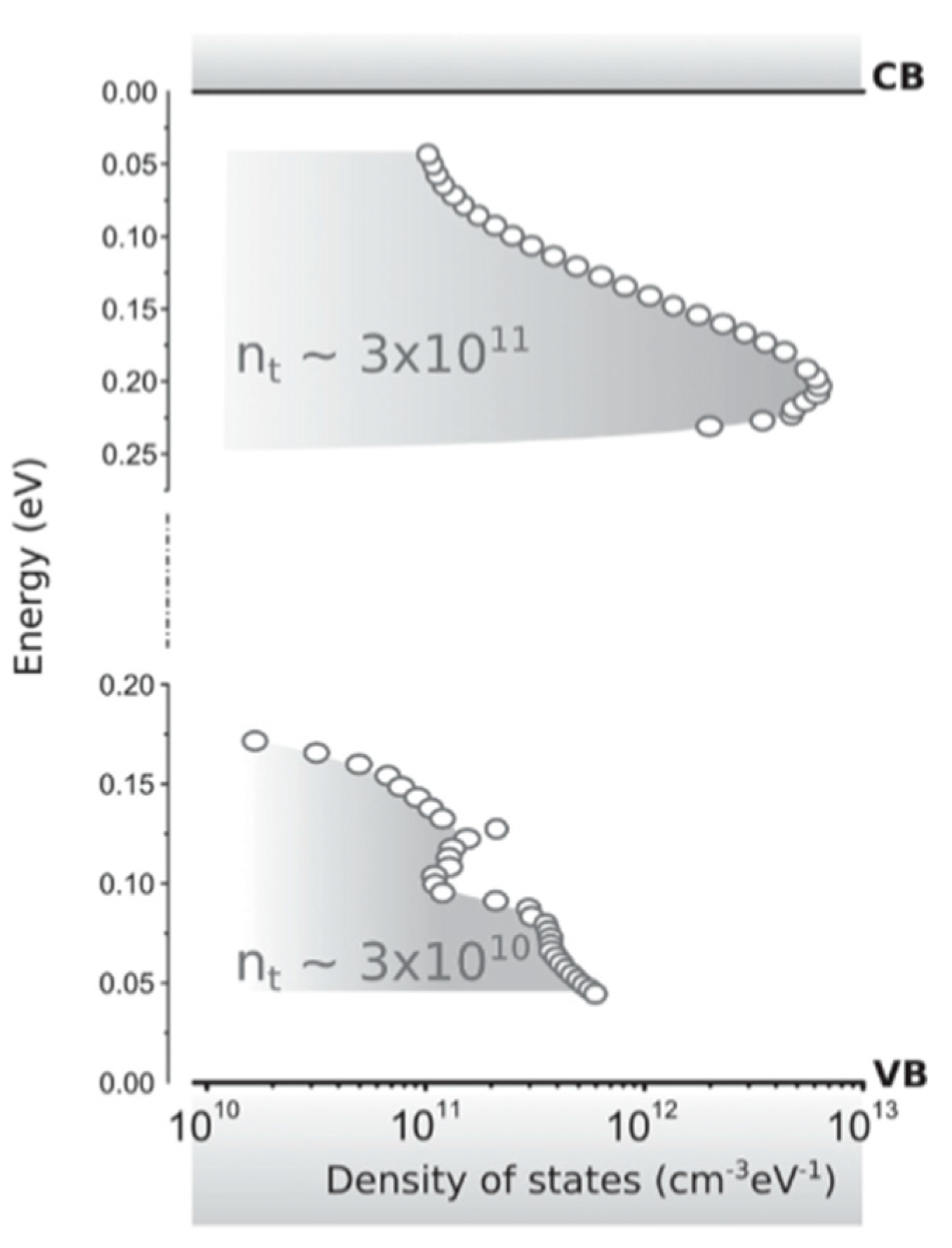
Adinofli et al. used temperature-dependent space charge-limited current (SCLC) techniques [
12]. With this technique, the density of trap states (
DOST) can be extracted from the current-voltage characteristics.
Figure 5 shows that for single-crystal MAPbI
3 the
DOST appears to be localized only ∼0.2 eV from the conduction band and ∼0.1 eV form the valence band. From this, it can be concluded that MAPbI
3 contains both shallow hole traps and shallow electron traps.
However, with a combination of transient and steady-state photoluminescence spectroscopy, Leijtens et al. analyzed carrier dynamics and showed that deep traps for electrons are the predominant decay pathway [
8]. Furthermore, using deep level transient spectroscopy the presence of charge traps placed in the middle of the band gap was observed [
13]. The chemical nature of charge traps has also been studied with several spectroscopic techniques. X-ray techniques usually focus on the perovskite structural parameters; common structural phase transitions can be observed as a function of temperature, including orthorhombic–tetragonal–cubic transformations. Combining x-ray and neutron diffraction experiments to analyze changes in bond distances, Minns et al. showed that for the tetragonal perovskite structural disorder can be associated with the formation of I
2 [
14].
Figure 6 shows a proposed mechanism: through the migration of iodine to a vacancy (MA vacancy at the lattice A-site) the I
2 molecule is formed.
Using X-ray photoemission spectroscopy (XPS), the formation of vacancies from the methylammonium site (V
MA) and iodine site (V
I) were shown. The loss of MA and I species did not lead to significant changes in photoluminescence properties of the material. This apparent defect tolerance was explained by the fact that the V
MA and V
I defect lie close to or within the conduction and valence band, respectively [
15]. In contrast, an early study that also used XPS showed that metallic Pb
(0) is present in the perovskite layer with high concentration in the bulk [
16]. This defect, resulting from V
Pb, was correlated to the density of states above the valence band. They also observed reduced PLQE when the Pb content was increased.
The experimental work discussed above demonstrates that (polycrystalline) perovskite can accommodate several different defects. However, to understand defects and their chemical nature on an atomistic level, computational modeling has become an essential tool. Density-functional theory (DFT) is a high-end computational method, a quantum mechanical modelling method that derives properties of molecules and materials based on a determination of the electron density of the molecule, based on functionals of the spatially dependent electron density. Several computational studies on perovskite crystals employing DFT have been carried out in the past few years, which successfully characterized various defects, called point defects [
4,
14,
17,
18,
19,
20,
21,
22,
23]. A crystal structure can accommodate several of these point defects which are defects at a single lattice point, not extended in space in any dimension. Here, we distinguish between the following type of point defects that are frequently reported in perovskite material: Vacancies—when one atom leaves its lattice site; Schottky defects—when two oppositely charged ions leave their lattice sites; interstitial defects—when an atom occupies a site in the crystal structure at which there is usually not an atom; substitutional defects—when an impurity atom is incorporated at a regular atomic site in the crystal structure; anti-site defects—when atoms of different type exchange positions.
Using DFT, the stability of the defect can be evaluated by calculating the defect formation energy (DFE). The stable charged states of a defect can be obtained by analyzing the DFE as function of the Fermi level. From this the thermodynamic ionization levels between different charged states of a defect (q/q’) can be calculated, which is defined as the Fermi level where DFEs of two charge states are equal (DFE(Dq) = DFE(Dq’)). Negative defects can capture holes (acceptors, q0/q−) and positive defects can capture electrons (donors, q0/q+). Neutral defects can be ionized by the capture of electrons or holes. The thermodynamic ionization level corresponds to the oxidation and reduction potential of the defect and its position with respect to the VBM and CBM determines whether the defect will act as a (shallow or deep) trap for photogenerated carriers.
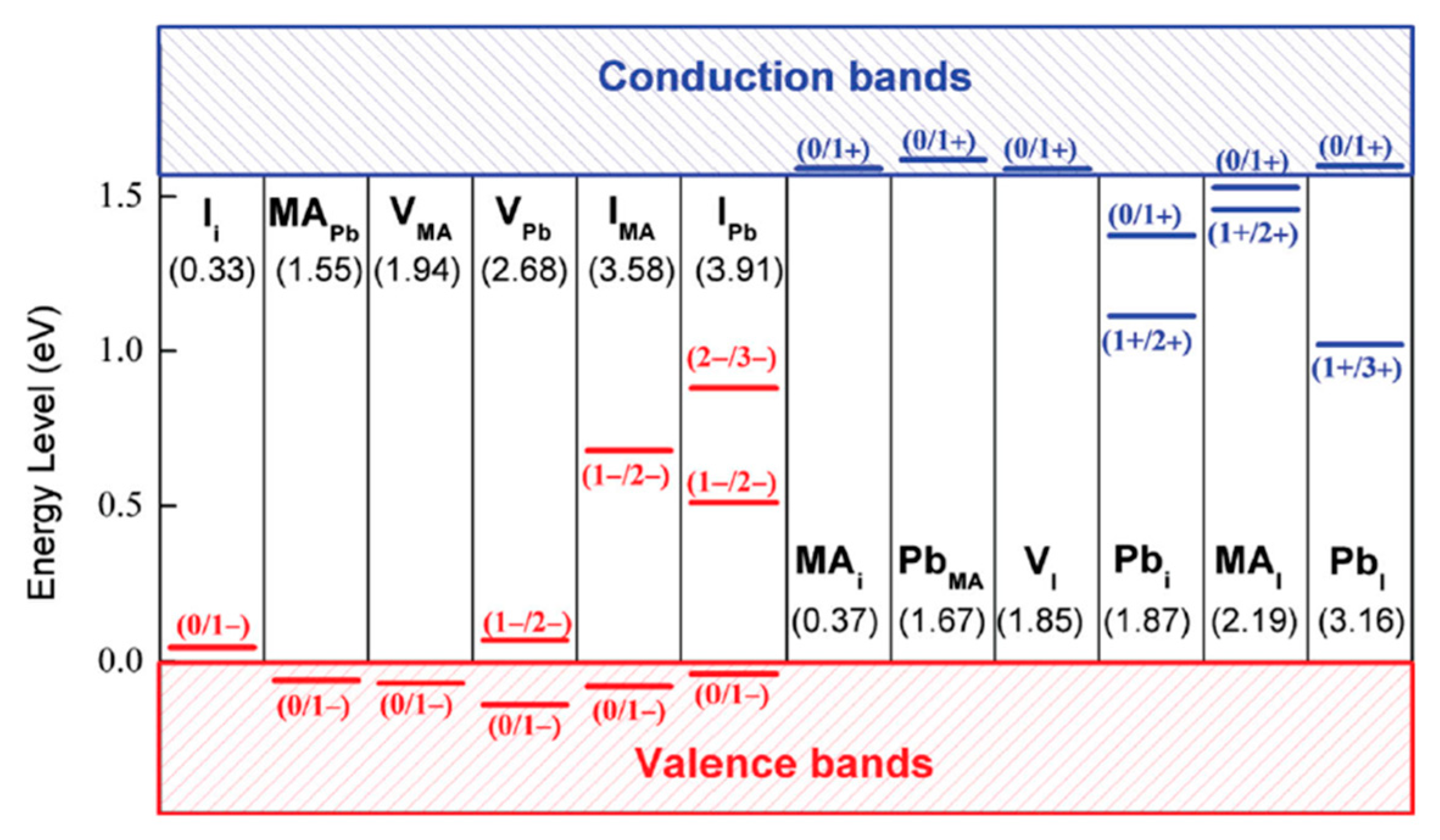
Figure 7 depicts transition energy levels and the DFEs for point defects in MAPbI
3 calculated by Yin et al. using first-principle calculations [
17]. They identified the following defects with low formation energies that can be found near the valence band (acceptors): Iodine interstitials (I
i), MA substitutional defects (MA
Pb) and vacancies (V
MA and V
Pb). In the conduction band they found that MA
i, Pb
MA, and, V
I with low formation energies. These defects all have transition energy levels within or close above (under) the valence (conduction) band and are, therefore, considered to be shallow defects. Moreover, the defects with deep transition levels have relatively high formation energies. These results suggest that deep level traps are less predominant than defects that create shallow traps. Some defects have transitions where, for example, 2 electrons are involved (Pb
i, (1+/3+)). These defects have low capture cross sections which makes trapping more unlikely.
Similar to Yin et al. other theoretical work suggests that Pb
2+, I
− and MA
+ vacancies are predominant and only create shallow traps [
18]. On the other hand, it can be argued that simple trapping and un-trapping of photogenerated charge might not give a complete picture. The slow charge carrier dynamics and stability-threatening phenomena, such as current-voltage hysteresis, are not readily explained by the presence of shallow traps and only the limited amount of deep level traps. Ion defect transport has been widely observed in perovskite material and is another possible origin that potentially lowers power conversion or even device stability. DFT simulations have shown that ionic disorder in perovskite leads to low formation energies for Schottky-type defects associated with anion and cation vacancies [
19].
Eames et al. carried out calculations in order to examine the pathways and relative activation energy for the vacancy-mediated migration of the cations and anions [
4]. They proposed a hopping mechanism, as shown in
Figure 8.
Using transition-state calculations between adjacent sites, they mapped out energy profiles for these mechanisms. The lowest activation energy was found for iodide ions, which was 0.58 eV compared to 0.84 eV and 2.31 eV for MA
+ and Pb
2+, respectively. The authors suggested that iodine vacancy-assisted diffusion is favorable since this migration pathway is more ideal as it does not involve motion through the unit cell and they argued that the high activation energy for Pb
2+ rises from the immobile Pb sub-lattice. Other theoretical work supports the proposed general mechanism; the ion mobility is directly related by the transport activation energy and the hopping distance [
20]. In these studies the iodine ion is also confirmed as the most mobile ion [
20,
21].
Recently, iodine interstitial defects were identified as the main source for trapping electrons and holes in MAPbI
3 [
22,
23]. These results showed significant differences with previous studies (
Figure 7) [
17,
24]. Where early studies proposed that defects with low formation energies that form shallow traps are predominant, more high-level calculations based on hybrid DFT showed that iodine interstitials, in fact, induce deep levels in the MAPbI
3 band gap [
23]. Meggiolare and co-workers performed DFT calculations that included both dispersion correlation corrections and spin-orbit coupling. They calculated that interstitial iodine can lead to a deep trap for both electron and holes at the +/0 and 0/− ionization levels placed at 0.57 and 0.29 eV below and above the CB and VB edges, respectively [
22].
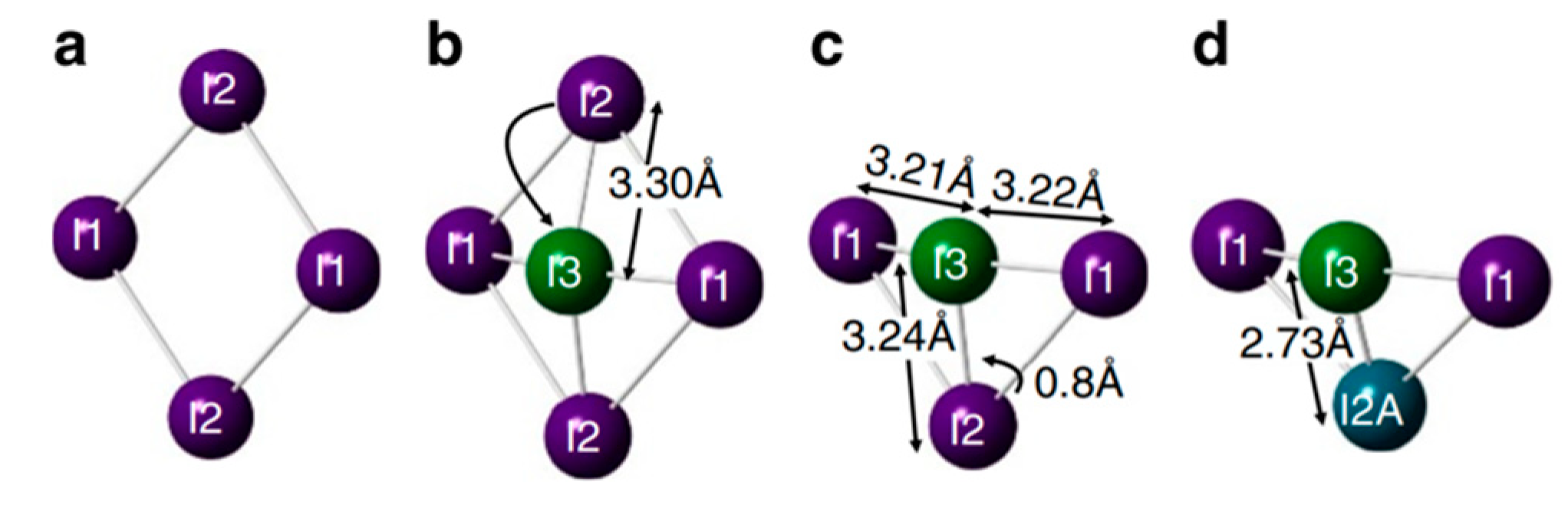
In addition, Meggiolare et al. studied the photochemistry of the defect states. The various charge states of interstitial iodine (I
i) result in different local geometrical structures:
Figure 9a shows the positive I
i+ state, resulting in a trimer structure of a coordinated I
3—molecule, this is an electron trap (+/0); the neutral I
i0 state (
Figure 9b), here iodine formed a bridged dimer; and a negatively charged I
i−, which is a hole trap (0/−) with a similar structure to that of I
i0 (
Figure 9c).
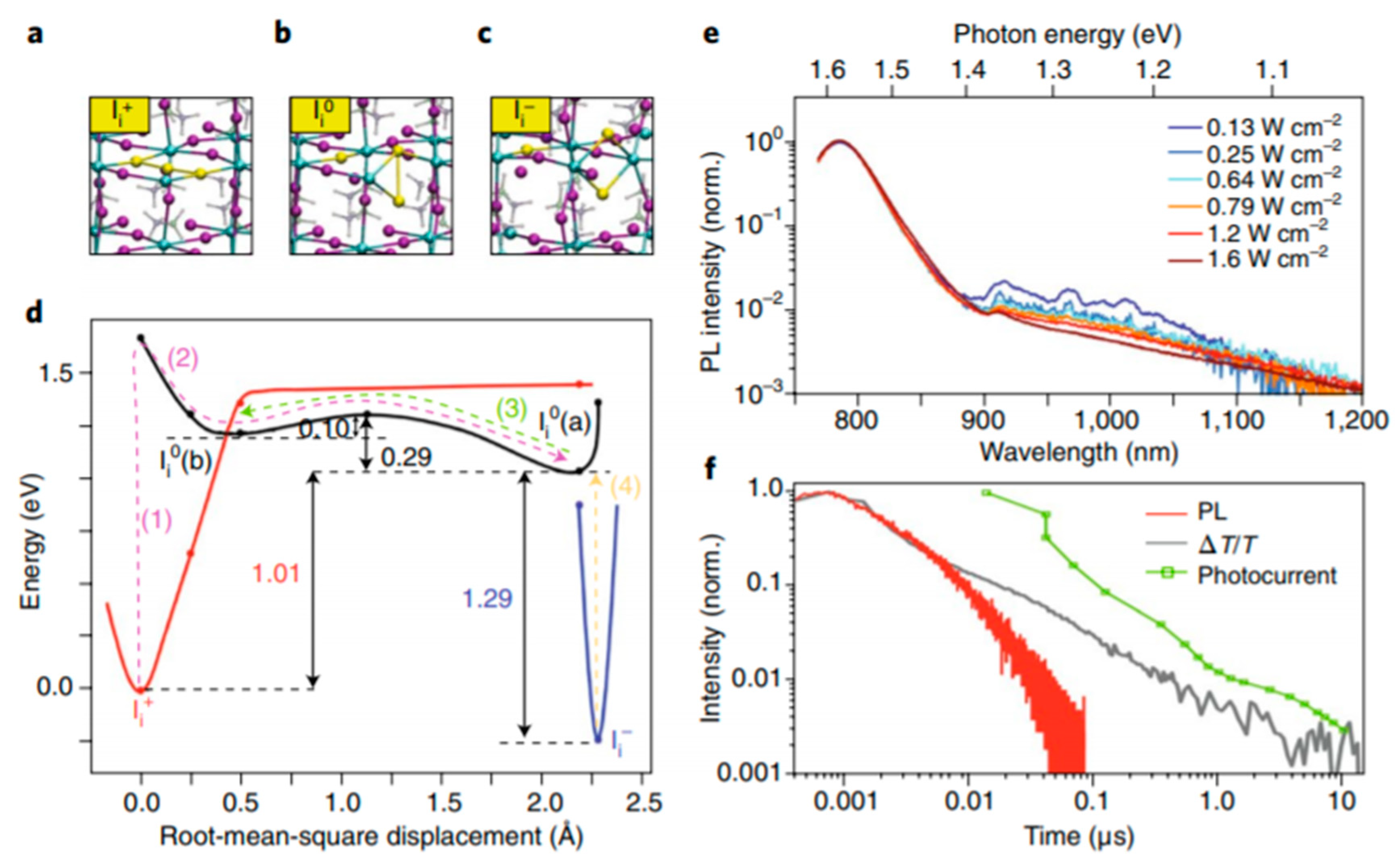
Using the description of the minimum energy structures corresponding to each charged state of interstitial iodine, the reaction pathways (trapping pathway) can be visualized according to a global configuration diagram.
Figure 9d shows that the energy minima of the three states have significantly different structures. This means that when the defect traps (or un-traps) charge, this is accompanied by large structural changes (as expressed by the root mean square displacement). In
Figure 9d we can see that the trapping of an electron in I
i+ (this process is marked with (1) in red) results in a structural relaxation to the I
i0 (a) global minimum, depicted in black, formed by process (2). The thermodynamic barrier is only 0.10 eV above the I
i0(b) local minimum. Process (3) depicted in green marks the pathway to un-trap the electron to go back the I
i+ state. If a hole is trapped, depicted in yellow by the process (4) to form the I
i0 (a) state, there is no barrier and structural rearrangement is limited. From this, it can be concluded that hole trapping and un-trapping is a fast process. It is expected that the large lattice reorganization for electron trapping at positive interstitials, results in long timescales for trapping and recombination.
To support the computational findings, steady-state photoluminescence on MAPbI
3 poly-crystalline thin film was used. Since interstitial iodine traps are sub-band gap states, this means that radiative recombination (emission from trapped holes) should be observed at energies below the band gap.
Figure 9e, in fact, reveals weak emission in the 1.35–1.15 eV range, below the radiative recombination from the band gap (1.58 eV). Also, at increased excitation energies, quenching of emission is observed. This is expected from radiative trap-assisted recombination since increasing excitation will saturate the traps, which have no time to recombine radiatively.
Figure 9f shows the photoluminescence, which corresponds to the fast band-to-band radiative recombination. There is also a slow component which does not match any radiative feature, but follows the photo-current, and therefore is suggested to rise from non-radiative recombination of free holes with electrons trapped by I
i+ (arrow (3) in
Figure 9d).
If electrons are trapped, it takes a long time before they recombine and therefore they will remain inactive for a long time. Trap filling for a long time reduces the effective trap density, which has direct implications on the V
OC. Leijtens et al. determined the quasi-Fermi level splitting by estimating the steady-state carrier dynamics and with this calculated the V
OC for different trap situations (
Table 1) [
8]. In the ideal case of defect-free perovskite, when only bimolecular recombination occurs, the V
OC is 1.30 V. Short-lived carriers reduce the V
OC to 1.14 V; whereas increasing the lifetimes of the holes increases this value by 0.12 V, creating a V
OC close to the Shockley-Queisser limit.
The presence of trap states in the form of lattice defects has been widely observed. However, it is still not completely understood what defect states are the most predominant and play the most crucial role in non-radiative recombination. Based on current literature we can conclude that iodine vacancies are a predominant defect and could lead to iodine transport, but that trapping of holes and electrons is maybe more likely to occur at iodine interstitials. However, electron trapping with long lifetimes can also have positive influences on the V
OC. Furthermore, the role of environmental factors, such as atmosphere and light, are beyond the scope here but are an important topic for further understanding of defect behavior. For example, light soaking has been reported to decrease trap densities, but is also recently reported to increase hole trap states, which can be deactivated using oxygen [
26,
27]. Defect chemistry, its nature, and its dynamics will continue to be important ongoing topic. There is a growing body of literature in which non-radiative recombination is reduced, entailing distinct routes toward defect-free perovskite materials. These include the following: chemical surface treatments, light soaking, low temperature, and compositional engineering [
27]. Recently, the latter has gained more attention because of the following two reasons: (1) compositional engineering can aid high-quality film formation; (2) using compositional engineering not only the crystal quality can be enhanced but also optoelectronic properties can be tailored.
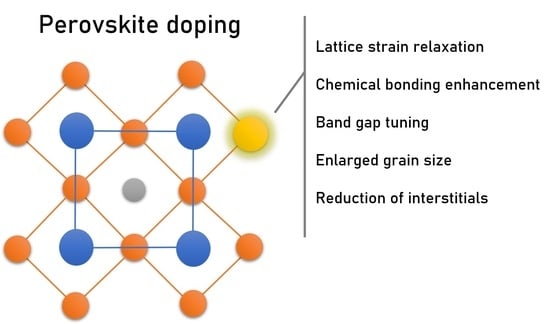
3. Defect Passivation through Compositional Engineering of Perovskites
Compositional engineering [
27,
28,
29,
30,
31,
32,
33] has become an attractive approach to optimize perovskite structure because of the advantage of directly tailoring other intrinsic material properties, which enables higher-quality perovskite with enhanced photovoltaic performances. Reference [
34] contains a condensed historic representation of compositional changes related to record perovskite devices (see Table 2 of reference [
34]). We can distinguish between two types of additives: Inorganic (metal cations and inorganic acids) and organic additives (small molecules, polymers, and fullerenes). Most additives can control the crystallization of perovskite in some way and, therefore, enhance stability [
28]. However, organic molecules generally only passivate defect states at the surface and not do not alter intrinsic material properties, while the bulk trap density might be reduced by the incorporation of inorganic molecules into the lattice. In literature a variety of dopant- effects that enhance perovskite performance are reported [
28,
29,
30,
31,
32,
33,
34,
35,
36,
37,
38,
39,
40,
41,
42], which can be divided into influences on the crystallization and influence on the intrinsic lattice properties. Most effects described in literature are still not well-explained making rational compositional tailoring challenging. Here, current literature on Zn(II) and several other inorganic dopants are reviewed with the aim to obtain a more mechanistic picture on how dopants affect different properties and control the defect density.
A considerable amount of literature has been published on the use of inorganic dopants that improve photovoltaic performance of perovskite materials and many attribute this to the improved crystallization of doped perovskite [
29,
33,
34,
35,
41]. While the enhanced crystallization mechanisms do not seem to be fully understood, we review here several studies on dopants that effectively improve crystallization, leading to larger crystal domains and reduced defect density, and identify mechanisms behind this dopant effect.
Wang et al. discovered that Al
3+, at low concentrations (<0.3%), facilitates crystallization of MAPbI3, and specifically enhanced the growth of the (
hh0) crystal plane [
29]. This was ascribed to reduced micro-strain in the lattice during the crystallization process, resulting in better oriented crystalline domains and consequently a reduced density of defects. Crystallography and mass spectrometry revealed that Al
3+ was not significantly incorporated in the lattice, which is expected from the ionic radius (53 pm and 199 pm for Al and Pb, respectively). Crystal defects that potentially occur in the form of terraces are reduced via a selective growth of these terraces induced by Al
3+.
Unlike Al
3+, Zn
2+-ions have been proven to be incorporated at the lattice B-site, replacing lead ions. Chen et al. argued that this incorporation leads to better crystallization of MAPbI
3 perovskite [
30]. Using X-ray diffraction (XRD) they showed successful doping of the perovskite and with attenuated total reflectance Fourier transform infrared spectroscopy (ATR-FTIR), they demonstrated that the interaction of the Zn
2+ and MA ions are stronger in comparison to the Pb-MA interaction. Upon 0.1% Zn
2+ doping of MAPbI
3, photovoltaic performances were increased the most. This was attributed to higher chemical interaction and coordination between Zn
2+ and anions, and the organic group, which makes the doped system tend to grow into larger grains. They also observed an
over-doping effect for high Zn
2+ concentration, which was believed to result in the accumulation of bigger grain seeds on the previous small grain seeds affecting the general coverage and therefore reducing the photovoltaic performances.
In contrast to these studies, other work shows that the relation between optoelectronic quality and the orientation and size of crystalline domains must be interpreted with caution. Muscarella et al. (2019) used electron back-scattered diffraction (EBSD), which has higher spatial resolution than the conventional XRD and scanning electron microscopy (SEM) methods, to obtain crystallographic parameters [
31]. They correlated the results with local photoluminescence properties. The PL and carrier lifetimes did not show any dependence on grain size or orientation. They argued that the contrasting findings with previous studies can be explained by the following: First, morphological clusters observed in SEM and real crystallographic grains are often misinterpreted, clusters seen in SEM can be wrongly assigned to grains. Secondly, the chemical additives that create enlarged grains and preferential orientation can also passivate defects or grains.
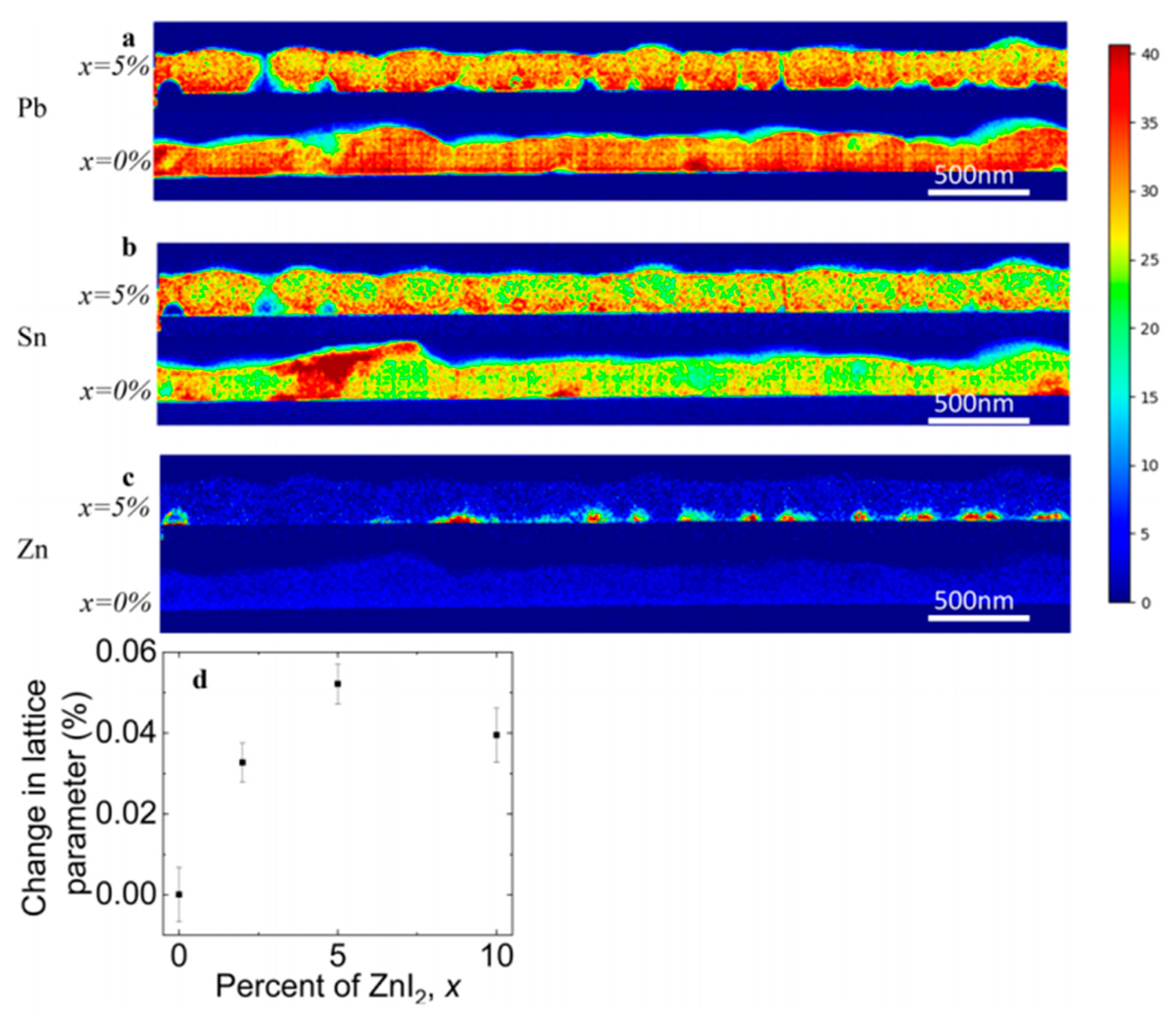
Also Bowman et al. (2019) showed that zinc does not necessarily influence the crystal grain size or orientation but can aid homogeneous incorporation of elements [
32]. Lead-tin based perovskite cells were fabricated employing different concentrations of ZnI
2 precursor and from the chemical spatial distribution mapping of the elements (by using STEM/EDX = Scanning transmission electron microscopy / Energy-dispersive X-ray spectroscopy), as shown in
Figure 10, it was observed that Zn doping leads to more homogeneously distributed Sn through the films (
Figure 10b). The majority of the Zn localizes along the bottom of the film (
Figure 10c) and, therefore, they proposed that high doping concentration can form an insulating layer. This also explained the current and voltage enhancement for the 1% and 2% ZnI
2 doping devices and the decreasing device performances at 10% doping. The XRD results revealed a small increase in the lattice parameter so that it is expected that Zn is incorporated in small amount but that the structure is not altered nor its grain sizes. They speculated on the role of Zn as an active dopant, as suggested by Saidaminov et al. [
33], and as additive assisting and seeding the growth of higher-quality grains that are chemically more homogeneous.
When perovskite material is tolerant to the inclusion of extrinsic dopant, additional passivating effects are observed. Here, we discuss several dopants that are able to incorporate on either the A, B, X-site or at interstitials and the subsequent influence on the lattice. The tolerance for the inclusion of foreign atoms by the perovskite lattice depends on the ionic radius. Small amounts of extrinsic doping at the A, B, X sites in the perovskite crystal can lead to increased disorder if the radius is either too large or too small. These lattice distortions affect the phase stability of the perovskite as empirically described by the Goldschmidt tolerance factor:
where
r are the ionic radii and 0.8
< t < 1 to maintain the 3D perovskite lattice, with a perfect cubic base at ideal 1. For MAPbI3 the reported factor ranges between 0.92–0.95. The incorporation of Zn at the B-site has been frequently reported and can also be expected from the calculated tolerance factor of 1.05 for MAZnI
3 [
34]. Shai et al. argued that the incorporation of Zn(II) in MAPbI
3-xCl
x crystals caused the lattice to shrink, they observed contraction of
BX6 octahedron, which is beneficial to fix the A-site cation and relax the lattice strain [
35]. This also promoted the formation of ordered and uniform perovskite crystal with tetragonal structure. They ascribed the formation of more stable perovskite to the increased electron-donating ability at the B site, creating stronger B-site–X-site interactions.
Chemical bond enhancement can also be achieved through doping with more electronegative halides. Li et al. fabricated a triple-cation perovskite (Cs0.05FA0.54MA0.41)Pb(I0.98Br0.02)3 and used several halides for doping, NaX (X = I, Br, Cl or F), in a two-step solution process [
36]. All alkali halides improved the quality of the perovskite, with the fluoride-containing material (0.1%) giving the best performance. Time-resolved PL showed increased carrier lifetimes implying that non-radiative recombination is suppressed. The increased electronegativity of the fluoride anion was argued to result in a stronger ionic bond with Pb and in formation of a hydrogen bond with FA ions, leading to stabilizing of local structure and inhibiting mobilization of ions (I and MA/FA). Hydrogen bonding between the NH of the organic ion and the F ion was confirmed by
1H-nuclear magnetic resonance (NMR). The F ions did mainly occupy the surface and grain boundaries. In contrast to the other ions, devices with F
− ions exhibit negligible
J-V hysteresis, indicating that the chemical bond enhancement with F immobilizes the counter ions. The stabilization reported by Shai et al. resulting from lattice shrinking can be explained by the strain in the pristine perovskite lattice. Lattice strain in MAPbI3 was first observed by Huang et al. in high-temperature annealed thin films MAPbI
3 perovskite [
37]. Using XRD and temperature-dependent conductivity measurements, they correlated ion migration to increased lattice strain. Saidaminov et al. speculated that lattice strain is at the origin of vacancy formation [
33]. DFT calculations showed that the formation energy of lead iodine vacancies was increased upon replacing FA and I with the smaller Cs/MA and Br.
They argued that if the size of the A cation does not match the lead halide octahedral cage, strain will be present in the material. When local strain acts on the lattice, strain can be released through the formation of point defects or by incorporation of small ions. Especially in FAPbI
3, where size mismatch is largest, this strain is likely to be reduced by point defect formation since the calculated formation energies lie close to 0 eV. The strain relaxation through the formation of vacancies has also been observed in oxide perovskites [
38].
Saidaminov et al. successfully incorporated Cl
– into the lattice of triple-cation perovskite films (CsMAFAPbI
2.55Br
0.45) [
33]. They observed increased long term stability and reduced superoxide generation, which indicates that Cl reduces the density of defects. Using DFT calculations, they found ∼0.3 eV increase in formation energies for iodine vacancies. Computations also showed that the Pb-X bond length decreased, as did Pb-X-Pb distortion angles. Therefore, they proposed lattice strain relaxation as reason for reduced iodine vacancies. The downside of the substitution with small halogen anions is the widening of the band gap [
39]. Although incorporation might reduce non-radiative recombination, it will lower the device efficiency because of a sub-optimal band gap. Furthermore, the incorporation of Cl ions inside other perovskite lattices, such as the MAPbI
3, has been unsuccessful as the energetically more favorable location is outside the lattice [
40]. In order to relax strain further at the B-site, Saidaminov et al. incorporated Cd because it is isovalent to Pb but has a smaller ionic radius. DFT calculation showed that Cd incorporation relaxes lattice strain and suppresses the formation of I vacancies by ≥0.5 eV. The Cd incorporation also increased the PL intensity of films tenfold.
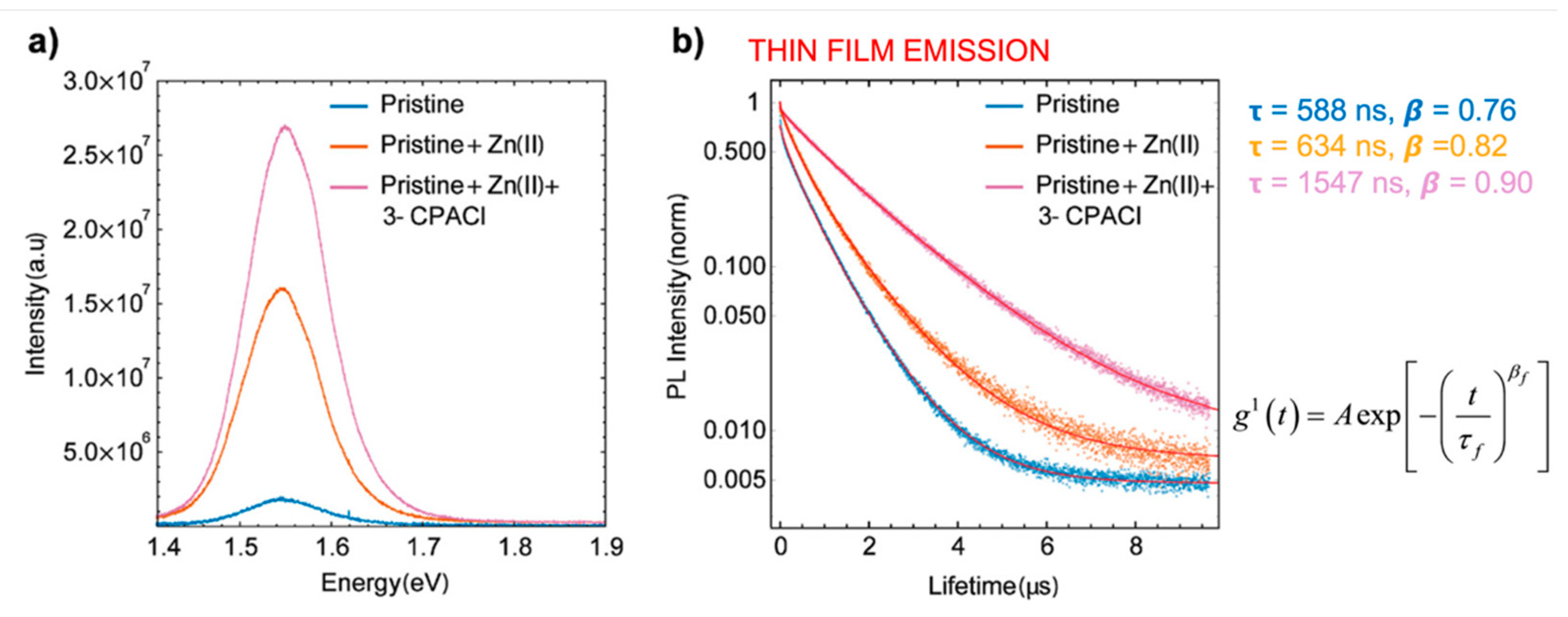
Similar effects have been observed [
41] upon doping with Zn(II) in combination with Cl
−, the latter originating from the alkyl-ammonium additive (see
Figure 11).
Lattice distortions can also implicate the perovskite band gap (
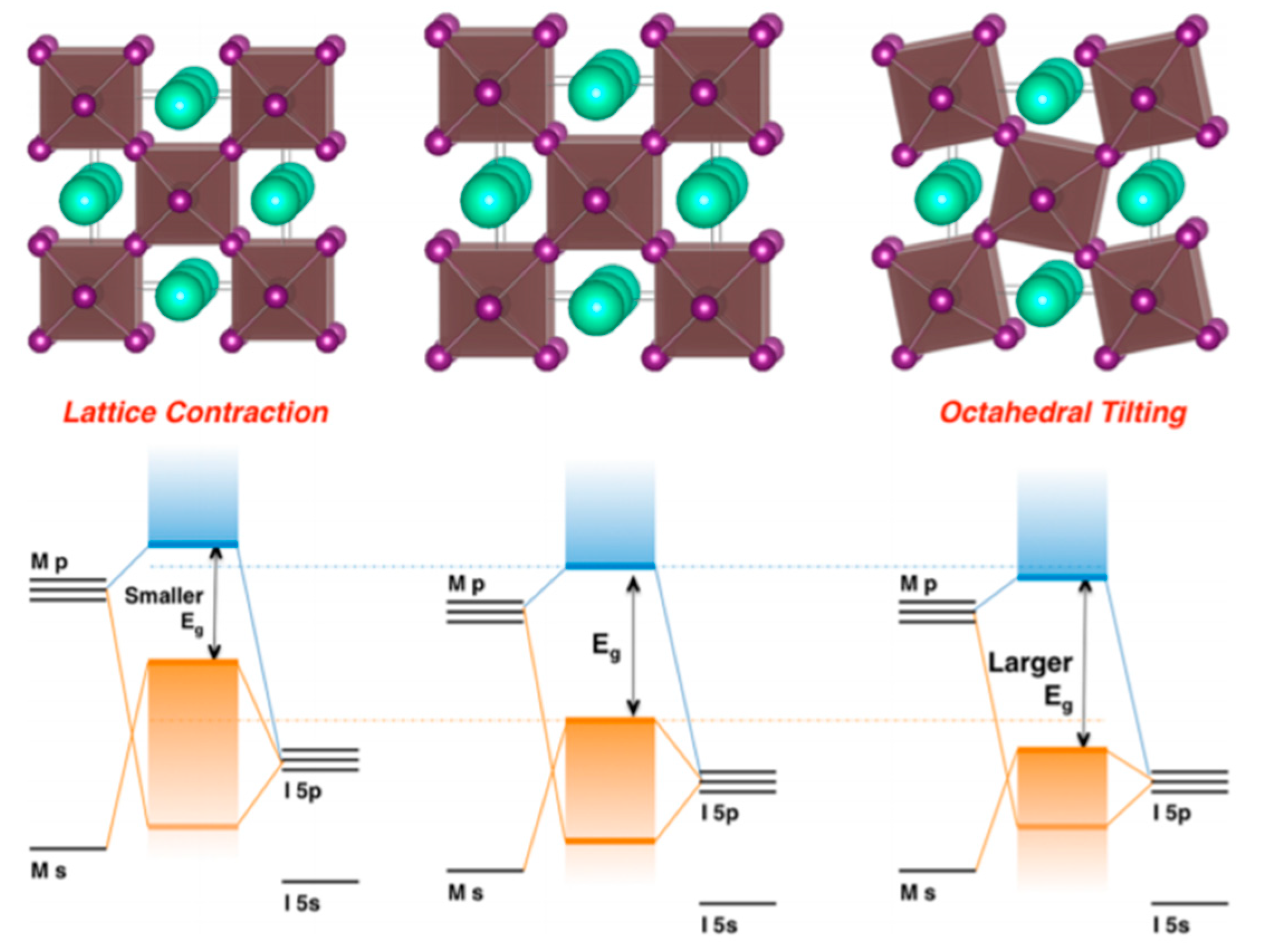
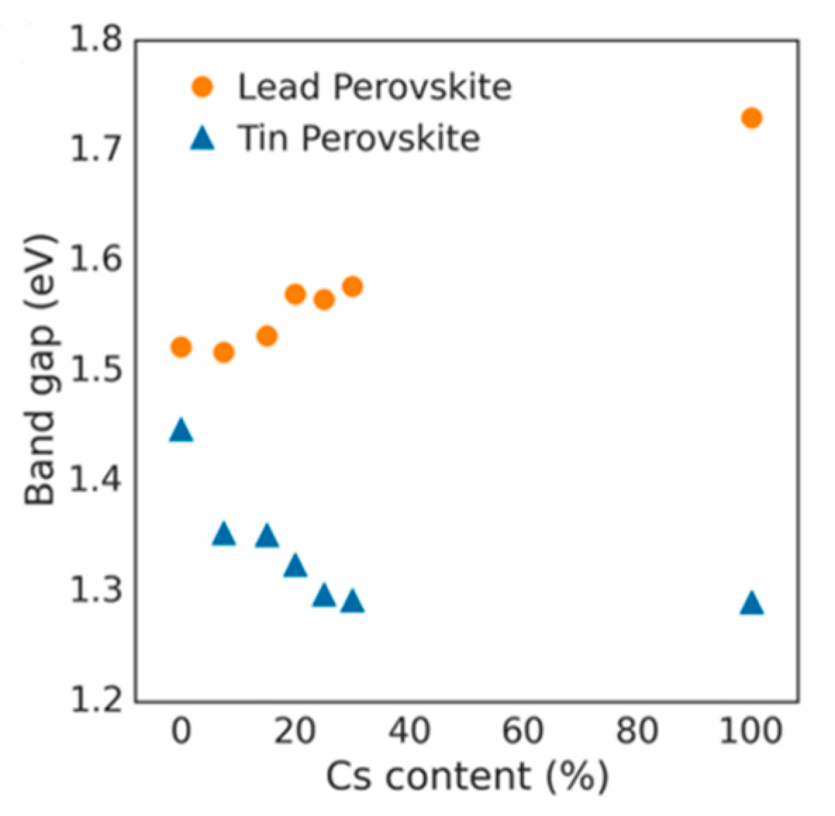
Figure 12). Prasanna et al. successfully incorporated Cs in Pb and Sn-based (FAPb/SnI
3) perovskite and observed that the for tin-based films introduction of Cs at the A-site decreased the band gap; whereas in lead perovskite films, introduction of Cs was observed to increase the band gap [
42]. They used grazing incidence X-ray diffraction (GIXD) measurements and revealed the incorporation of Cs has different effects in these two materials (
Figure 13). The tin iodide perovskite maintains its cubic crystal structure if FA is partly substituted by Cs and the only observed change is the isotropic contraction of the lattice. However, “in the lead iodide perovskite, additional X-ray diffraction peaks are observed, indicating that the structure experiences tilting of the BX
6 octahedra in addition to lattice contraction. Electronic structure calculations have shown that the VBM of perovskite material is an antibonding hybrid state of the metal s and halide p orbitals, and thus is sensitive to B-X orbital overlap (more than the CBM)” [
42]. This explains the different band gap response observed in the tin iodide vs. lead iodide perovskites.
In the former, lattice contraction increases orbital overlap, raising the antibonding VBM and the optical band gap is decreased. “In the latter, octahedral tilting decreases orbital overlap, moving the VBM to deeper energies and causing the band gap to increase. Band gap energies were directly measured with ultraviolet and X-ray photoelectron spectroscopy (XPS) and the results support this model” [
43]. Thus, for Cs doping at the A-site competing effects of octahedral tilting and lattice contraction were observed. When the X and B sites are doped, the electronic contributions of the dopant give rise to more complicated band gap interference.
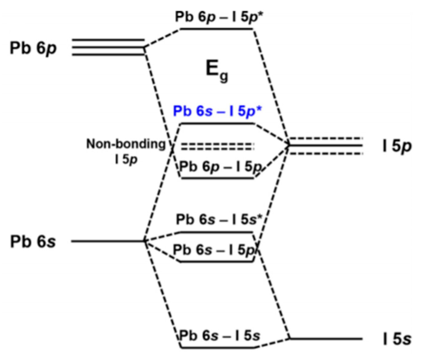
Figure 14 depicts the orbital contributions of the PbI framework to the band gap of MAPbI3. “The top of the valence band consists of an Pb 6 s—I 5p * anti-bonding hybrid state of the metal s and halide p orbitals. The conduction band minimum is a hybrid of metal 6p and halide 5p orbitals with less anti-bonding and more non-bonding character” [
44]. For dopants at the X-site in particular, the tuning of halogens has been frequently reported. Increasing the electron binding energies, for example from I to Br (from 5p to 4p, respectively), the band gap can be tuned from 1.5–2.3 eV by varying x in MAPb(Br
x I
(1−x))
3 [
45]. However, the band gap does not change linearly indicating increased defect densities upon Br introduction. B-site dopants are reported to infer with the conduction band. The replacement of lead with, for example, tin in MAPbI
3 widens the band gap [
46]. However, tin has also led to instability because of oxidation to the IV oxidation state. A recent literature review of Zn doped MAPbI
3 perovskite shows that generally the 3% doping leads to the most enhanced emission intensity and lifetimes, creating PCEs between 18%–20% [
34]. The band gap for low concentrations like this remains virtually unchanged [
47], with valence bands shifting from −5.45 to −5.50 eV upon going from 0 to 10% Zn(II) doping. Conduction bands shifting from −3.85 to −3.91 eV in the same doping range.
4. Discussion and Conclusions
With this work, the current understanding of intrinsic defects and their passivation in lead halide perovskites has been reviewed. Intrinsic defects in the perovskite bulk are at the origin of reduced V
OC by creating non-radiative recombination centers. Recent research has shown that the most important defects are iodine interstitials, which create effective hole and electron traps. The redox chemistry of the electron traps explains the apparent defect tolerance of lead halide semiconductors, deactivating the traps over longer times. However, other research highlights the formation of vacancies, which might create shallow traps but are reported to be mobile, affecting the stability and photovoltaic performances. We show that the addition of computational methods is essential to predict the stability and density of point defects. Combined computational and experimental techniques create strong evidence of the physical and chemical properties of perovskite point defects [
26]. However, more complications in the description of defects rise from the effects of external stimuli, resulting in a trap density that is never fixed and always dynamic. The external stimuli (like oxygen and water) that may create and destroy electronic traps are outside the scope of this review but are important to take into account in future research.
In
Section 3, the current understanding of how compositional engineering can control the density of defects is analyzed. Literature describes that compositional engineering of lead halide perovskite can implicate the two following factors: (1) crystallization; (2) lattice properties. The interplay of these dopant effects influences the optoelectronic properties so that for the incorporation of dopants, such as Zn, Sn, Cd, Cs, and halides, carrier lifetimes and photoluminescence are improved, hinting reduced non-radiative recombination because of reduced defect density. First, the crystallization mechanisms can be altered upon the addition of dopants in the precursor solution creating better-orientated domains or larger crystal sizes. Proposed mechanisms included reduction of strain, selective crystal growth, and stronger chemical coordination. Interestingly, a recent report that investigated the optoelectronic properties of MAPbI
3 with different grain sizes and orientations did not report any correlation between enlarged grains and improved optoelectronic properties [
31]. Problems with the interpretation of SEM images or other simultaneous passivating effects can lead to wrongly correlating improved crystallinity (orientation and size) with improved PL and carrier dynamics. Bowman et al. [
32] showed that the effect of Zn can also be characterized as more homogeneous element incorporation for a tin-lead based perovskite. Next, dopants that are effectively incorporated at lattice positions give rise to other effects: (a) lattice strain relaxation; (b) chemical bonding enhancement; (c) band-gap tuning. The lattice strain relaxation was well explained by Saidaminov et al. [
33] showing that formation energies for defects, such as vacancies, increase when the intrinsic strain in the lattice is reduced by incorporation of smaller elements at the B and X site. Chemical bond enhancement immobilizes ions reducing vacancies and
J−V hysteresis. The distinction between the two mechanisms is still missing in literature. Furthermore, band gap tuning with dopants can also occur as a consequence of the changes in lattice structure or as a result of electronic contribution to orbitals that govern the band gap. At the A-site, small dopants, such as Cs, can have competing effects; lattice contractions can increase the orbital overlap and decrease the band gap, whereas octahedral tilting increases the band gap by destabilizing the overlap. At the B and X sites, when a high concentration of dopant is incorporated the valence or conduction band can be altered with electronic contributions of the dopant.
This work shows that doping of perovskite is linked to improved photovoltaic properties such as enhanced carrier dynamics, improved PL, and bandgap tuning, which all increase the V
OC.
Table 2 depicts the effects of doping on perovskite properties, focused on zinc and several other dopants. The property regulation as measured (or speculated) by the authors is mentioned in combination with the voltage enhancements. For every dopant, an increase in V
OC is measured. Many authors report increased grains and/or enhanced crystallinity as the mechanism behind this. Some report strain relaxation or chemical bond enhancement. Almost none report the reduced density of defects. So, we conclude that the doping effects in literature are rarely directly linked to reduced defect density. Contradictions in literature show that more research should be conducted to correlate crystallization to the density of defects.
We do note that some recent computational studies have shown that strain relaxation and chemical bond enhancement can lead to increased defect formation energies. Because of this, we identify the two mechanisms as attractive approaches to rationally reduce native defects in perovskite. However, we emphasize that future research should, also here, focus on finding the relation between perovskite doping and the reduction of defect density, more specifically the precise regulation of which point defects become less (or more) predominant. For example, what the doping effect is on V
I and I
i defects, which were identified as important point defects in
Section 2. We highlight here the recent paper of Motti et al. that ties computational studies together with experimental evidence [
26]. Using photothermal deflection spectroscopy, they probe sub-band gap states in the visible (SG-Vis) spectra and at longer wavelengths (SG-IR). Combined with transient absorption and photocurrent measurements they were able to connect the experimentally observed results to computationally calculated point defects. Similar thorough analysis of defect states should also be performed on doped systems in order to compare defect reducing properties of specific dopants. Furthermore, the comparison of the defect states in pristine perovskite and doped systems using DFT methods is still missing in literature.
To conclude, there still remain a lot of open questions that must be resolved to fully understand the phenomena of defect induced recombination and the potential role of compositional engineering. Recent work is inconclusive on the result of targeting the growth of specific grain orientations or larger grains. The complicated interplay of different effects seems to be a barrier to unravel the mechanisms behind compositional engineering. In this regard, future work must unify the various reports. This requests more systematic structural and photophysical characterization coupled with DFT calculations [
50] to create a deeper understanding of doped perovskite and the dynamics of defects. This should result in a doping strategy that rationally reduces structural disorder and increases defect formation energy. In this review, we have tried to shed some light on the interplay of defect chemistry, photovoltaic performance and the influences of compositional engineering [
51,
52,
53]. These findings may contribute towards developing rational fabrication methods to create materials approaching the theoretical limits.


