
Topology and Control Strategy of PV MVDC Grid-Connected Converter with LVRT Capability


1
Institute of Electrical Engineering, Chinese Academy of Sciences, Beijing 100190, China
2
School of Electronics, Electrical and Communication Engineering, University of Chinese Academy of Sciences, Beijing 100190, China
3
Beijing Corona Science & Technology Co., Ltd., Beijing 100083, China
*
Author to whom correspondence should be addressed.
Appl. Sci. 2021, 11(6), 2739; https://doi.org/10.3390/app11062739
Submission received: 21 February 2021
/
Revised: 12 March 2021
/
Accepted: 15 March 2021
/
Published: 18 March 2021
(This article belongs to the Special Issue Power Converters: Modeling, Control, and Applications)
Abstract
:This paper proposes an isolated buck-boost topology and control strategy for the photovoltaic (PV) medium-voltage DC (MVDC) converter with low-voltage ride through (LVRT) capability. The proposed isolated buck-boost topology operates on either boost or buck mode by only controlling the active semiconductors on the low-voltage side. Based on this topology, medium-voltage (MV) dc–dc module is able to be developed to reduce the number of modules and increase the power density in the converter, which corresponds to the first contribution. As another contribution, a LVRT method based on an LC filter for MVDC converter is proposed without additional circuit and a feedback capacitor current control method for the isolated buck-boost converter is proposed to solve the instability problem caused by the resonance spike of the LC filter. Five kV/50 kW SiC-based dc–dc modules and ±10 kV/200 kW PV MVDC converters were developed. Experiments of the converter for MVDC system in the normal and LVRT conditions are presented. The experimental results verify the effectiveness of the proposed topology and control strategy.
1. Introduction
In recent years, PV power generation has developed rapidly. At the same time, medium-voltage DC (MVDC) power distribution systems have gradually begun to demonstrate applications. Compared with traditional AC grid-connected systems, PV DC grid-connected systems have fewer conversion links, no reactive power loss, reduced transmission line costs, and no power quality problem such as harmonics. It has the characteristics of low cost and high efficiency [1,2,3].
The PV MVDC grid-connected system is a new type of PV system as shown in Figure 1. The PV DC grid-connected converter is the core equipment in the system. It has the following characteristics: (1) High boost gain. The voltage gain is tens or even hundreds and can be changed in a wide range; (2) Medium DC output voltage [4]; (3) Galvanic separation. For medium- or high-voltage application, galvanic separation should be applied to prevent dc fault propagation [5]; (4) LVRT capability in case of grid voltage dip [6].
The capability of LVRT enables the converter to withstand voltage sags and maintain the connection to the grid and avoid loss of power generation. Power injection during LVRT enhances the voltage of the common coupling point [7]. There are two challenges for the MVDC converter to achieve LVRT. Firstly, the converter should not only step up voltage in normal mode, but also step down voltage when the grid voltage drops. Secondly, the discharge of output capacitor leads to current spike during the process of LVRT. The scheme to limit the current spike should be carried out.
Plenty of research works on isolated dc–dc converters have been carried out, but most of them are not fit for MVDC application because of limited ratings of the semiconductors. Series-connected active semiconductors are a solution for MVDC application [8], but it is difficult to keep voltage balance on the switches, especially in high frequency. Modular multilevel dc–dc converter is one solution for MVDC output. A high-frequency-link dc–dc converter based on modular multilevel topology is proposed in [9,10]. However, the voltages of these topologies are stepped up only by transformer and the boosting capacity is limited. As the capacity increases above megawatt level, design and manufacturing of high-frequency transformer (HFT) become more difficult in terms of insulation, cooling [11]. Topology of dc–dc modules with input parallel and output series (IPOS) configuration is another approach for MVDC application. The output voltages of the modules are connected in series to realize the MVDC output of the converter. The capacity and voltage level of the dc–dc modules are greatly reduced relative to the converter. Thereby the difficulty of designing and manufacturing the dc–dc module and HFT is reduced.
Dc–dc modules are the core in an IPOS converter. Different module topologies will lead to different characteristics of the converter. In order to realize high-voltage output and increase the power density of the converter, medium-voltage dc–dc module is required to reduce the number of modules.
Dual-Active-Bridge (DAB) is a popular topology in solid state transformer. The voltage gain range is widened by optimized modulation method [12], but it is not fit for high-voltage gain application because of low-input voltage utilization and limitation of boosting capacity. High-voltage gain can be achieved in isolated boost topology [13]. However, it cannot work when the output voltage is lower than input voltage, LVRT cannot be realized. In addition, a startup circuit on the high-voltage side is required in boost topology.
An isolated buck–boost converter can operate on either buck or boost mode to widen the output voltage range [14]. Not only high-voltage gain, but also wide-voltage range is achieved by the isolated buck–boost converter. Some isolated buck–boost converters are derived by merging a buck converter with a boost converter. A buck cascades a DAB to form a buck–boost topology in [15,16]. A switched-capacitor-based submodule cascades a DAB to form a buck–boost in [17]. The cascaded two stages decrease the efficiency and increase the cost of the converter. The semi-active rectifier-based isolated buck–boost converters are developed in [18,19]. A three-level full-bridge isolated buck–boost converter is proposed in [20] to increase the output voltage. However, active switches should be included on both the primary and secondary sides of the transformer to achieve boost and buck mode in the existing isolated buck–boost converters. The voltage rating of active switches limits the output voltage level of the converter.
Several works are done on the dc converter to avoid overcurrent when voltage dip occurs. A practical solution of dc–dc converter based on switched capacitor is proposed in [21]. The switched capacitor can disconnect from the MVDC grid effectively as dc breaker to avoid capacitor discharge during LVRT. A modular hybrid-full bridge dc converter is proposed in [22]. The full-bridge on the MVDC side is composed of modular-full-bridge (MFB). A dc–dc converter with active front end is presented in [23] to avoid dc capacitors of power modules being directly exposed to the MVDC side. These converters avoid overcurrent during LVRT by introducing an additional circuit on the MVDC side, which increases the cost and reduces the efficiency of the converter.
Isolated buck–boost topology is a suitable solution for a PV MVDC converter with LVRT capability. In order to increase the density and achieve higher voltage, developing a MV dc–dc module is important for a MVDC converter (output voltage above ±10 kV). It is difficult for the aforementioned isolated buck–boost topologies to develop a MV dc–dc module because active semiconductors are applied on the high-voltage side. A large number of modules are required and the power density of the MVDC converter is decreased. Moreover, these existing solutions for achieving LVRT must involve additional semiconductors circuit, which leads to additional loss and restricts output voltage of the dc–dc modules. In order to solve this problem, this paper proposes a new solution for a PV MVDC grid-connected converter with LVRT capability. Compared to the existing work, this paper’s contribution includes:
(1) A novel MV isolated buck–boost topology and its modulation method is proposed. By applying only diodes on the high-voltage side, MV dc–dc module can be developed by this topology to reduce the number of modules in the converter and increase the power density. High-voltage gain will be realized in boost mode, and LVRT will be realized in buck mode.
(2) The LC filter for MVDC converter is proposed to suppress the overcurrent caused by voltage dip, and the LC filter parameter design method is proposed. Compared with the method mentioned above, the converter efficiency is increased and the cost is decreased. In order to solve the unstability problem caused by the resonance spike of the LC filter, a control algorithm based on feedback capacitor current for the isolated buck–boost converter is proposed to ensure the stability.
(3) Experiments of the converter for MVDC system in the normal and LVRT condition are presented.
The rest of the paper is organized as follows. The proposed isolated buck–boost topology and its principle modulation method are described in Section 2. The LC filter for the MVDC converter is also discussed in this section. In Section 3, the unstability problem caused by the resonance spike of the LC filter is analyzed. A control algorithm based on feedback capacitor current is proposed. The complete control strategy for the converter is also proposed there. In Section 4, 5 kV/50 kW SiC-based dc–dc modules and ±10 kV/200 kW PV MVDC converters are developed and laboratory tests result are analyzed. Section 5 concludes this paper.
2. Principle of the Converter
2.1. Proposed Topology
Figure 2 is the topology of the PV MVDC grid-connected converter. The converter with IPOS configuration is shown in Figure 2a. An isolated buck–boost topology is proposed for the modules in Figure 2b.
In order to achieve MV output, the high-voltage side of the proposed topology only consists of 4 diodes without active semiconductors. The medium-voltage module is able to be developed by employing silicon rectifier stack with high-voltage rating. The control system is simplified without control circuit for the high-voltage side.
Buck and boost modes are achieved by controlling the active semiconductors () on the low-voltage side. Through the coordinated control of the duty cycle of , the voltage of clamping capacitor can be controlled to be either higher or lower than the input voltage. As the capacitor voltage is higher than the input voltage , works and is off. The topology operates in boost mode. In this mode, is the clamping switch, and inductor realize step-up voltage. Otherwise, is on and is bypassed. The topology operates in buck mode. The equivalent circuit of the proposed isolated buck–boost topology is shown in Figure 3. is the leakage inductor of the transformer.
In the boost mode, the circuit is able to obtain high-voltage gain by full bridge boost on the low-voltage side and HFT. Not only high-voltage gain, but also a wide range of input voltage is achieved, which meets the requirement of the PV MVDC system. In buck mode, the output voltage range is from 0 to . LVRT can be realized in buck mode. Zero output voltage start-up is achieved without additional pre-charging circuit. Redundant module smoothly cutting in online in IPOS can also be realized.
2.2. Modulation of the Proposed Topology
A unified modulation method is proposed for the two modes in Figure 4. The phase shift between the same half bridge switches is 180°. The phase shift between the upper or lower arm switches is 180° too. The two lower arm switches of and have the same duty cycle of 0.5. The two upper arm switches of and have the same duty cycle, which is denoted as D. The adjustment range of D is 0 to 1 in ideal condition. The switching sequences of switch and determines the sequence of switch . The circuit operates in buck mode as D is less than 0.5. The circuit operates in boost as D is more than 0.5.
There are current continuous mode (boost-CCM) and current discontinuous mode (boost-DCM) according to input inductor current in boost mode. Boost-CCM mode is divided into boost-CCM1 and boost-CCM2 according to the leakage current of the transformer. In buck mode, there are current continuous mode buck-CCM, current discontinuous modes buck-DCM1 and buck-DCM2 according to the leakage inductor current .
Usually, the input inductor is designed as current continuous mode. The leakage inductor of HFT is small to reduce the voltage on the leakage inductor. The leakage inductor current is usually discontinuous. Therefore, boost-CCM2 and buck-DCM2 are commonly used modes. Figure 4a,b are the switching sequence diagram in boost-CCM2 mode and buck-DCM2 mode, respectively.
2.3. Derivation of Voltage Gain
In boost mode, the voltage gain can be obtained by volt-second balance of the leakage inductor and input inductor . It can be obtained by volt-second balance of the leakage inductor in buck mode. The voltage gain in boost and buck modes are shown in Table 1. The following is the derivation process of buck-DCM2 and boost-CCM2.
In the buck-DCM2 mode, the volt-second balance of leakage inductor is given as:
is the current discontinuous time in buck mode as shown in Figure 4b. N is the transformer turn ratio. The output current can be expressed as:
is the switching frequency. R is the load. The voltage gain in buck_DCM2 mode can be expressed as:
where .
In boost-CCM2 mode, the volt-second balance of input inductor is given as:
The relationship between and can be expressed as:
In the boost-CCM2 mode, the relationship between and can be obtained by Equation (4):
The voltage gain in boost-CCM1 mode can be expressed as:
According to Table 1, the relationship between voltage gain and duty cycle can be obtained. Figure 5 shows the relationship between voltage gain and duty cycle. The voltage gain is related to . is denoted as . As increases, the voltage gain curve becomes flatter. Therefore, the voltage gain is able to increase by reducing the leakage inductor or increasing the load resistance.
Table 2 lists the comparison of different isolated topologies related to circuit structure and performance. DAB has limitation of boosting capacity and the output voltage is lower than other topologies. Isolated boost has strong boosting capacity but cannot operate in low-voltage range. In the isolated buck–boost topologies [18,20], buck and boost modes are achieved by coordinated control of active switches of the primary and secondary sides. The output voltage cannot reach MV level. Switch drivers and auxiliary power supply is required on the high-voltage side. They must sustain high-voltage stress of common mode and differential mode. These will increase the complexity and reduce the reliability of the converter. In the proposed topology, there are no active switches but only diodes on the high-voltage side. By only controlling the low-voltage side active switches, the topology is able to switch between boost and buck mode. The output voltage of the proposed topology is easy to reach medium-voltage level. MVDC modules are able to be developed. That is important for the MVDC converter to reduce the module number and increase the power density. Meanwhile, only controller and switch drives are needed on the low-voltage side in the proposed topology. The control system is simplified.
2.4. LC Filter in the Converter
A LC filter is designed in the converter. It has two functions: (1) Filter out high-frequency components of output current to obtain a lower output current ripple. (2) Limit the output surge current during the grid voltage drops or dc fault occurs. During the process of LVRT, a surge current will occur due to discharge of the output capacitor. An output inductor is introduced in the converter to limit the surge current. The output inductor and output capacitor form a LC filter, as shown in Figure 6.
2.4.1. Design of the Output Capacitor
The relationship between current and voltage of capacitor is described as:
where and are the current and voltage of output capacitor , respectively. is the rectifier output current. is the output current of the converter.
According to Figure 4, Equation (10) can be expressed as:
where is the average voltage of the output capacitor, . is the switching period.
where is the increment voltage of the output capacitor during .
Equation (12) is sorted out to be:
The maximum value of is obtained from (13):
The capacitor voltage ripple coefficient is defined as . The minimum value of output capacitor is obtained as:
As is increased, the output capacitance is reduced. That is benefit for LVRT. However, large voltage ripple on the capacitor will lead to high-voltage stress on the semiconductors. As the switching frequency increased, such as applying a SiC-based semiconductor, the capacitance is dramatically reduced.
2.4.2. Design of the Output Inductor
The transfer function of LC filter is described as:
is the resonance angular frequency. is the equivalent output capacitance of the converter. It is equal to . is the number of modules in the converter.
The main harmonic frequency of is defined as , then
The equation is sorted out to be:
is defined as the proportion of harmonics current with frequency to the rated output current. In the dc–dc converter, is equal to . Then the minimum vale of output inductor can be described as:
During the process of LVRT, the discharge of output capacitor will lead to a surge current. The output inductor should be designed to suppress the surge current.
where is the voltage sag depth of . is the voltage of MVDC grid. Equation (21) is sorted out as:
is the voltage falling time. is the increment current during LVRT.
is the allowable overcurrent ratio. The inductance is obtained as:
The value of the output inductor should be designed as the maximum one between and .
3. Control Strategy of the Converter
The LC filter can effectively decrease the surge current during LVRT, but it will lead to stability problems in the system. An appropriate control strategy should be proposed to solve the problem.
3.1. The Effect of LC Filter
The LC filter is shown in Figure 7a. In the grid-connected system, the transfer function from to for the LC filter is:
where is the resonance angular frequency. The LC filter has a resonant spike at the resonant frequency, and a phase −180° jump occurs at the same time, which causes the system to be unstable, as shown in Figure 8.
In order to solve the problem, damping should be introduced to eliminate the pole. Adding a series resistor R to the inductor L is shown in Figure 7b. The transfer function from to for the LCR filter is:
ξ is the damping coefficient. Compared with the transfer function of the LC filter, a damping term is introduced in the transfer function of the LCR filter. The pole is eliminated by a proper ξ. The low-frequency and high-frequency amplitude-frequency characteristics of the transfer function have not been changed, as shown in Figure 8.
ξ can be increased by increase R or C, or decrease L in (28). In the converter, and have been determined and is much larger than . That will decrease the value of ξ.
By increasing the resistance, the damping coefficient can be effectively improved, which will increase the converter loss in practice. At the same time, adding a damping resistor on the high-voltage side will also increase the cost of the converter.
3.2. Current Control Strategy with Active Damping
Passive damping cannot be used in the converter because of large loss. Adding active damping is an effective method to increase damping without additional loss in the control system.
3.2.1. Model of Current Closed Loop with LC Filter
The current closed loop of the converter with the LC filter is shown in Figure 9. is the output current reference. It is generated by the external voltage loop. is the output current sample signal, the err signal between and is sent to the output current PI regulator . The duty ratio is the result of the PI regulator. The difference of and is capacitor current . is the grid voltage. The difference of and is output inductor voltage .
According to Figure 10, the small-signal transfer function from the output of the current compensation loop to the voltage of the current sampling resistor can be obtained as:
where .
Equation (30) is sorted out to be:
where is the transfer function of output current to duty cycle.
Formulae (31) and (33) are the transfer function of boost and buck, respectively. We can find that the two controlled objects are integral links or approximate integral links.
The current loop gain expression in Figure 9 is obtained in boost mode as:
is the resonance frequency. It can be seen from Formula (34) that there is a resonance point in the transfer function and a −180° phase jump occurs at the same time, which causes the converter to be unstable, as shown in Figure 12.
3.2.2. Adding Active Damping in the Converter
As described in 3.1, inductor series resistance is an effective way to increase damping of the control system. In order to add damping without additional loss, an active damping method based on state variable feedback is derived from the passive damping method.
Figure 13a is the current control loop with a series resistance R to the inductor . is the resistance voltage. Through equivalent transformation, Figure 13a is transformed into Figure 13b.
Comparing with Figure 13a, the resistance voltage feedback point is moved to the output of the current regulator . At the same time, the current sampling point is moved forward to the position of capacitor current . The capacitor current is the feedback variable, and the feedback signal is the product of the feedback variable and the feedback function. By subtracting this feedback signal from the duty ratio, the current control loop in Figure 13b could achieve the same effect as series resistance.
The feedback function .can be simplified by substituting the transfer function of :
The feedback function of the capacitor current is a proportion link, as shown in Equation (36). There is no integral and differential link in the equation, which greatly simplifies the control strategy. Because the control objects are integral link in both modes, the feedback function of the capacitor current is a proportion link for buck mode too. The control equivalent circuit diagram is shown in Figure 14. Then, the active damping control by capacitor current feedback is achieved. System damping can be controlled by adjusting R.
The transfer function of loop gain in Figure 14 is derived as:
Substitute Equation (31) into Equation (37), then
where is the damping coefficient and is the resonance angular frequency of transfer Function (38). In order to achieve proper damping without reducing the response speed, the value of the damping coefficient ξ is generally designed as 0.707. The appropriate active damping value can be obtained by Formula (41):
Figure 15 is the bode curve of current control loop before compensation. Ta1 is the loop gain in Equation (34). Ta2 is the loop gain in Equation (38). The resonance point is eliminated in Ta2. Figure 16 shows the loop gain with PI compensation. PI compensators , are implemented in the current loop. The gain margin is 12.8 dB, phase margin is 56.4°.
3.3. Complete Control Strategy
The complete control scheme of the converter is given in Figure 17. The control system includes the input voltage loop and the output current loop. In normal, the maximum power point tracking (MPPT) controller outputs the reference of the input voltage . The result of the voltage PI regulator (s) is the reference of the output current . The feedback signal participates in the current closed-loop control.
In the process of LVRT, as the depth of the grid voltage drop increases, the output current rises. When the output current reaches the maximum current, the converter will switch from MPPT mode to constant current mode. There will be a threshold time for the LVRT. The converter will confirm the grid fault and shut down if the voltage recovery time exceeds the threshold time. When the grid voltage recovers, the converter will return to the MPPT mode.
4. Simulation and Experimental Results
A 5 kV/50 kW PV dc–dc module based on SiC MOSFETs and SiC Diodes was developed with proposed dc–dc topology, as shown in Figure 18. Four modules are input parallel and output series connected to form ±10 kV/200 kW PV MVDC converter, as shown in Figure 19. The main parameters are shown in Table 3.
Figure 20 shows the waveforms of the dc–dc module in boost mode and buck mode. In Figure 20a–c, the duty cycles are 0.74, 0.65 and 0.53, respectively. The output voltage is 5 kV. The circuit works in boost mode. Figure 20d shows the waveform of the module in buck mode. The duty cycle of 0.45, the input voltage of the module is 500 V, the output voltage is 2.5 kV.
The efficiency curves of the dc–dc module are shown in Figure 21. Efficiency curves under different input and output voltages are shown. In boost mode, as the input voltage increases, the efficiency increases. Because the current is larger in buck mode than boost mode, the efficiency is lower in buck mode. The maximum efficiency is 98.9%.
Figure 22 is the voltage gain range of the dc–dc module and converter. The output voltage curve in Figure 22a conforms to the derivation result in Section 2.3. The voltage gain of the dc–dc module is between 6 and 11. It is between 24 and 44 for the converter in normal to adapt to the changing PV voltage. In the process of LVRT, the converter operates in buck mode and the voltage gain is less than 8 or even close to 0. The blue shade is the voltage gain range of the converter, as shown in Figure 22b. A wide range of voltage gain is realized in the converter.
Table 4 shows the comparison between DAB, isolated boost and proposed topology. As the turn ratio and input voltage are the same, DAB has the lowest output voltage. Isolated boost and proposed topology have the same boosting ability. However, the output voltage of isolated boost cannot be lower than 2.3 kV in Table 4. The proposed topology has wider output voltage.
Figure 23 and Figure 24 are the simulation results of inserting active damping by the proposed method. By only applying the PI regulator, the amplitude of the oscillation is more than 20% of the average output current. By inserting active damping, the ripple of the current is reduced to 0.8%. The waveform is stable and oscillation is effectively eliminated.
Figure 25a,b are the experimental results with the PI regulator and proposed active damping control, respectively. Figure 26 is the experimental result of inserting active damping by the proposed method. It can be seen from the experimental results that the proposed method effectively suppresses oscillation. Table 5 is the comparison between PI and the proposed method. The current ripple is reduced from 30% to 6%.
In the process of LVRT, the grid voltage drops from 5 kV to 1 kV, the controller adjusts the duty ratio to keep the output current on 10 A. The input voltage increases from 768 V to 795 V because the output power is reduced, as shown in Figure 27a. In the process of zero voltage ride through, as shown in Figure 27b, the grid voltage drops to 0 V, the output current is still 10 A by adjusting the duty ratio.
The performance of the converter under LVRT condition is presented in Figure 28. In this experiment, the output of the converter is connected to a 7 kV dc grid. The input is connected to a programmable dc power supply with PV curve. As the grid voltage drops from 7 kV to 2 kV within 150 ms, the current closed loop has a rapid regulation to keep on 2 A during the process of LVRT. The output power is reduced from 14 kW to 4 kW. The input voltage is increased from 350 V to 450 V. As the grid voltage drops from 7 kV to 0 V within 200 ms in Figure 29, the converter regulates the duty cycle to keep the current at 4 A in the whole process. The input voltage is increased from 500 V to 700 V. The input current is reduced from 50 A to 2 A. When the grid voltage recovers, the converter shifts from buck mode to boost mode. There is almost no current spike during this process.
5. Conclusions
This paper presented a PV MVDC grid-connected converter with LVRT capability. A novel isolated buck–boost topology and its modulation method was proposed as the module of the converter. The control system was simplified by only controlling the active semiconductors on the low-voltage side. The output voltage is dramatically increased by applying only diodes on the high-voltage side. The medium-voltage dc–dc module was developed based on this topology to increase the power density of the converter. A LVRT method based on the LC filter for MVDC converter was proposed. Compared with the schemes that require additional circuits to suppress overcurrent during LVRT, this scheme is a cost-effective solution. In order to solve the unstability problem caused by the resonance spike of the LC filter, an active damping control algorithm based on feedback output capacitor current was proposed. Without additional loss, the active damping method can make the control system stable. The complete control strategy is presented and the converter can operate on both normal and LVRT modes. The 5 kV/50 kW SiC-based dc–dc modules and ±10 kV/200 kW PV MVDC converters have been developed. Experiments of the converter for the MVDC system in the normal and LVRT conditions are presented. High-efficiency and satisfied performance of the converter are achieved.
Author Contributions
Conceptualization and methodology, H.W.; validation, H.W., Y.Z., X.H.; writing, H.W.; supervision, H.X.; project administration, H.W., Y.W.; funding acquisition, H.W., Y.W. All authors have read and agreed to the published version of the manuscript.
Funding
This research was funded by the National Key Research and Development Program of China, grant number 2018YFB0904102 and “Strategic Priority Research Project” of the Chinese Academy of Sciences, grant number XDA21050301 and “National Natural Science Foundation of China, grant number 51807187”.
Institutional Review Board Statement
Not applicable.
Informed Consent Statement
Not applicable.
Data Availability Statement
Not applicable.
Conflicts of Interest
The authors declare no conflict of interest.
References
- Engel, S.P.; Stieneker, M.; Soltau, N.; Rabiee, S.; Stagge, H.; De Doncker, R.W. Comparison of the Modular Multilevel DC Converter and the Dual-Active Bridge Converter for Power Conversion in HVDC and MVDC Grids. IEEE Trans. Power Electron. 2015, 30, 124–137. [Google Scholar] [CrossRef]
- Nguyen, T.-T.; Yoo, H.-J.; Kim, H.-M. A comparison study of MVDC and MVAC for deployment of distributed wind generations. In Proceedings of the 2016 IEEE International Conference on Sustainable Energy Technologies (ICSET), Hanoi, Vietnam, 14–17 November 2016; pp. 138–141. [Google Scholar]
- Ning, G.; Chen, W. A Hybrid Resonant ZCS PWM Converter for Renewable Energy Sources Connecting to MVDC Collection System. IEEE Trans. Ind. Electron. 2018, 65, 7911–7920. [Google Scholar] [CrossRef]
- IEEE Standards Association. IEEE Recommended Practice for 1kV to 35kV Medium-Voltage DC Power System on Ship; IEEE Standard 1709; US-ANSI; IEEE: New York, NY, USA, 2010. [Google Scholar]
- Barker, C.D.; Davidson, C.D.; Trainer, D.R.; Whitehouse, R.S. Requirements of DC-DC converters to facilitate large DC grids. In Proceedings of the CIGRE Conference, Paris, France, 26–31 August 2012; pp. 1–10. [Google Scholar]
- Han, J.; Kong, X.; Li, P.; Zhang, Z.; Yin, X. A novel low voltage ride through strategy for cascaded power electronic transformer. Prot. Control. Mod. Power Syst. 2019, 4, 20. [Google Scholar] [CrossRef]
- Tafti, H.D.; Maswood, A.I.; Konstantinou, G.; Pou, J. Low-voltage ride-through capability of cascaded H-bridge multilevel converters for large-scale photovoltaic power plants. In Proceedings of the IEEE Innovative Smart Grid Technologies, Melbourne, Australia, 28 November–1 December 2016; pp. 52–57. [Google Scholar]
- Zheng, S.; Lyu, F. Compact Medium Voltage DC/DC Converter Using Series-Connected Power Devices. Electronics 2020, 9, 1024. [Google Scholar] [CrossRef]
- Wang, Y.; Song, Q.; Sun, Q.; Zhao, B.; Li, J.; Liu, W. Multilevel MVDC Link Strategy of High-Frequency-Link DC Transformer Based on Switched Capacitor for MVDC Power Distribution. IEEE Trans. Ind. Electron. 2017, 64, 2829–2835. [Google Scholar] [CrossRef]
- Wang, X.; Tang, G.; He, Z.; Wei, X. Topology Research of DC/DC Converters for Offshore Wind Farm DC Collection Systems. Proc. CSEE 2017, 37, 837–848. [Google Scholar] [CrossRef]
- Mogorovic, M.; Dujic, D. Sensitivity Analysis of Medium-Frequency Transformer Designs for Solid-State Transformers. IEEE Trans. Power Electron. 2019, 34, 8356–8367. [Google Scholar] [CrossRef]
- Zhao, B.; Yu, Q.; Sun, W. Extended-Phase-Shift Control of Isolated Bidirectional DC–DC Converter for Power Distribution in Microgrid. IEEE Trans. Power Electron. 2012, 27, 4667–4680. [Google Scholar] [CrossRef]
- Huang, X.; Wang, H.; Guo, L.; Ju, C.; Liu, R.; Meng, S.; Wang, Y.; Xu, H. Large-scale photovoltaic generation system connected to HVDC grid with centralized high voltage and high power DC/DC converter. In Proceedings of the 2017 20th International Conference on Electrical Machines and Systems (ICEMS), Sydney, Australia, 11–14 August 2017; pp. 1–6. [Google Scholar]
- Yao, C.; Ruan, X.; Wang, X.; Tse, C.K. Isolated Buck–Boost DC/DC Converters Suitable for Wide Input-Voltage Range. IEEE Trans. Power Electron. 2011, 26, 2599–2613. [Google Scholar] [CrossRef]
- Wu, F.; Fan, S.; Li, X.; Luo, S. Bidirectional Buck–Boost Current-Fed Isolated DC–DC Converter and Its Modulation. IEEE Trans. Power Electron. 2020, 35, 5506–5516. [Google Scholar] [CrossRef]
- Liu, Y.; Abu-Rub, H.; Ge, B. Front-End Isolated Quasi-Z-Source DC-DC Converter Modules in Series for High-Power PV Sys-tems—Part I: Configuration, Operation, and Evaluation. IEEE Trans. Ind. Electron. 2017, 64, 347–358. [Google Scholar] [CrossRef]
- Sun, Q.; Li, Y.; Shen, X.; Cheng, F.; Li, G.; Liang, J.; Mu, Q.; Meng, J. Analysis and Experimental Validation of Current-Fed Switched Capacitor-Based Modular DC Transformer. IEEE Trans. Ind. Inform. 2020, 16, 5137–5149. [Google Scholar] [CrossRef]
- Wu, H.; Lu, Y.; Sun, K.; Xing, Y. Phase-Shift-Controlled Isolated Buck-Boost Converter with Active-Clamped Three-Level Rectifier (AC-TLR) Featuring Soft-Switching Within Wide Operation Range. IEEE Trans. Power Electron. 2016, 31, 2372–2386. [Google Scholar] [CrossRef]
- Lu, Y.; Wu, H.; Tu, B.; Li, M.; Xia, Y.; Xing, Y. Ultra-Wide Output Voltage Range Power Supply Based on Modular Switched-Converter Principle. IEEE Trans. Power Electron. 2020, 35, 94–106. [Google Scholar] [CrossRef]
- Li, Y.; Li, F.; Zhao, F.-W.; You, X.-J.; Zhang, K.; Liang, M. Hybrid Three-Level Full-Bridge Isolated Buck–Boost Converter with Clamped Inductor for Wider Voltage Range Application. IEEE Trans. Power Electron. 2019, 34, 2923–2937. [Google Scholar] [CrossRef]
- Zhao, B.; Li, X.; Wei, Y.; An, F.; Sun, J.; Liu, G.; Zhao, Y. Modular Hybrid-Full-Bridge DC Transformer with Full-Process Matching Switching Strategy for MVdc Power Distribution Application. IEEE Trans. Ind. Electron. 2020, 67, 3317–3328. [Google Scholar] [CrossRef]
- Zhao, B.; Song, Q.; Liu, W.; Sun, Y. Overview of Dual-Active-Bridge Isolated Bidirectional DC–DC Converter for High-Frequency-Link Power-Conversion System. IEEE Trans. Power Electron. 2014, 29, 4091–4106. [Google Scholar] [CrossRef]
- Zhao, X.; Li, B.; Fu, Q.; Mao, S.; Xu, D.G.; Leon, J.I.; Franquelo, L.G. DC Solid State Transformer Based on Three-Level Power Module for Interconnecting MV and LV DC Distribution Systems. IEEE Trans. Power Electron. 2021, 36, 1563–1577. [Google Scholar] [CrossRef]
Figure 1.
PV MVDC grid-connected system.
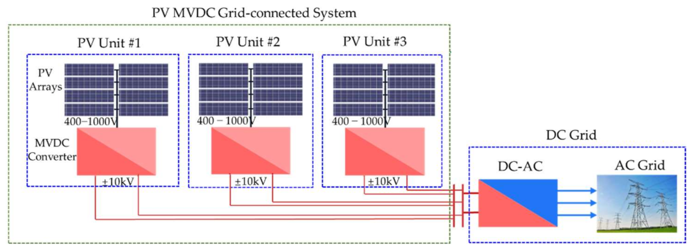
Figure 2.
Topology of the proposed MVDC converter.
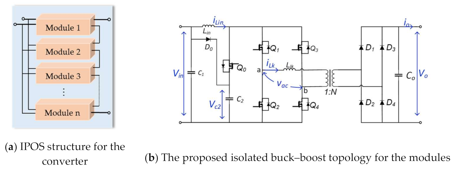
Figure 3.
Equivalent circuit of the proposed isolated buck–boost topology.
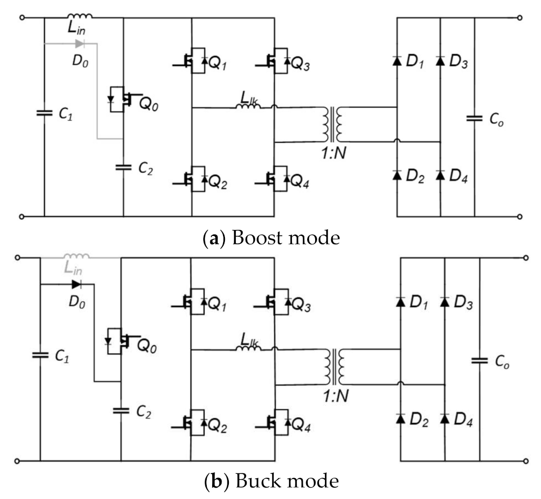
Figure 4.
Switching sequence diagram in boost and buck modes.
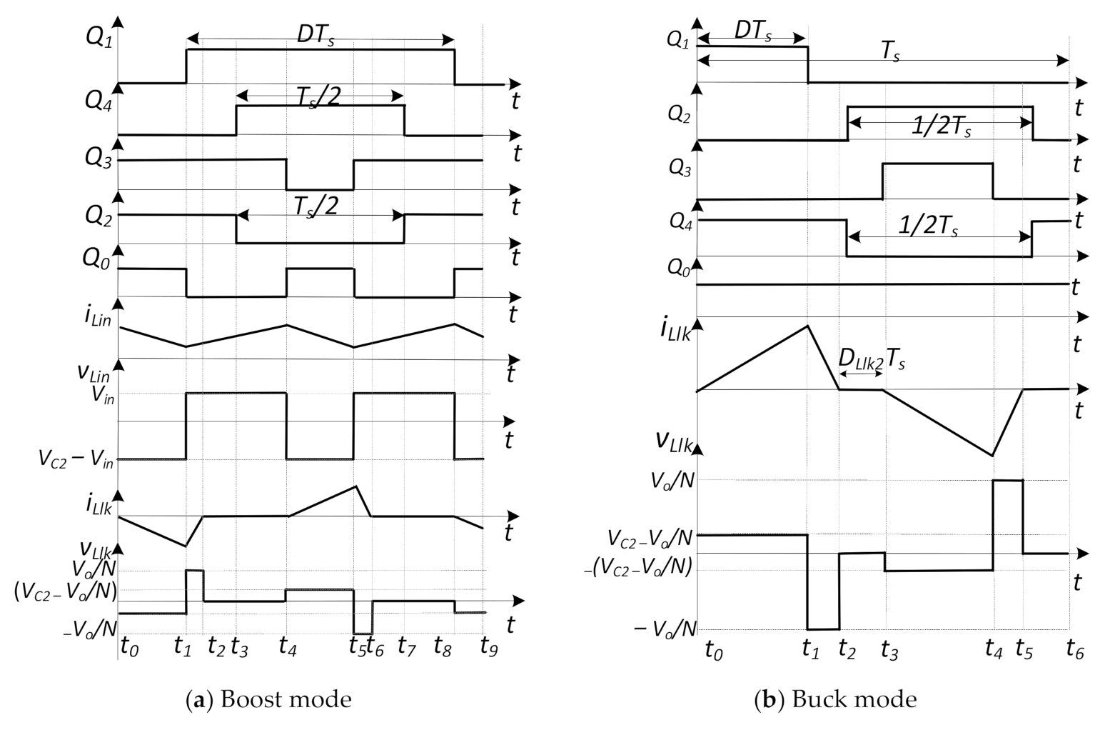
Figure 5.
The relationship between voltage gain and duty cycle.

Figure 6.
Converter topology with LC filter.
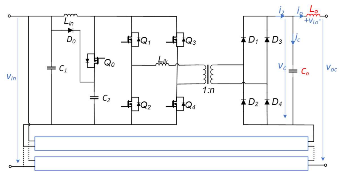
Figure 7.
Circuit of LC and LCR filters.
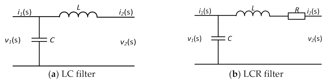
Figure 8.
The bode waveform of LC filter and LCR filter.
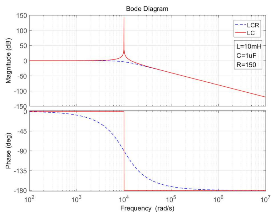
Figure 9.
Model of current closed loop with LC filter.

Figure 10.
Small-signal model in boost mode.
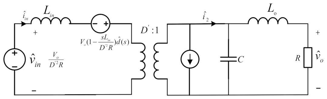
Figure 11.
Small-signal model in buck mode.

Figure 12.
The bode waveform of current loop gain.
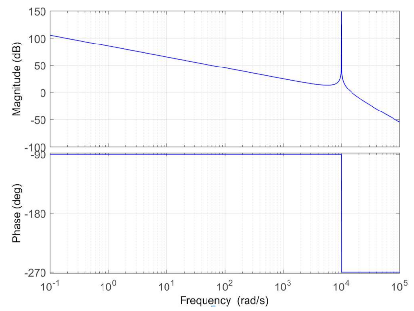
Figure 13.
Block diagram of output current closed-loop control with LCR filter.
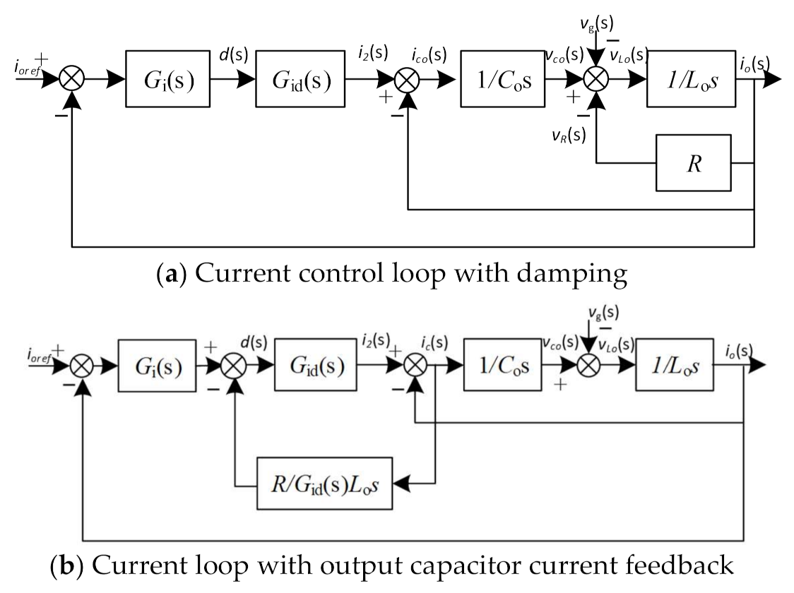
Figure 14.
Equivalent control diagram with output capacitor current feedback.
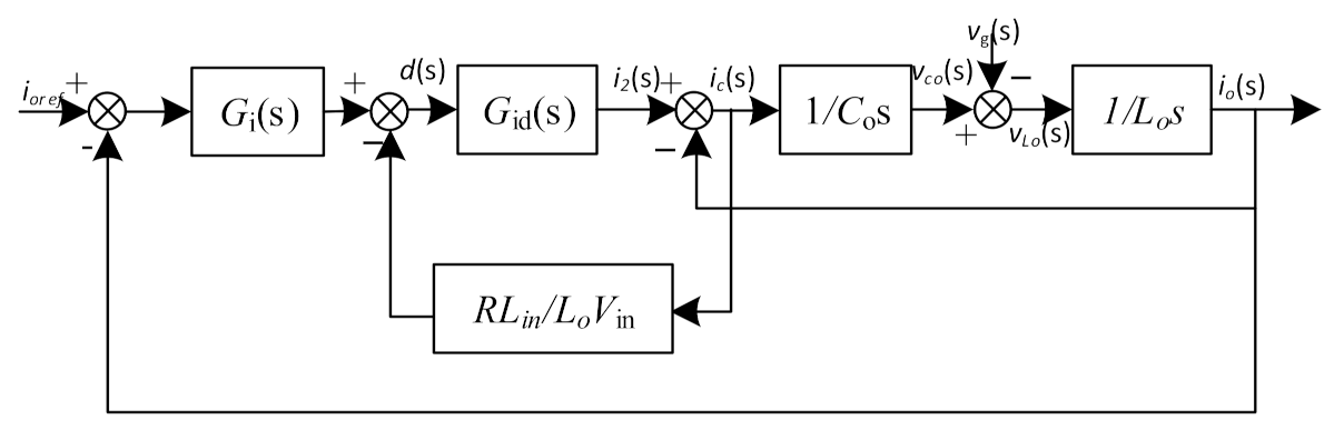
Figure 15.
Loop gain before compensation.
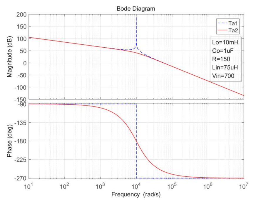
Figure 16.
Loop gain with PI compensation.

Figure 17.
Complete control scheme of the converter.
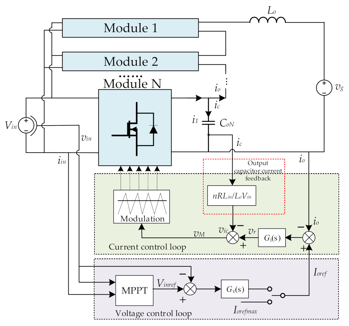
Figure 18.
5 kV/50 kW SiC dc–dc module.
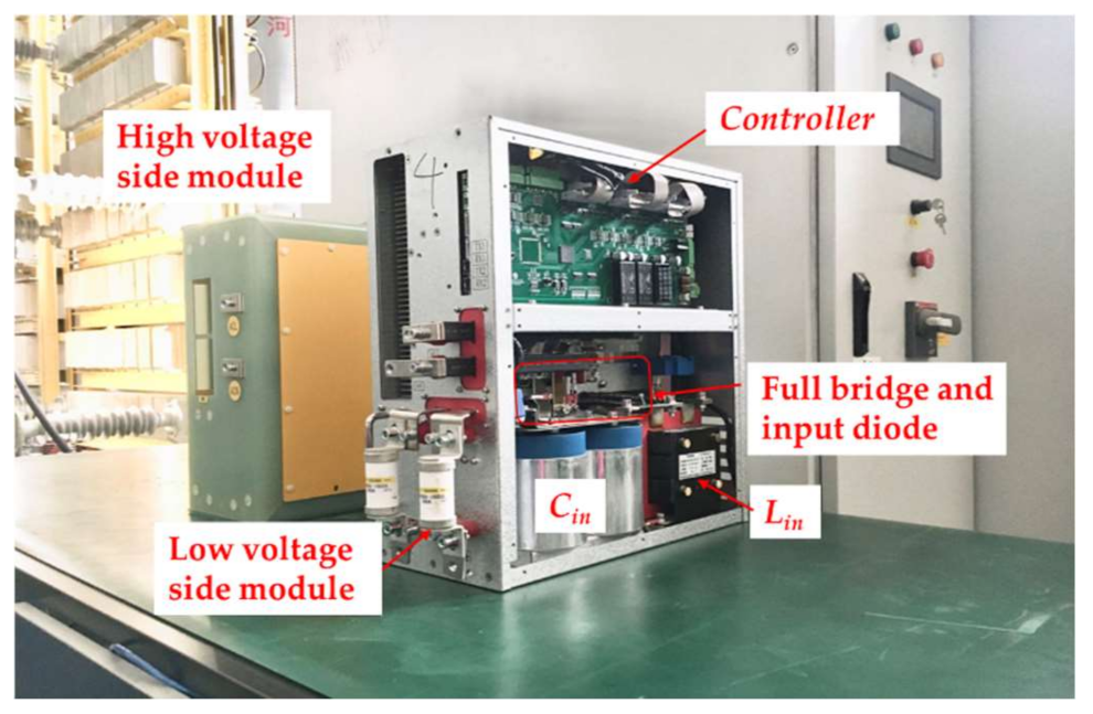
Figure 19.
±10 kV/200 kW SiC PV MVDC converter.
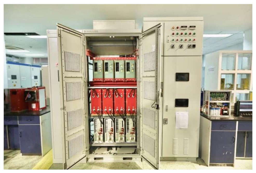
Figure 20.
Experimental waveforms of dc module in two modes.
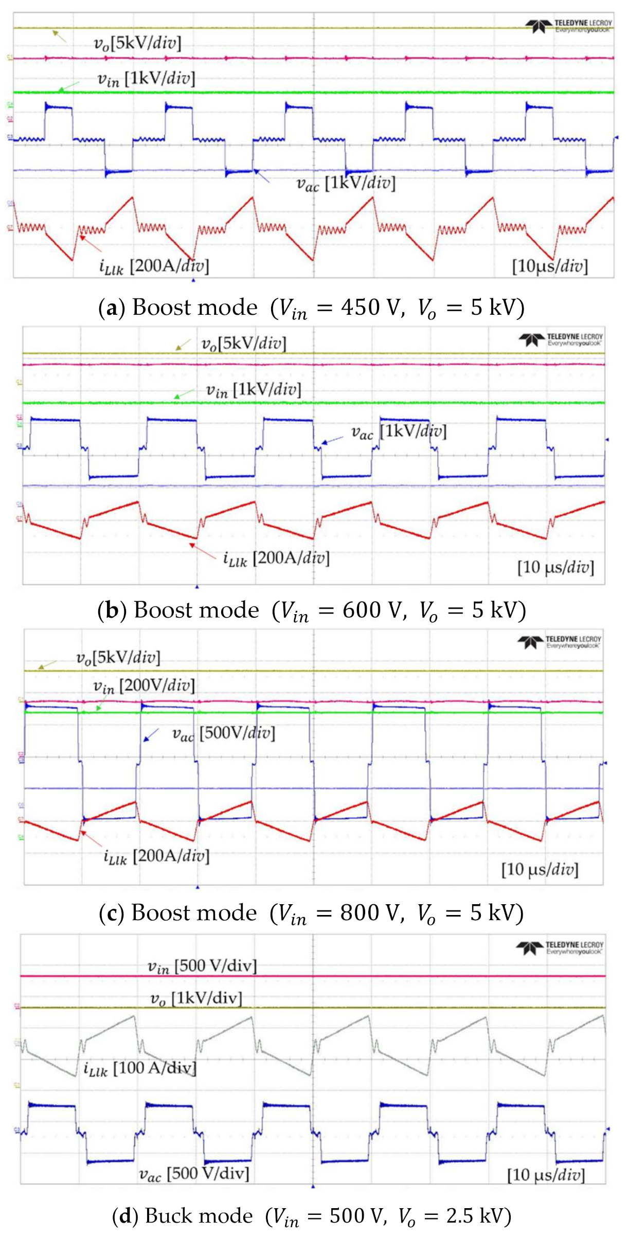
Figure 21.
Measured efficiency of the dc–dc module.

Figure 22.
Voltage gain of the dc–dc module and converter.

Figure 23.
Simulation result of inserting active damping ().
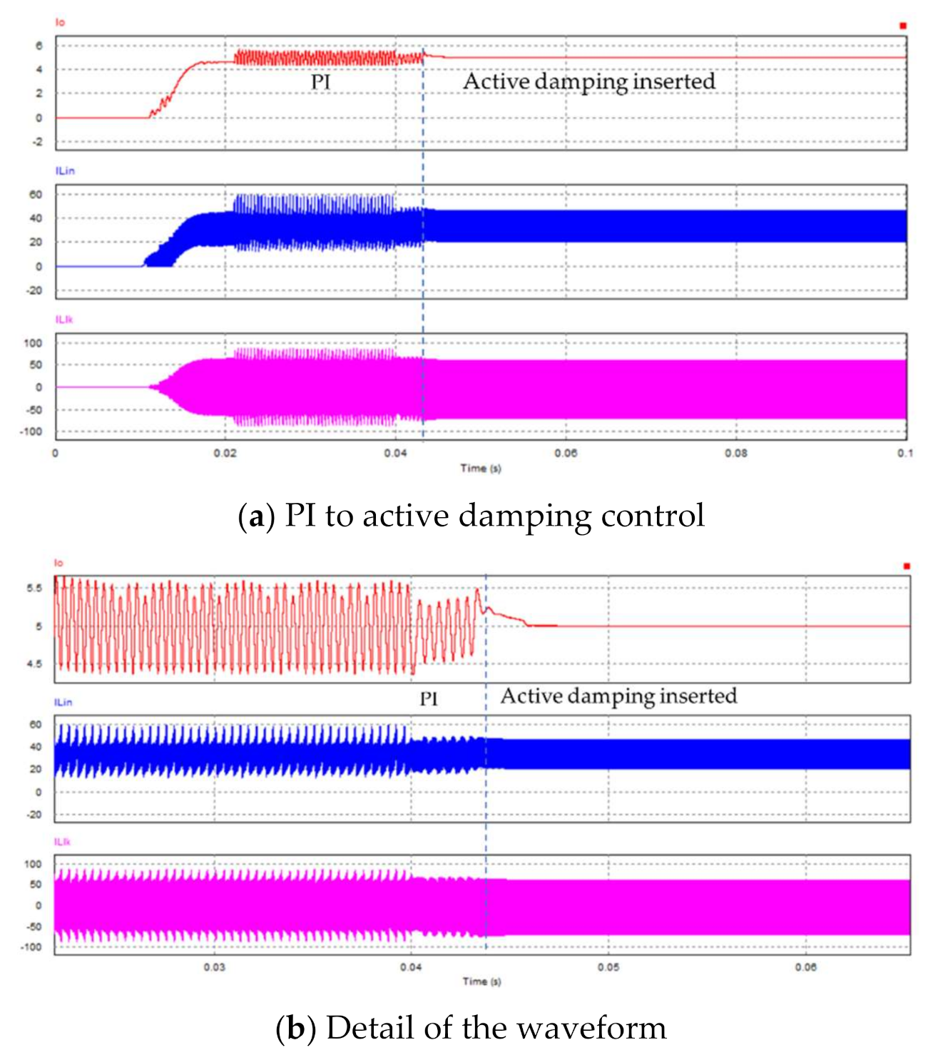
Figure 24.
Simulation result of inserting active damping .
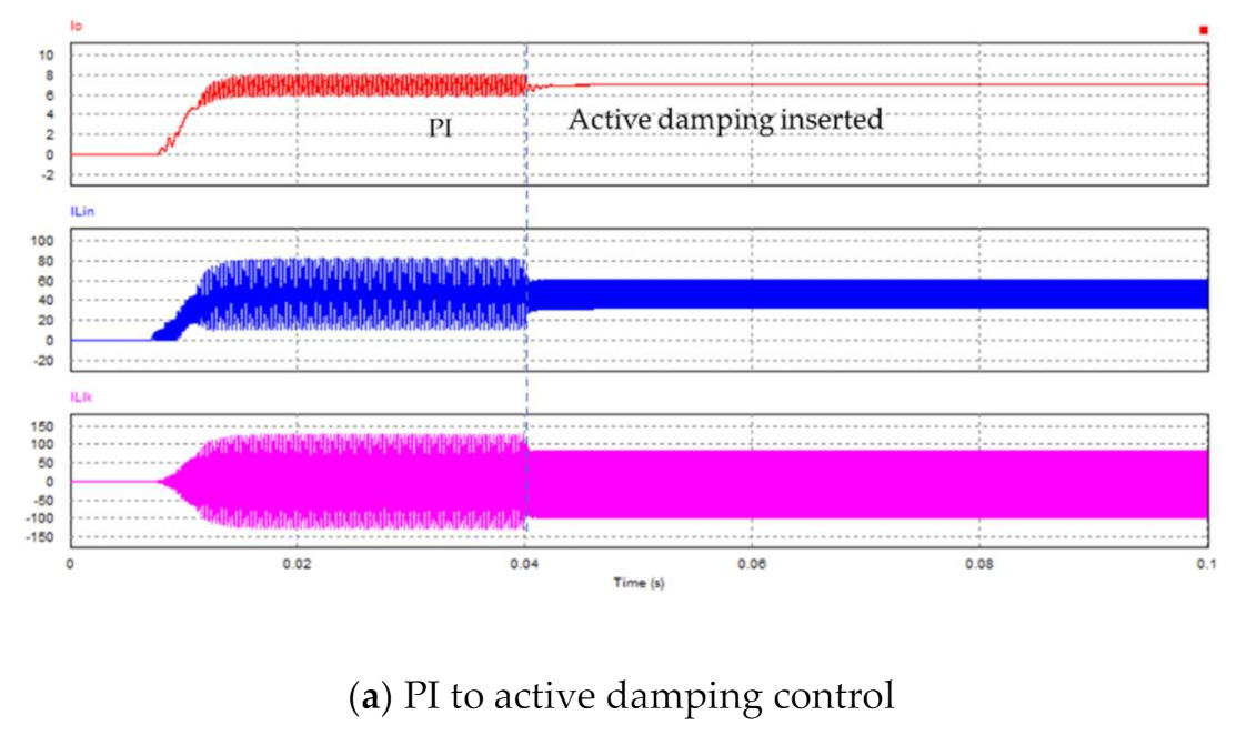
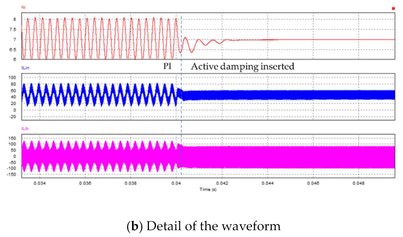
Figure 25.
Experimental result of PI and proposed active damping control.
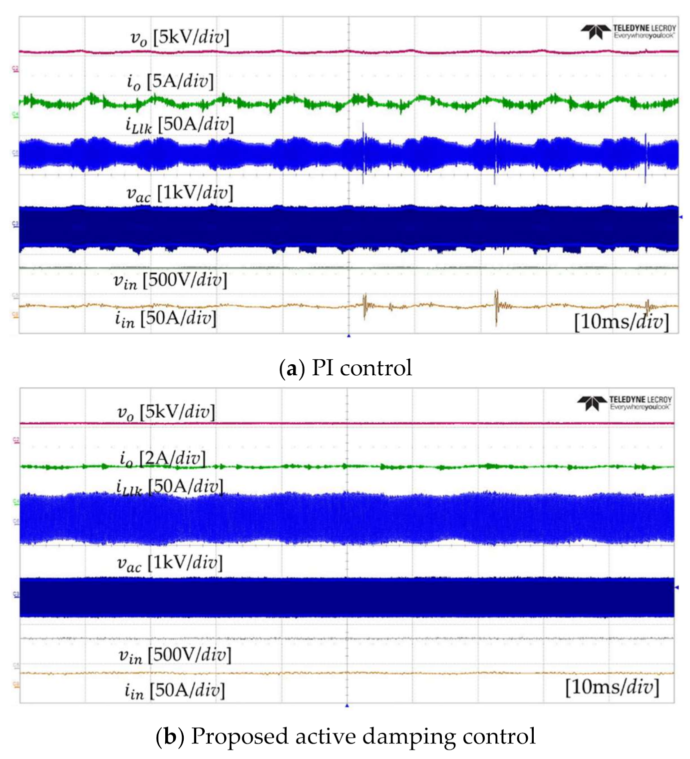
Figure 26.
Experimental result of inserting active damping by proposed method.
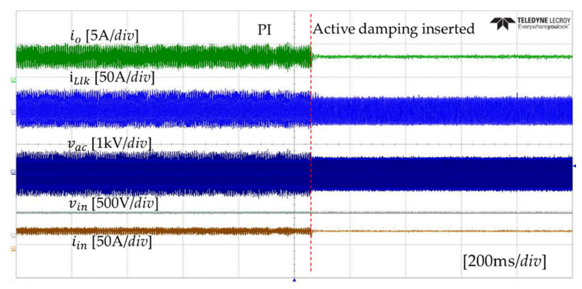
Figure 27.
Simulation result of the process of LVRT.


Figure 28.
Experimental result of the process of LVRT (Grid voltage drops 80%).
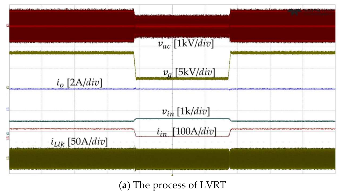

Figure 29.
Experimental result of the process of LVRT (Grid voltage drops 100%).


Table 1.
Voltage gain in boost and buck modes.
| Mode | Voltage Gain | |
|---|---|---|
| Boost | Boost-CCM1 | |
| Boost-CCM2 | ||
| Boost-DCM1 | ||
| Boost-DCM2 | ||
| Buck | Buck-CCM | |
| Buck-DCM1 | ||
| Buck-DCM2 |
Table 2.
Comparison between different isolated topologies.
| Topology | DAB | Isolated Boost | [18] | [20] | Proposed Topology | |
|---|---|---|---|---|---|---|
| High-voltage side | Switches | 4 | 0 | 2 | 2 | 0 |
| Diodes | 0 | 4 | 4 | 2 | 4 | |
| Low-voltage side | Switches | 4 | 5 | 4 | 6 | 5 |
| Diodes | 0 | 0 | 2 | 2 | 1 | |
| Number of capacitors | 2 | 3 | 6 | 4 | 3 | |
| Number of inductors | 0 | 1 | 0 | 0 | 1 | |
| Output voltage | Low | High | Medium | Medium | High | |
| Boosting capability | Low | Strong | Medium | Medium | Strong | |
| Output voltage range | Narrow | Medium | Wide | Wide | Wide | |
| Efficiency | Medium | High | Medium | High | High | |
Table 3.
Parameters of converter and dc module.
| Parameters | Value | |
|---|---|---|
| Converter | Rated output power Pco | 200 kW |
| Rated output voltage Vco | ±10 kV | |
| Input voltage Vin | 450–850 V | |
| Number of modules | 4 | |
| Output inductor Lo | 10 mH | |
| Switching frequency fs | 50 kHz | |
| DC module | Rated power Po | 50 kW |
| Rated output voltage Vo | 5000 V | |
| Output capacitor Co | 1 uF | |
| Input inductor Lin | 75 uH | |
| Transformer ratio N | 5.8 |
Table 4.
Comparison of the output voltage range of different topologies.
| DAB | Isolated Boost | Proposed Topology | |
|---|---|---|---|
| Output voltage range | 0–2.3 kV | 2.3–5 kV | 0–5 kV |
| Input voltage | 400 V | 400 V | 400 V |
| Turn ratio | 5.8 | 5.8 | 5.8 |
Table 5.
Comparison between different control methods.
| PI | Proposed Method | |
|---|---|---|
| Output voltage | 2.5 kV | 2.5 kV |
| Output current | 4 A | 4 A |
| Percent of output current ripple | 30% | 6% |
Publisher’s Note: MDPI stays neutral with regard to jurisdictional claims in published maps and institutional affiliations. |
© 2021 by the authors. Licensee MDPI, Basel, Switzerland. This article is an open access article distributed under the terms and conditions of the Creative Commons Attribution (CC BY) license (http://creativecommons.org/licenses/by/4.0/).
Share and Cite
MDPI and ACS Style
Wang, H.; Zhou, Y.; Huang, X.; Wang, Y.; Xu, H. Topology and Control Strategy of PV MVDC Grid-Connected Converter with LVRT Capability. Appl. Sci. 2021, 11, 2739. https://doi.org/10.3390/app11062739
AMA Style
Wang H, Zhou Y, Huang X, Wang Y, Xu H. Topology and Control Strategy of PV MVDC Grid-Connected Converter with LVRT Capability. Applied Sciences. 2021; 11(6):2739. https://doi.org/10.3390/app11062739
Chicago/Turabian StyleWang, Huan, Yu Zhou, Xinke Huang, Yibo Wang, and Honghua Xu. 2021. "Topology and Control Strategy of PV MVDC Grid-Connected Converter with LVRT Capability" Applied Sciences 11, no. 6: 2739. https://doi.org/10.3390/app11062739
Note that from the first issue of 2016, this journal uses article numbers instead of page numbers. See further details here.