
Diagnosis of Artificial Flaws from Eddy Current Testing Signals Based on Sweep Frequency Non-Destructive Evaluation


Department of Electromagnetic and Biomedical Engineering, University of Zilina, 01026 Zilina, Slovakia
*
Author to whom correspondence should be addressed.
Appl. Sci. 2022, 12(8), 3732; https://doi.org/10.3390/app12083732
Submission received: 11 March 2022
/
Revised: 4 April 2022
/
Accepted: 5 April 2022
/
Published: 7 April 2022
(This article belongs to the Collection Nondestructive Testing (NDT))
Abstract
:An investigation of artificial flaws in electromagnetic non-destructive evaluation using eddy-current frequency-response analysis is carried out in this study. A new approach incorporating innovative solution is proposed. The goal was to increase the resolution of gained signals in contrast to the conventional sweep-frequency method. The proposed procedure was tested on real material specimens where differential responses were gained from artificial electro-discharge machined flaws. Two plate specimens having EDM flaws of various dimensions were inspected. Eddy-current responses due to the material flaws were sensed and compared to a dataset that was obtained by numerical modelling. The presented unique results clearly show that the resolution of a fixed probe driven with sweep-frequency excitation signal can be increased when the appropriate probe instrumentation is used and the characteristics are further mathematically processed.
1. Introduction
Non-destructive testing applications for conductive materials such as material inspection for coating and thickness, conductivity measurements for material identification, heat damage detection, heat treatment monitoring, defect detection, etc., may utilize the eddy current testing (ECT) of available non-destructive methods.
According to Willcox et al., the ability to explore a wide range of properties of conductive materials, as indicated above, is one of ECT’s advantages over other regularly used NDT methods such as ultrasonography, radiography, and magnetic particle inspection. This procedure can also be fully automated, and there are no consumables involved in the investigation. This approach also allows for the use of a variety of probes and test frequencies, allowing for greater versatility in various applications. There isn’t a required high level of detection capability there, unlike in ultrasonography. Yet, ECT and ultrasonography share the same favourable quality. The automated system can quickly determine if a test result is positive or negative. The effect of varying material parameters other than the presence of a defect is the method’s worst shortcoming, which is also its major gain [1].
ECT methods use various exciting signals, i.e., single-frequency, multiple-frequency, sweep-frequency, and pulsed or transient signals. The sweep-frequency eddy current (SFECT) techniques are based on the measurement of eddy current data at a wide range of frequencies. The SFECT technique can be a difficult and time-consuming measurement, however, it provides the advantage of obtaining depth information. This information is acquired since the eddy current depth of penetration varies as a function of frequency.
It has been empirically proven that the multifrequency ECT approach improves the signal-to-noise ratio by up to 1100%, according to Garcia-Martin [2].
The widely used implementation of SFECT is for layer inspection. The application is broad; it may be used for the simultaneous measurement of the coating thickness even for nonconductive materials, coating conductivity, substrate conductivity, etc. According to Xu et al., the goal of conductivity evaluation may be achieved by analogizing eddy current testing to the parameter measurement process using the apparent conductivity. In their study, the authors evaluate both coil impedance and plane wave impedance, and the approximation relationship between them. They found that all properties of the coated plate may be determined by comparing the experimental curve of the experimentally gained equivalent conductivity of coil impedance with the theoretical curves of normalized apparent conductivity of plane wave impedance [3,4,5].
According to Xu et al., the variations due to lift-off in coil impedance measured with the coil positioned above a conductive plate with and without a thin metallic coating can be utilized for the simultaneous assessment of the thickness and conductivity of metallic coatings. The lift-off effect was eliminated using an impedance coordinate transformation approach. The impedance of the coil placed above the plate under test was normalized by the impedance of the coil placed above two reference plates. The suggested technique, which combines the least-squares method with the Levenberg–Marquardt (LM) algorithm, may be used to determine the parameters of a multilayer metallic coating with a thickness of tens of micrometers on a conductive plate [6,7].
When characterizing the multi-layered structure, the signals of the to-be-characterized layer are ‘extracted’ from the composite signals. Cheng et al. proposed the method of separating the signals of different layers by frequency band and characterizing the layer of interest by using the correspondent signals. The study of the simulated signals and the differences of the signal series in the frequency series yielded a few distinguishing parameters. The thickness of the top and bottom layers may be measured using high-frequency and low-frequency signals, respectively. The air gap between two conductive layers does not affect the variations in the signal series in the frequency series. They stated that even without knowing the plate’s conductivity, the maximum difference in resistance in the frequency series can be used to characterize the lower layer regardless of conductivity changes and air gaps [8,9,10].
The impedance signal is an integrand of the form function and generalized reflection function when using SFECT to evaluate each layer’s thickness in a layered construction. Cheng et al. presented the variable—a derivative of impedance concerning log scaled angular frequency to assess two closely linked layers. Spectral analysis of impedance or frequency derivative related quantities, such as extrema of the real or imaginary parts of the variable, suggested that the top layer’s thickness could be determined using characteristic features taken from high-frequency signals, and the lower layer’s thickness could be determined later using characteristic features taken from lower frequency signals [11,12].
Chen et al. also proposed a hybrid serial/parallel multi-frequency measurement method for measuring the impedance/inductance of eddy current sensors. They proposed a combination of parallel multi-frequency measurement which has a higher measurement speed but a lower signal-to-noise ratio, and the serial multi-frequency (sweeping frequency), which has a lower measurement speed but a higher signal-to-noise ratio. The proposed method allows for the flexible combination of these two features to deliver the desired speed and SNR according to the requirements of a specific application [13,14,15,16,17].
Stubendekova et al. conducted measurements utilizing SFECT on a plate specimen of austenitic steel AISI 316L with artificial electro-discharge machined notches probed by two eddy current probes. The study was conducted over a wide frequency range, with the probes comprising transmitting and receiving coils set in a fixed place. The effect of the defect length on the response signals was assessed to study the method’s resolution. Results showed that the resolution between the response signals of defects of various lengths allows for the detection of defects, however, the resolution between the response signals is only possible up to a certain defect length, which is related to inspection probe dimensions [12].
Further study of crack geometry influence on transmission frequency characteristics experimentally studied by Janousek et al. was focused on various lengths and depths of artificial notches. The presented results clearly show that the frequency transfer functions depend on the defect’s dimensions [18,19].
This paper deals with SFECT numerical and experimental inspection of various flaws differing in geometry. Two AISI316L plates are inspected using a transmitter–receiver eddy-current probe in three different configurations. The plates contain electro-discharge machined surface flaws of the cuboid shape. At the first plate, only the length dimension of notches is varied, whereas the second plate contains flaws with different depths, keeping other dimensions the same. The flaws are numerically modelled and experimentally inspected. During the inspection of each flaw, the probe is fixed over the center of that flaw and the frequency of the exciting signal is changed in a wide range while response signals are sensed. The frequency range is selected to cover the range from low to high frequencies. The response signals for each particular flaw are further processed in order to investigate the differences between the signals for flaws obtained numerically and experimentally. The presented results report positive findings and the paper thus brings a new perspective on the possibilities of non-destructive evaluation of flaws from SFECT signals.
This paper is organized as follows, as shown in Figure 1. The numerical model of the studied plates and sensors, as well as the simulation results, are briefly described in Section 2–line 1 progress in Figure 1. Section 3 describes the experimental setup and experiments–line 2 progress in Figure 1. Section 4 contains the experimental data and comments. Section 5 brings conclusions with a summary of the findings.
2. Numerical Simulation Procedure
The numerical modelling approach is used mainly to reduce the necessary time for a further experimental investigation. It can be used to investigate materials with various parameters, whether geometric or electromagnetic. The results can only be taken into account if they are subsequently verified by the measurements, with an appropriate match in the results. Numerical simulations in this work are performed using the CST Studio Suite software process of modelling the interaction of the electromagnetic field with the conductive structure. The software uses the finite element method (FEM) for the calculation and analysis itself.
The eddy-current probes that were used during the numerical investigation are presented, and their parameters summarized, in Table 1.
Each of the new SFECT probes consists of a two-coil system. The first coil serves as a transmitter (Tx), hence as a generator of the electromagnetic field. The second coil is used to pick up the response signal and is named a receiver (Rx). The cross-section of the probes is shown in Figure 2.
For simulation and experimental purposes, we utilized a conductive plate specimen with a thickness of hs = 10 mm, a width of ws = 150 mm, and a length of ls = 500 mm; the electromagnetic parameters of the stainless steel AISI 316L (chromium-nickel-molybdenum steel with a carbon content of up to 0.03%, acid and corrosion-resistant, with a little susceptibility to pitting corrosion in chloride-containing solutions) were inspected in this study. The material has the conductivity of σ = 1.4 MS/m and the relative permeability of μr = 1. The value of the lift-off parameter is set to lift-off = 0.5 mm. This value was also used in the implementation of the experiments and was given by the construction of the measuring probes. There were no changes in the lift-off parameter during the simulations and experiments.
Each specimen contained five non-conductive defects and were rectangular in shape, as shown in Figure 3. Five artificial flaws were present in each specimen. The flaws were rectangular in shape and their dimensions varied for each specimen: specimen No. 1 contained five defects with different depths. The depths were in the range of dsp1 = <1 mm; 9 mm>, with 2 mm step. Specimen No. 2 contained five flaws of varying lengths: lsp2 = <10 mm; 30 mm> with 5 mm step. The geometry of all flaws are listed in Table 2.
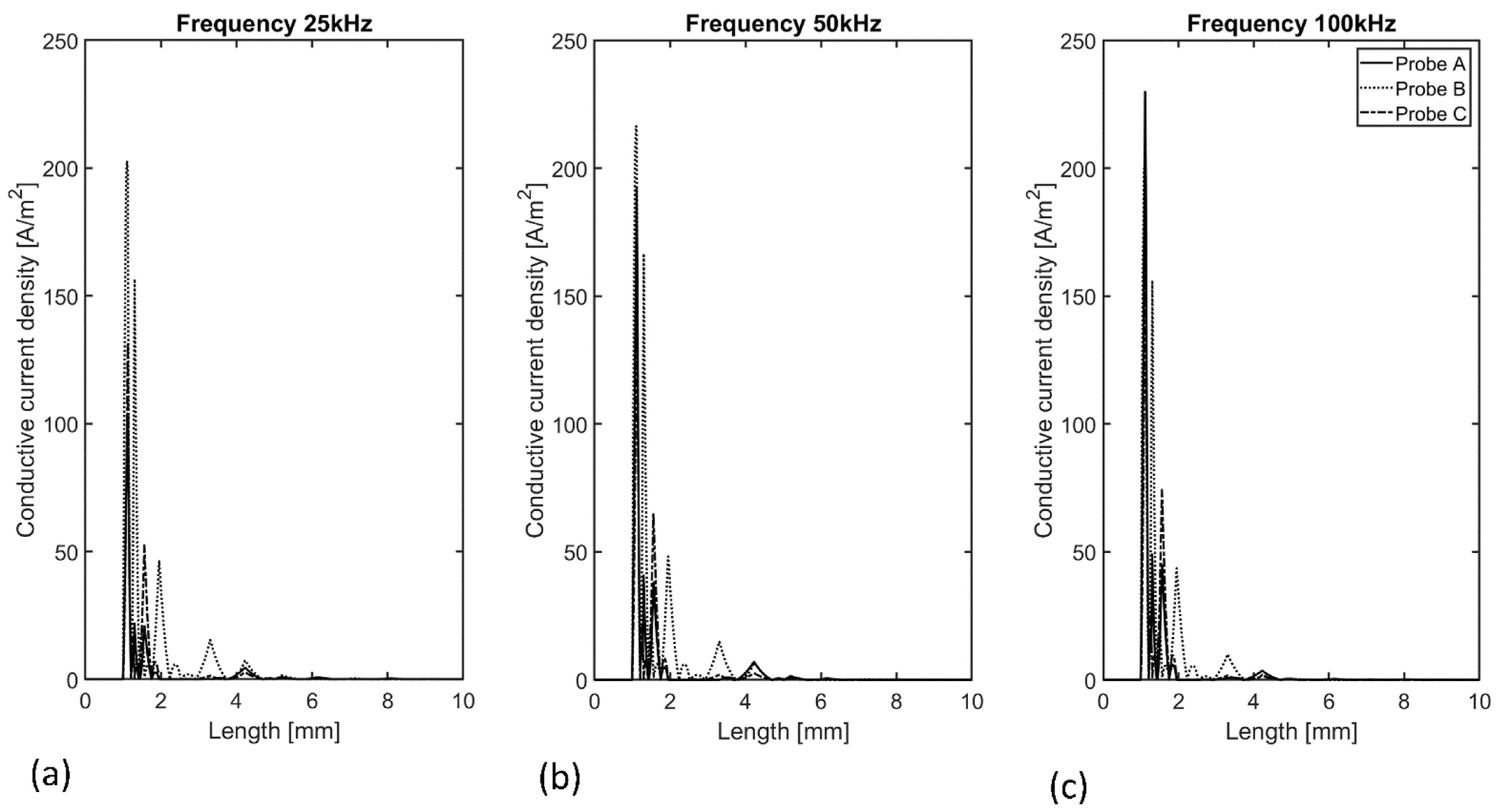
After performing each numerical simulation, the values of the magnetic induction in the whole volume of the receiving coil were extracted, then integrated and subsequently converted into the values of the voltage of the pick-up coil. These values from each simulation are used for further processing, based on the presented algorithm. More than 7.5k simulations were performed, and the methods of adaptive-mesh refinement were used to reduce the computational time. Figure 4, Figure 5 and Figure 6 show the results for each simulated probe, where the probe is in the static position, and the frequency of the excitation signal is changing in discrete steps. A color map in the form of redistribution of the current density field is displayed.
The values obtained from the simulations were directly used for further processing, where they were decomposed into real and imaginary parts of the coil impedance. From these values, it is possible to calculate the frequency response of the material to the excitation signal as well as the effect of the presence of the flaw. All necessary math calculations and operations were performed by Matlab software. The values obtained from the air-core coil simulation were used as reference values, which were subtracted from the material simulation values. The results were then normalized to the reference value. The complex impedance of the coil is normalized by the complex impedance of the coil in the air according to the formula:
where ΔVnorm [V] is the normalized value of the voltage of the coil, ΔVsim [V] is the difference between the coil voltage in the air and from the simulation, Vsim [V] is the voltage of the coil in the presence of the material and Vair [V] is the voltage of the coil in the air. The normalized coil voltage module is calculated using the following formulas:
Based on these findings and used parameters, identical probes were manufactured for experimental verification and measurements.
Figure 7 displays the results for individual frequencies, where the probe is in the static position, and the length of the defect is changing.
3. Experimental Setup: A New Approach
All the measurements were performed using identical measuring probes and plate specimens used in the numerical simulations. The measuring apparatus contains individual measuring components that are necessary for generating, sensing, filtering, processing, and visualizing the measured signals. The measurements were performed on both conductive specimens with EDM notches, respectively. The dimensions of all defects were precisely defined by the vendor and re-measured using (electromagnetic-acoustic-transducer-method) EMAT and RT (radiography testing) methods.
In essence, the following instruments were required to perform the measurement using the sweep-frequency eddy-current method: the material under investigation, the new SFECT probe, lock-in amplifier (Signal Recovery DSP 7280), a PC (personal computer) with the LabVIEW platform and DAQ card (National Instruments, Austin, TX, USA).
The probe (air-core) consisted of two coils with an air-core. The measured value of the self-inductance of the coil Rx was LRx1 = 4.7 μH, and the inductance of the Tx coil was LTx1 = 11 μH. The probe (ferromagnetic-core) had the same dimensions as the previous one, it differed only in the presence of a ferromagnetic core, and the value of inductances were as follows: LRx2 = 25 μH and LTx2 = 64 μH. The third probe (ferromagnetic-core and metal shielding) was of the same dimensions as the previous ones with the additional aluminum shielding; it had the following parameters: LRx3 = 33 μH and LTx3 = 55 μH, Figure 8.
The transmitting coil was supplied by an alternating harmonic signal (voltage) generated by the 7280 DSP Lock-in amplifier (Figure 9). The signal’s magnitude was VPP = 0.1 V. The generated harmonic signal had a frequency range of fg = <1 kHz; 1400 kHz>. It varied in fstep = 5 kHz steps, with a sweeping time of tsweep = 2 s for each frequency. A lock-in amplifier that simultaneously served as a data-filtering device was used to measure the induced voltage of the receiving coil. Each material defect was examined for each plate by three probes. In this approach, the probe, in a static position, was used without any movement above the inspected material. Three probe locations were used in the numerical simulation as well as for whole measurements: probe in the air (case A), probe above the defect-free material as a reference (case B), and probe axially symmetrically above the material with the defect (case C).
Data storage in the form of two separate data files was realized with the use of LabVIEW software. The data containing the real part of the induced voltage were saved separately in one file, and the data for the imaginary part were in another file. The program read s =1000 samples from the lock-in amplifier with a sampling frequency of fs = 10 kHz. The average value was then calculated and saved in the file using these datasets.
4. Results and Discussions
Ten EDM flaws introduced in two AISI 316L plate specimens were inspected using the SFECT probes according to the explanation provided in the previous section. Figure 10, Figure 11 and Figure 12 present the obtained results from two different points of view: the data are displayed in the form of magnitude on frequency dependences as well as phase on magnitude dependences, respectively. The goal is to show the differences that are contained on the appropriate sets of signals, based on the different data-processing and displaying methods. The figures show that the resolution between individual signals strongly depends on the type of probe used and inspected flaws. It can be seen that the inspections performed with probes A and B bring unambiguous information about the presence of a flaw in the inspected specimen, and it is easy to visually distinguish this signal from others.
On the other hand, individual flaws’ signals were not sufficiently separated. This deficiency is relatively suppressed in the waveforms obtained with probe C. Basically, the effective frequency interval of the used probes is at the level of tens of kHz.
The next three figures (Figure 13, Figure 14 and Figure 15) present the situation for specimen No. 2, where the length of flaws varies. In this examination, the following conclusions can be stated: when using probes A and B, the signal-to-signal ratio of the signal without defect to the other signals is the most obvious. By using a probe with a ferromagnetic core and a shielding metal cover, the resolution between the individual defect signals was increased. It can be concluded that when using a presented innovative approach using the sweep-frequency eddy-current method (in comparison with the conventional approach), it is possible to extract useful information about the flaw. Following the scanning and signal-processing procedure is necessary. The purpose of using separate sensing and appropriate processing is that such an innovative approach can increase the resolution of the method without the need to further increase the sensitivity of the individual components of the measuring apparatus.
For the comparison and determination of the degree of correlation between the results of the numerical simulations and performed experiments, the following procedure was used: values of the induced voltage of the Rx coil were acquired and processed from the simulations and measurements. In the simulations, the values of the induced voltage for individual frequencies were obtained from the overall results of each simulation. During measurements, the data processing was more complex. The gained eddy-current signal was in the form of the real and imaginary part of the induced voltage and these are the averaged values from the whole samples. MATLAB software was used to connect these parts to become magnitude and phase values. The induced voltage values VRx were mathematically adjusted. The results of the induced voltage VRx in the air were subtracted from the other results for the obtained signal to accurately depict the material’s response to the excitation signal. The response to the Tx coil was thus eliminated. The data were then normalized to the absolute value of the probe voltage in the air using the following equation:
where, VRx [-] is the normalized voltage, VRx-defect [V] is the voltage of the coil over the defect or defect-free material, and VRx-air [V] is the voltage of the coil in the air. After normalization, the magnitude and phase of the normalized induced voltage were calculated. These values were next used for waveform construction with the purpose of comparing simulated and measured data. Therefore, the set of results was further statistically analyzed. First, the individual results of the measurement were subtracted from the corresponding results of the simulations, according to the equation:
where ΔV [-] is the voltage difference, VRx-simulation [-] is the normalized voltage of the simulated coil, and VRx-measurement [-] is the normalized voltage of the measured coil. The difference ΔV between the two values was plotted and evaluated. The difference was plotted by three graphs for each probe.
Figure 16 clearly shows that the largest differences between the resulting values obtained from the numerical simulations and experiments are observable for probes B and C. The degree of this uncertainty, on the other hand, is compensated by the better resolution of these probes, especially when detecting deeper defects (especially with the depth of 7 mm and 9 mm). The measurement results of the A probe and the B probe are more accurate than the C probe. The strongest difference was found around the frequency interval’s edges, particularly at lower frequencies. The same oscillation that occurred in the measurement results of probe A was responsible for the oscillation.
Furthermore, the addition of the aluminum shielding had a different effect on detection than the simulation predicted. Despite having the widest difference between the simulated and measured data, probe C presented sufficient detection ability.
Table 3 presents the previous information through the prism of selected statistical parameters. This analysis was performed to better evaluate the results. For each statistical file, the median and standard deviation were calculated. The statistical set represented the results of individual coil geometry change differences. The consistency of the differences is described by these results. The results show that despite the initial oscillation of the waveform probe A performs the best results. The average difference in probe B is slightly higher. The results that are still relatively sufficient were obtained by probe C: the standard deviation is 12–14 times higher when compared to probe A.
5. Conclusions
This paper focused on SFECT and the improvement of the flaw-response signal’s resolution by a fixed probe. A new eddy-current probe containing galvanically isolated excitation and receiving electromagnetic system with different configurations was designed for this study. Two conductive austenitic steel specimens were inspected by numerical as well as experimental means by the three probes. There were five artificial EDM flaws of cuboid shape in each plate differing in depth or length dimensions. Each eddy-current probe was fixed in a given position to a given flaw during the inspection. The excitation frequency of the individual probes was changed in a defined interval <1 kHz; 1400 kHz> with a given discrete frequency step of 5 kHz. The frequency response signals were measured and processed to give higher information content in terms of better resolution among individually measured signals. The presented results showed that the geometry of the flaw strongly affects differential response through its magnitude and phase, and there exists a correlation between the defect geometry and signal frequency response. It was also discovered that even for the frequency range in the order of hundreds of kHz, deeper flaws are still clearly distinguished from each other based on the individual signals. The presented method of inspection of conductive structures using the SFECT method can be applied in two different approaches in real conditions: in the first approach, the SFECT method can be used after the previous investigation using the conventional ECT method; in the second approach, it can be used without previous investigation. In this case, the measuring probe must be placed directly where defects are expected to occur. This important information opens a new view into the possible utilization of the SFECT with fixed probes in the electromagnetic non-destructive evaluation of defects.
Author Contributions
Conceptualization, M.S., D.G. and F.V.; methodology, M.S., F.V. and D.G.; software, F.V.; validation, M.S. and D.G.; formal analysis, M.S. and F.V.; investigation, F.V.; resources F.V. and L.J.; data curation, M.S.; Writing—original draft preparation, M.S. and D.G.; writing—review and editing, M.S. and D.G.; visualization, F.V. All authors have read and agreed to the published version of the manuscript.
Funding
This research received funding by the Slovak Research and Development Agency (contract number APVV-19-0214).
Institutional Review Board Statement
Not applicable.
Informed Consent Statement
Not applicable.
Data Availability Statement
Not applicable.
Conflicts of Interest
The authors declare no conflict of interest.
References
- Willcox, M.; Downes, G. A Brief Description of NDT Techniques; Insight NDT Equipment Ltd.: Herefordshire, UK, 2003. [Google Scholar]
- Garcia-Martin, J.; Gómez-Gil, J.; Vázquez-Sánchez, E. Non-Destructive Techniques Based on Eddy Current Testing. Sensors 2011, 11, 2525–2565. [Google Scholar] [CrossRef] [PubMed] [Green Version]
- Xu, J.; Wu, J.; Wan, B.; Xin, W.; Ge, Z. A novel approach for metallic coating detection through analogizing between coil impedance and plane wave impedance. NDT E Int. 2020, 116, 102308. [Google Scholar] [CrossRef]
- Janousek, L.; Smetana, M.; Capova, K. Enhancing information level in eddy-current non-destructive inspection. Int. J. Appl. Electromagn. Mech. 2010, 33, 1149–1155. [Google Scholar] [CrossRef]
- Rebican, M.; Chen, Z.; Yusa, N.; Janousek, L.; Miya, K. Shape reconstruction of multiple cracks from ECT signals by means of a stochastic method. IEEE Trans. Magn. 2006, 42, 1079–1082. [Google Scholar] [CrossRef]
- Xu, J.; Wu, J.; Xin, W.; Ge, Z. Measuring Ultrathin Metallic Coating Properties Using Swept-Frequency Eddy-Current Technique. IEEE Trans. Instrum. Meas. 2020, 69, 5772–5781. [Google Scholar] [CrossRef]
- Li, Y.; Tian, G.Y.; Simm, A. Fast analytical modelling for pulsed eddy current evaluation. NDT E Int. 2008, 41, 477–483. [Google Scholar] [CrossRef]
- Cheng, W.; Hashizume, H. Characterization of multilayered structures by swept-frequency eddy current testing. AIP Adv. 2019, 9, 035009. [Google Scholar] [CrossRef] [Green Version]
- Xin, J.; Lei, N.; Udpa, L.; Udpa, S.S. Rotating field eddy current probe with bobbin pickup coil for steam generator tubes inspection. NDT E Int. 2013, 54, 45–55. [Google Scholar] [CrossRef]
- Kim, D.; Udpa, L.; Udpa, S. Remote field eddy current testing for detection of stress corrosion cracks in gas transmission pipelines. Mater. Lett. 2004, 58, 2102–2104. [Google Scholar] [CrossRef]
- Cheng, W.; Hashizume, H. Determination of Layers’ Thicknesses by Spectral Analysis of Swept-Frequency Measurement Signals. IEEE Sens. J. 2020, 20, 8643–8655. [Google Scholar] [CrossRef]
- Stubendekova, A.; Janousek, L. Non-destructive testing of conductive material by eddy current air probe based on swept frequency. J. Elect. Eng. 2015, 66, 174–177. [Google Scholar] [CrossRef] [Green Version]
- Chen, Z.; Salas-Avlia, J.R.; Tao, Y.; Yin, W.; Zhao, Q.; Zhang, Z. A novel hybrid serial/parallel multi-frequency measurement method for impedance analysis in eddy current testing. Rev. Sci. Instrum. 2020, 91, 024703. [Google Scholar] [CrossRef] [PubMed]
- Rubinacci, G.; Tamburrino, A.; Ventre, S. Fast numerical techniques for electromagnetic nondestructive evaluation. Nondestr. Test. Eval. 2009, 24, 165–194. [Google Scholar] [CrossRef]
- Mao, X.; Leib, Y. Thickness measurement of metal pipe using swept-frequency eddy current testing. NDT E Int. 2016, 78, 10–19. [Google Scholar] [CrossRef]
- Jardine, A.K.S.; Lin, D.; Banjevic, D. A review on machinery diagnostics and prognostics implementing condition-based maintenance. Mech. Syst. Signal Process. 2006, 20, 1483–1510. [Google Scholar] [CrossRef]
- Balageas, D.; Fritzen, C.P.; Guemes, A. Structural Health Monitoring, 1st ed.; ISTE Ltd.: London, UK, 2006; ISBN 1-905209-01-0. [Google Scholar]
- Vaverka, F.; Smetana, M.; Gombarska, D.; Janousek, L. Nondestructive Evaluation of Conductive Biomaterials Using SFECT Method. Measurement 2021. In Proceedings of the 13th International Conference, Smolenice, Slovakia, 17–19 May 2021. [Google Scholar]
- Michniakova, M.; Janousek, L.; Smetana, M. Impact of probe configuration on cracks depth resolution in pulsed eddy current non-destructive evaluation. Electr. Rev. 2012, 88, 226–228. [Google Scholar]
Figure 1.
Algorithmizing of actions: the procedure used to conduct this study.
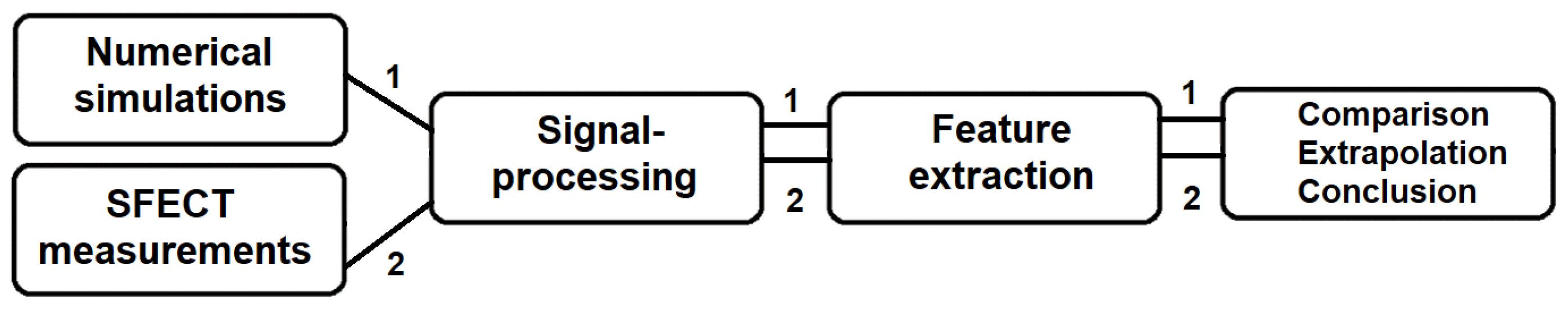
Figure 2.
Cross-section and geometry of SFECT probes: (A) air-core probe, (B) probe with ferrite core, (C) probe with ferrite core and aluminum shield.
Figure 2.
Cross-section and geometry of SFECT probes: (A) air-core probe, (B) probe with ferrite core, (C) probe with ferrite core and aluminum shield.

Figure 3.
Spatial configuration of the specimen with presence of artificial flaws (A) and geometry of the flaw (B).
Figure 3.
Spatial configuration of the specimen with presence of artificial flaws (A) and geometry of the flaw (B).
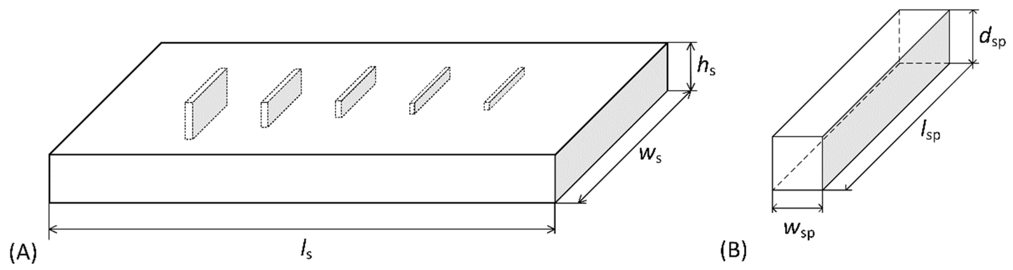
Figure 4.
Numerical simulation: current density module (Conductive current density) distribution within the conductive structure at different excitation frequencies: (a) f = 25 kHz, (b) f = 50 kHz, (c) f = 100 kHz, probe A.
Figure 4.
Numerical simulation: current density module (Conductive current density) distribution within the conductive structure at different excitation frequencies: (a) f = 25 kHz, (b) f = 50 kHz, (c) f = 100 kHz, probe A.
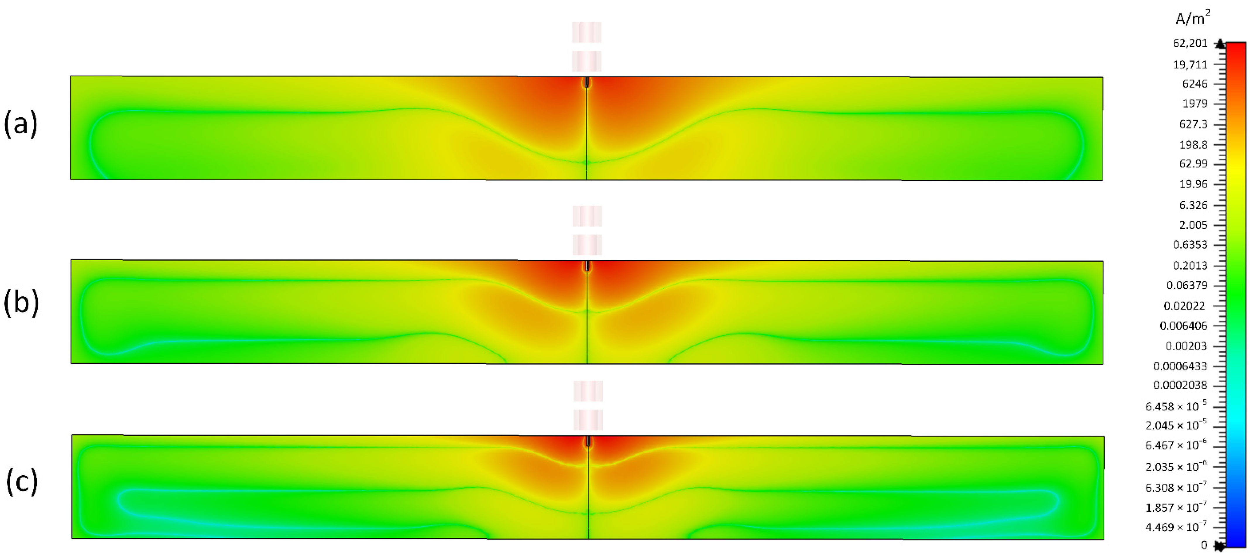
Figure 5.
Numerical simulation: current density module (Conductive current density) distribution within the conductive structure at different excitation frequencies: (a) f = 25 kHz, (b) f = 50 kHz, (c) f = 100 kHz, probe B.
Figure 5.
Numerical simulation: current density module (Conductive current density) distribution within the conductive structure at different excitation frequencies: (a) f = 25 kHz, (b) f = 50 kHz, (c) f = 100 kHz, probe B.
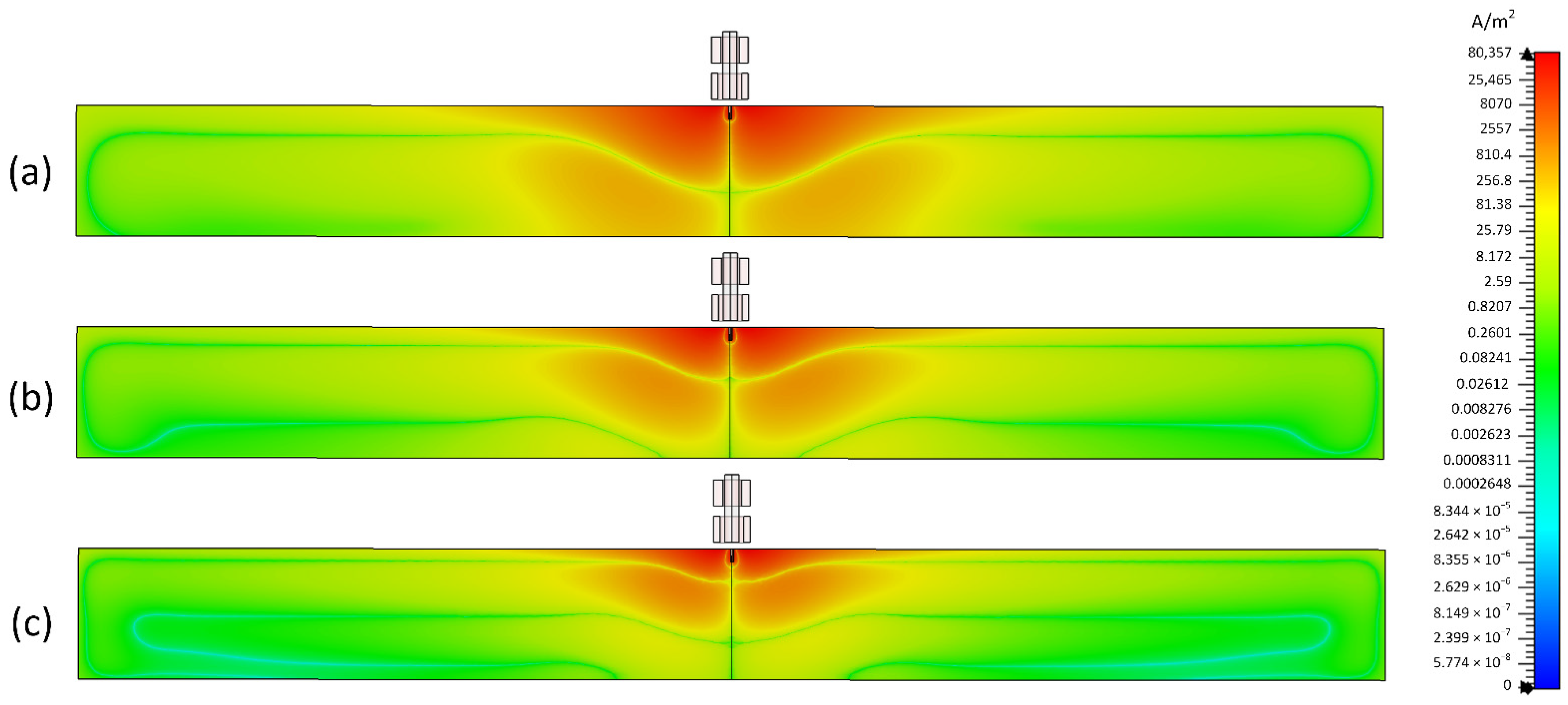
Figure 6.
Numerical simulation: current density module (Conductive current density) distribution within the conductive structure at different excitation frequencies: (a) f = 25 kHz, (b) f = 50 kHz, (c) f = 100 kHz, probe C.
Figure 6.
Numerical simulation: current density module (Conductive current density) distribution within the conductive structure at different excitation frequencies: (a) f = 25 kHz, (b) f = 50 kHz, (c) f = 100 kHz, probe C.
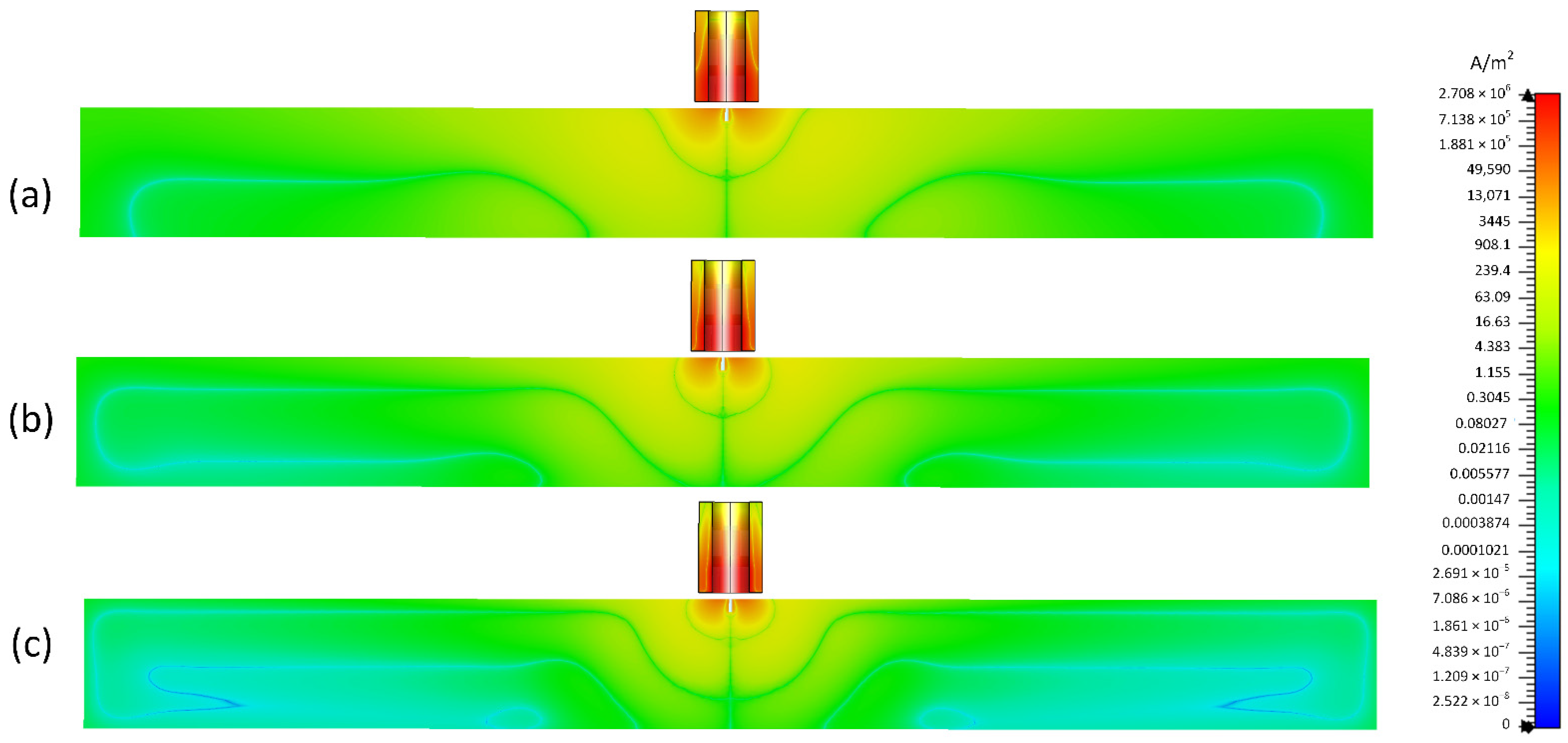
Figure 7.
Numerical simulation: current density module (Conductive current density) distribution within the conductive structure at different excitation frequencies: (a) f = 25 kHz, (b) f = 50 kHz and (c) f = 100 kHz, probes A, B and C.
Figure 7.
Numerical simulation: current density module (Conductive current density) distribution within the conductive structure at different excitation frequencies: (a) f = 25 kHz, (b) f = 50 kHz and (c) f = 100 kHz, probes A, B and C.

Figure 8.
SFECT probes used for the experiments: individual probes (left) and probe positioning above the inspected material (right).
Figure 8.
SFECT probes used for the experiments: individual probes (left) and probe positioning above the inspected material (right).

Figure 9.
Data acquisition and signal processing procedure (left) and probe positioning (right) during the SFECT measurements.
Figure 9.
Data acquisition and signal processing procedure (left) and probe positioning (right) during the SFECT measurements.
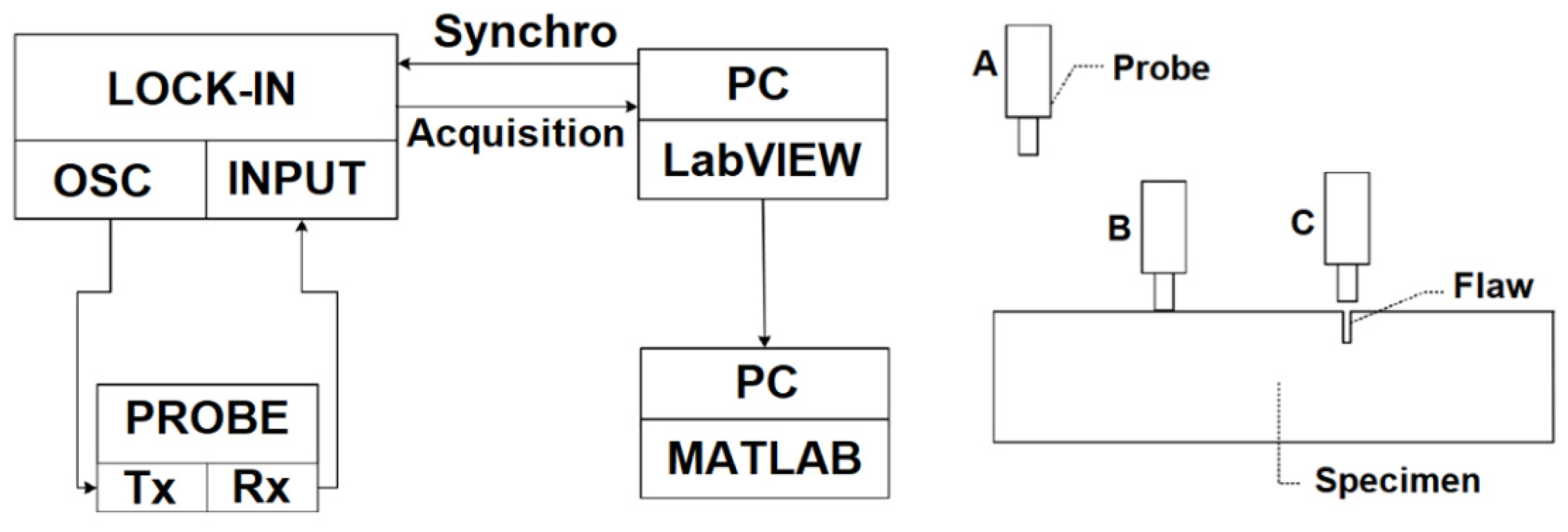
Figure 10.
Experimental results: specimen No. 1, differential voltage magnitude on frequency dependences (left) and phase dependences on differential voltage magnitude (right) for individual flaw depths, probe A.
Figure 10.
Experimental results: specimen No. 1, differential voltage magnitude on frequency dependences (left) and phase dependences on differential voltage magnitude (right) for individual flaw depths, probe A.
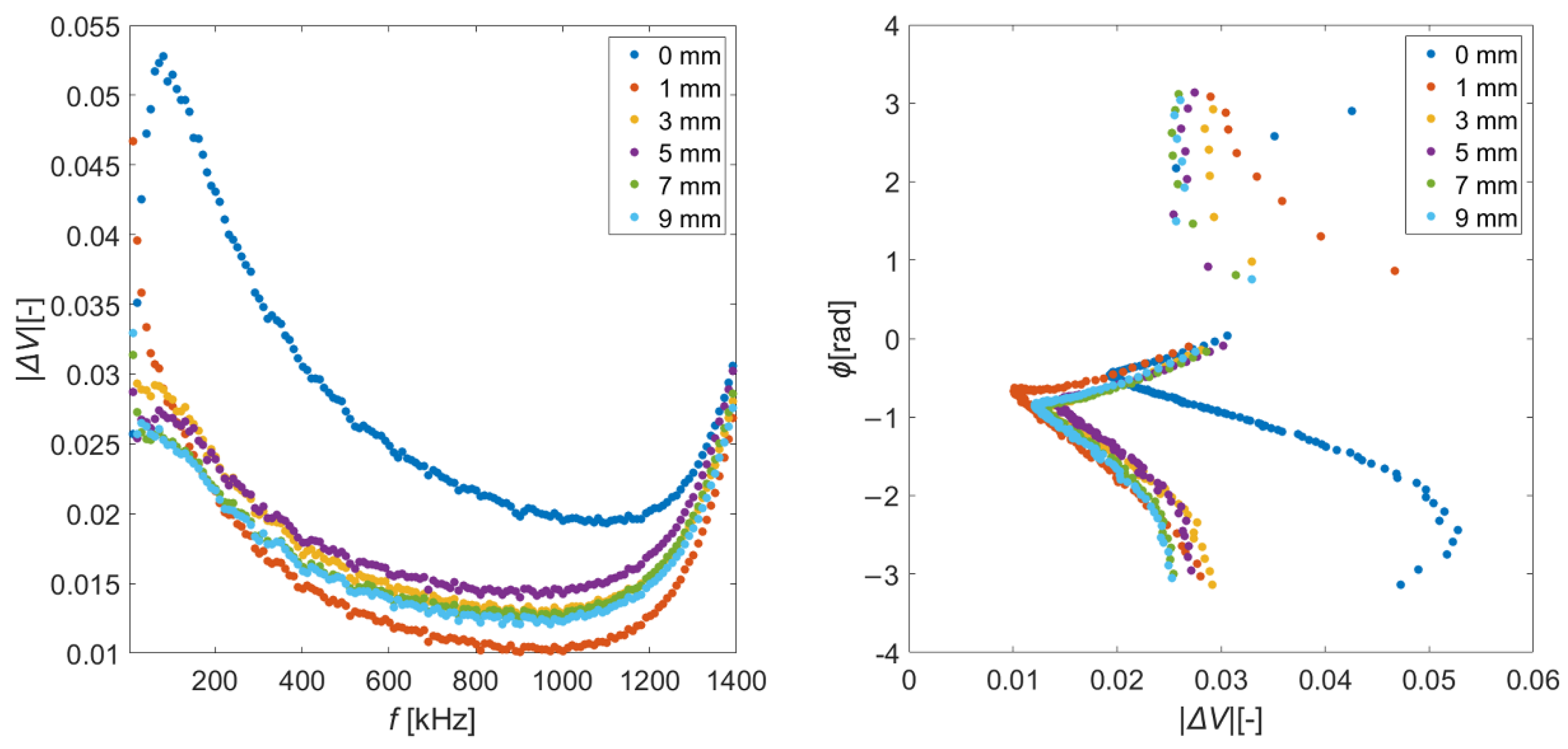
Figure 11.
Experimental results: specimen No. 1, differential voltage magnitude on frequency dependences (left) and phase dependences on differential voltage magnitude (right) for individual flaw depths, probe B.
Figure 11.
Experimental results: specimen No. 1, differential voltage magnitude on frequency dependences (left) and phase dependences on differential voltage magnitude (right) for individual flaw depths, probe B.
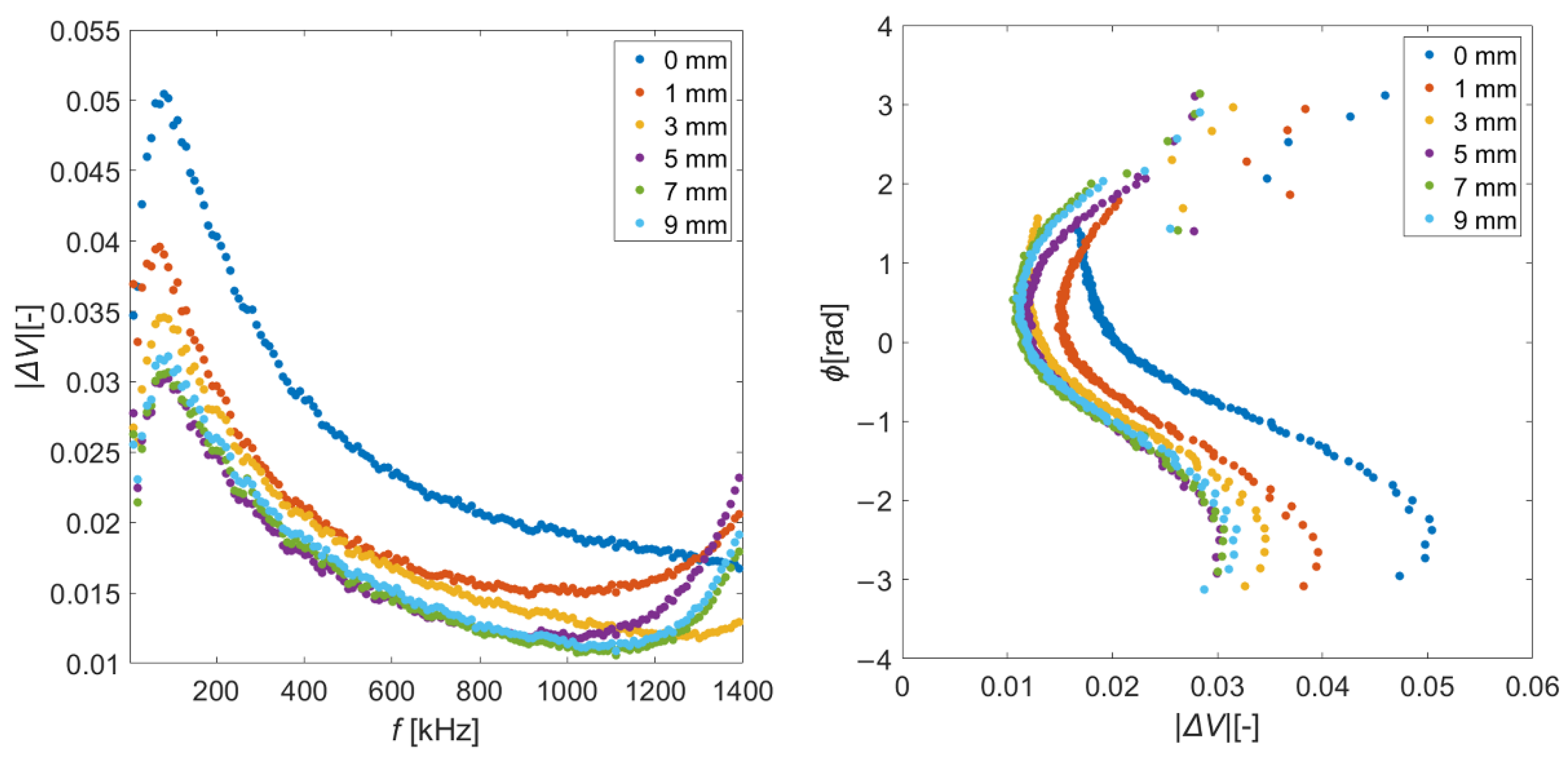
Figure 12.
Experimental results: specimen No. 1, differential voltage magnitude on frequency dependences (left) and phase dependences on differential voltage magnitude (right) for individual flaw depths, probe C.
Figure 12.
Experimental results: specimen No. 1, differential voltage magnitude on frequency dependences (left) and phase dependences on differential voltage magnitude (right) for individual flaw depths, probe C.
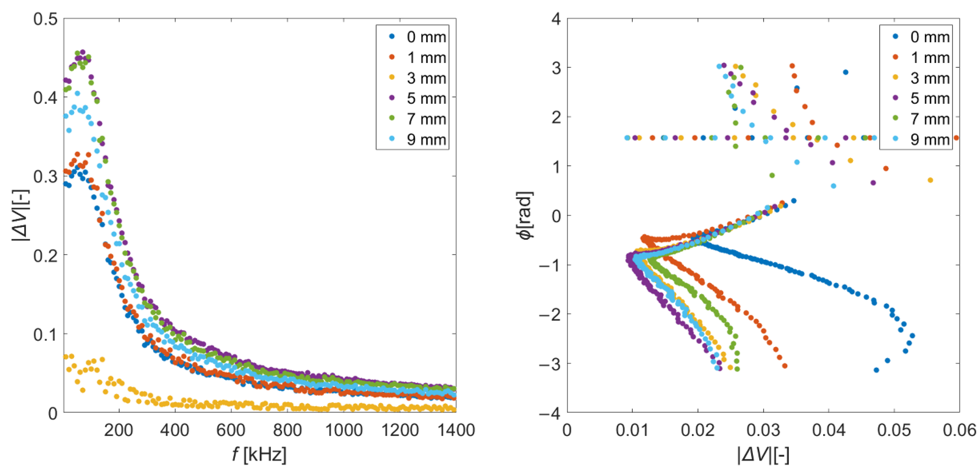
Figure 13.
Experimental results: specimen No. 2, differential voltage magnitude on frequency dependences (left) and phase dependences on differential voltage magnitude (right) for individual flaw depths, probe A.
Figure 13.
Experimental results: specimen No. 2, differential voltage magnitude on frequency dependences (left) and phase dependences on differential voltage magnitude (right) for individual flaw depths, probe A.

Figure 14.
Experimental results: specimen No. 2, differential voltage magnitude on frequency dependences (left) and phase dependences on differential voltage magnitude (right) for individual flaw depths, probe B.
Figure 14.
Experimental results: specimen No. 2, differential voltage magnitude on frequency dependences (left) and phase dependences on differential voltage magnitude (right) for individual flaw depths, probe B.

Figure 15.
Experimental results: specimen No.2, differential voltage magnitude on frequency dependences (left) and phase dependences on differential voltage magnitude (right) for individual flaw depths, probe C.
Figure 15.
Experimental results: specimen No.2, differential voltage magnitude on frequency dependences (left) and phase dependences on differential voltage magnitude (right) for individual flaw depths, probe C.
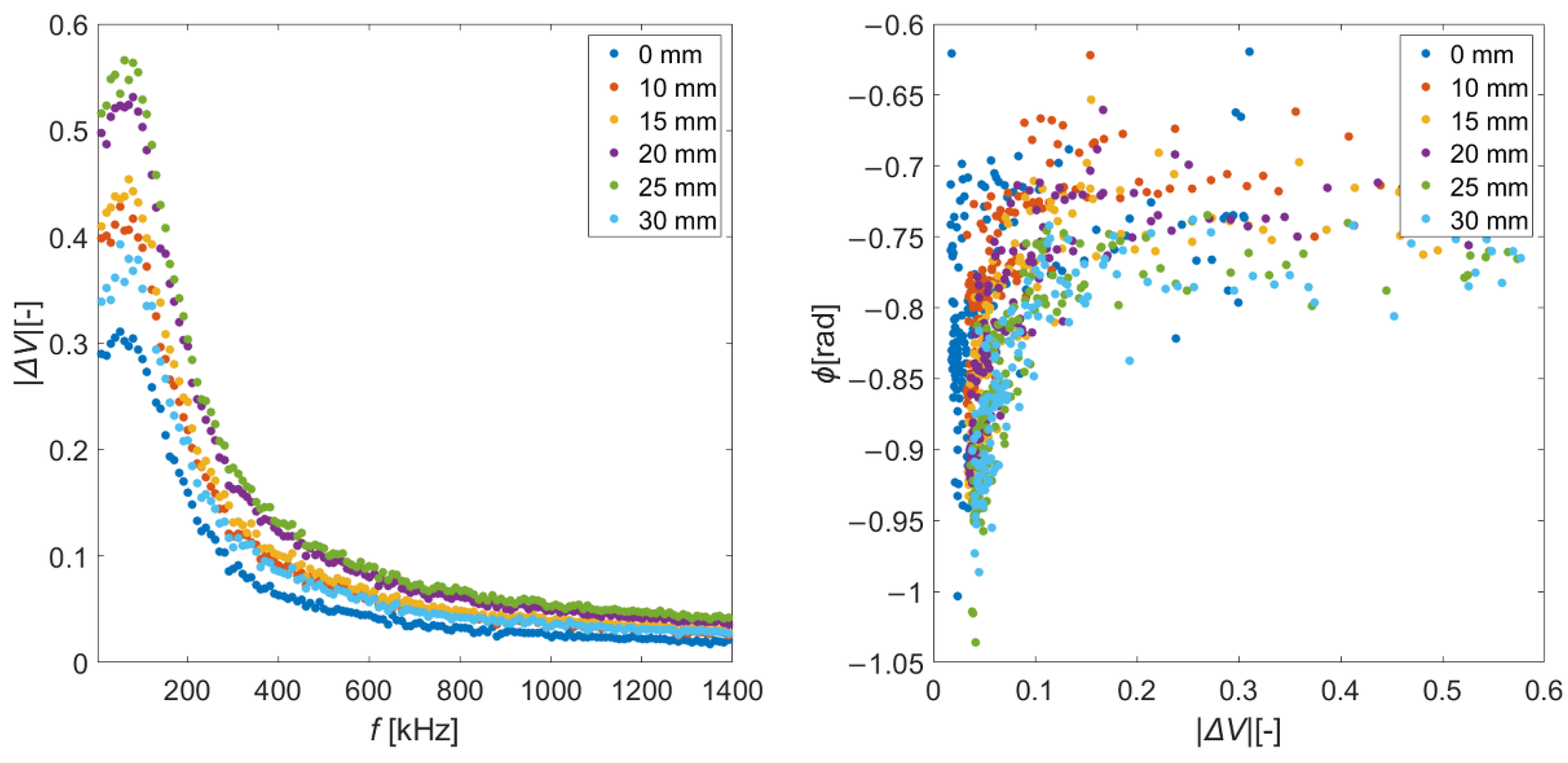
Figure 16.
Difference between simulation and experimental results for individual flaws, specimen No.1: probe A (left), probe B (middle), and probe C (right).
Figure 16.
Difference between simulation and experimental results for individual flaws, specimen No.1: probe A (left), probe B (middle), and probe C (right).
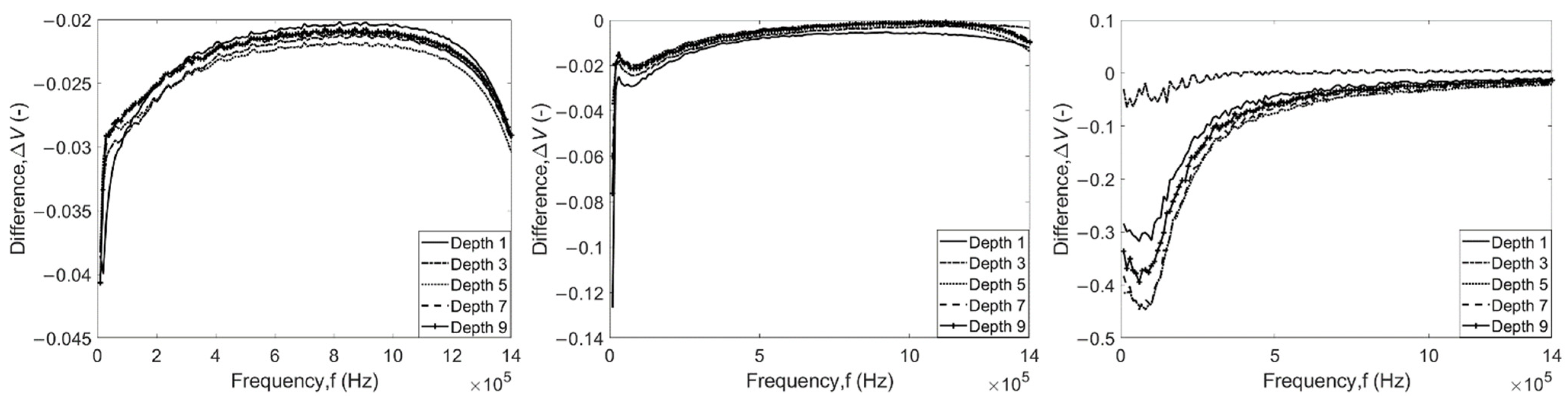
Figure 17.
Experimental results: constructed dependences, probes A, B and C; normalized current density module on defect length.
Figure 17.
Experimental results: constructed dependences, probes A, B and C; normalized current density module on defect length.
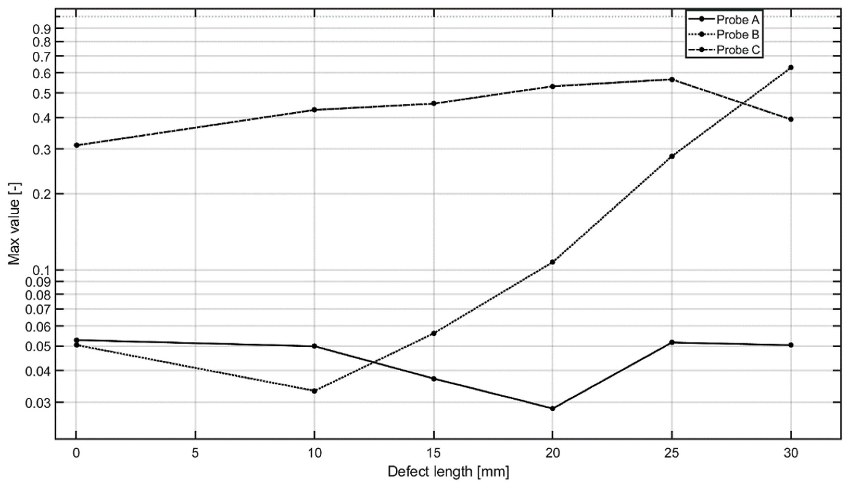
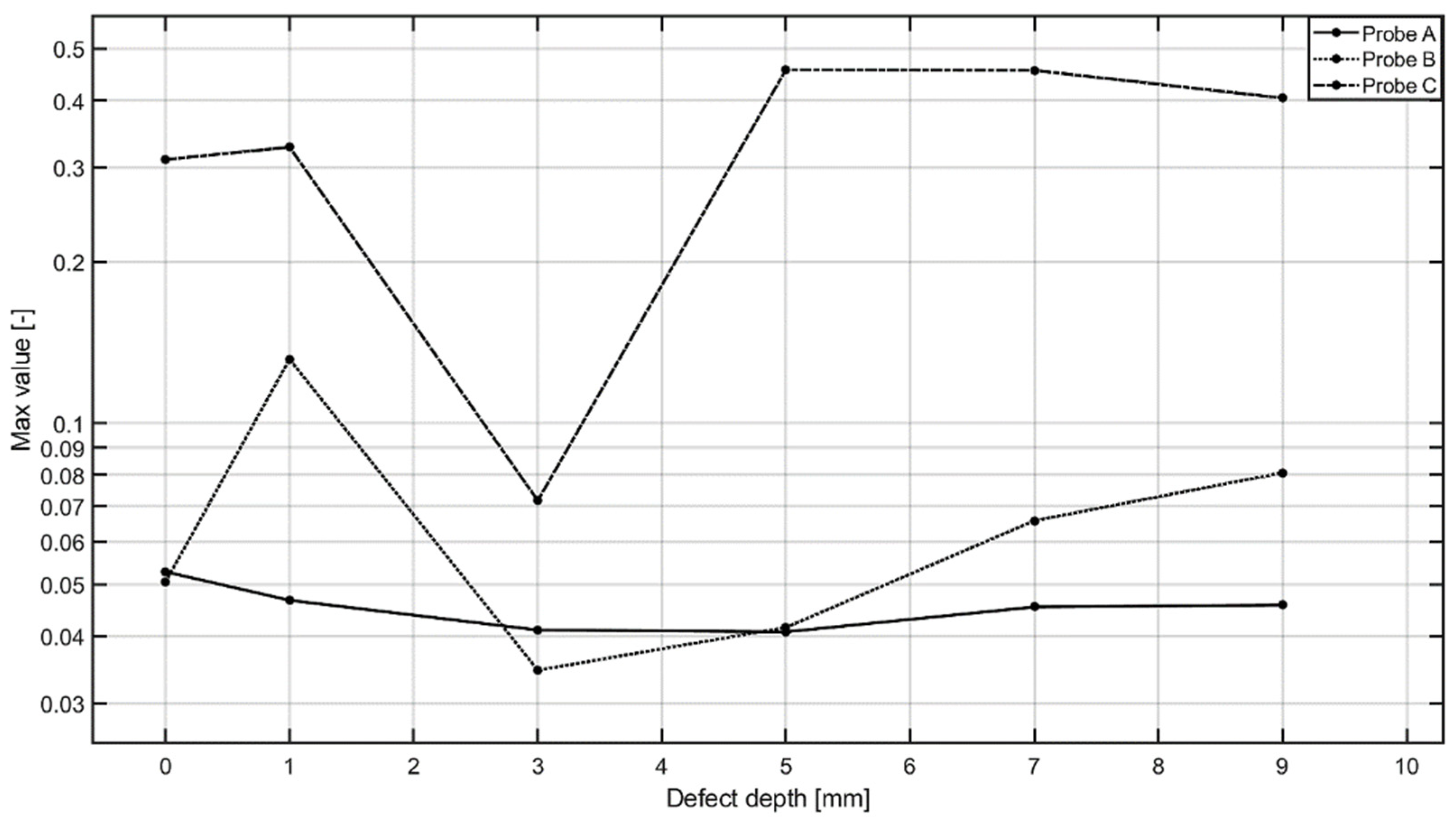
Figure 18.
Experimental results: constructed dependences, probes A, B and C; normalized current density module on defect depth.
Figure 18.
Experimental results: constructed dependences, probes A, B and C; normalized current density module on defect depth.

Table 1.
The SFECT probes simulated parameters.
| Attribute | Symbol | Value |
|---|---|---|
| Rx width | wRx | 0.7 mm |
| Rx height | hRx | 2 mm |
| Rx radius | rcoil | 1.4 mm |
| Rx number of turns | NRx | 140 |
| Tx width | wTx | 0.5 mm |
| Tx height | hTx | 2 mm |
| Tx radius | rcoil | 1.4 mm |
| Tx number of turns | NTx | 80 |
| Tx-Rx lift off | hlo | 0.8 mm |
| Core height | hc | 5.7 mm |
| Core radius | rc | 0.55 mm |
| Core relative permeability | μcore | 13,000 |
| Shielding width | wsh | 1 mm |
Table 2.
Detailed geometry of the inspected flaws presented at individual material specimens.
| Flaw No. | Specimen 1 | Specimen 2 |
|---|---|---|
| Flaw 1 | dsp1 = 1 mm | dsp2 = 5 mm |
| lsp1 = 10 mm | lsp2 = 10 mm | |
| wsp1 = 0.25 mm | wsp2 = 0.25 mm | |
| Flaw 2 | dsp1 = 3 mm | dsp2 = 5 mm |
| lsp1 = 10 mm | lsp2 = 15 mm | |
| wsp1 = 0.25 mm | wsp2 = 0.25 mm | |
| Flaw 3 | dsp1 = 5 mm | dsp2 = 5 mm |
| lsp1 = 10 mm | lsp2 = 20 mm | |
| wsp1 = 0.25 mm | wsp2 = 0.25 mm | |
| Flaw 4 | dsp1 = 7 mm | dsp2 = 5 mm |
| lsp1 = 10 mm | lsp2 = 25 mm | |
| wsp1 = 0.25 mm | wsp2 = 0.25 mm | |
| Flaw 5 | dsp1 = 9 mm | dsp2 = 5 mm |
| lsp1 = 10 mm | lsp2 = 30 mm | |
| wsp1 = 0.25 mm | wsp2 = 0.25 mm |
Table 3.
Median and standard deviation (StD) values of differences among parameters obtained by numerical and experimental means.
Table 3.
Median and standard deviation (StD) values of differences among parameters obtained by numerical and experimental means.
| Parameter | Probe A | Probe B | Probe C | |
|---|---|---|---|---|
| Depth | Median | −0.0049 | −0.0059 | −0.028 |
| StD | 0.0079 | 0.0084 | 0.1023 | |
| Length | Median | −0.0043 | −0.0067 | −0.0467 |
| StD | 0.0083 | 0.0254 | 0.1251 | |
Publisher’s Note: MDPI stays neutral with regard to jurisdictional claims in published maps and institutional affiliations. |
© 2022 by the authors. Licensee MDPI, Basel, Switzerland. This article is an open access article distributed under the terms and conditions of the Creative Commons Attribution (CC BY) license (https://creativecommons.org/licenses/by/4.0/).
Share and Cite
MDPI and ACS Style
Vaverka, F.; Smetana, M.; Gombarska, D.; Janousek, L. Diagnosis of Artificial Flaws from Eddy Current Testing Signals Based on Sweep Frequency Non-Destructive Evaluation. Appl. Sci. 2022, 12, 3732. https://doi.org/10.3390/app12083732
AMA Style
Vaverka F, Smetana M, Gombarska D, Janousek L. Diagnosis of Artificial Flaws from Eddy Current Testing Signals Based on Sweep Frequency Non-Destructive Evaluation. Applied Sciences. 2022; 12(8):3732. https://doi.org/10.3390/app12083732
Chicago/Turabian StyleVaverka, Filip, Milan Smetana, Daniela Gombarska, and Ladislav Janousek. 2022. "Diagnosis of Artificial Flaws from Eddy Current Testing Signals Based on Sweep Frequency Non-Destructive Evaluation" Applied Sciences 12, no. 8: 3732. https://doi.org/10.3390/app12083732
Note that from the first issue of 2016, this journal uses article numbers instead of page numbers. See further details here.