

Conclusive Model-Fit Current–Voltage Characteristic Curves with Kink Effects
Department of Electronic Engineering, Ming Hsin University of Science and Technology, Hsinchu 30401, Taiwan
*
Author to whom correspondence should be addressed.
Appl. Sci. 2023, 13(22), 12379; https://doi.org/10.3390/app132212379
Submission received: 30 September 2023
/
Revised: 8 November 2023
/
Accepted: 9 November 2023
/
Published: 16 November 2023
(This article belongs to the Topic Innovation of Applied System)
Abstract
:Current–voltage characteristic curves of NFinFET are presented and fitted with modified current–voltage (I-V) formulas, where the modified term in the triode region is demonstrated to be indispensable. In the as-known I-V formula, important parameters need to be determined to make both the measured data and the fitting data as close as possible. These parameters include kN (associated with the sizes of the transistor and mobility), λ (associated with early voltage), and Vth (the threshold voltage). The differences between the measured data and the fitting data vary with the applied source–drain bias, proving that the mobility of the carriers is not consistently constant. On the other hand, a modified formula, called the kink effect factor, is negatively or positively added, simulating solitary heat waves or lattice vibration, which disturb the propagation of carriers and thus influence the source–drain current (IDS). The new statistical standard deviations (δ) are then found to be effectively suppressed as the kink effect is taken into account.
1. Introduction
Transistors fabricated in the semiconductor industry successfully achieve various desired functions, including signal processing, data calculation, and decision making. All the functions are associated with memory transfer at a comparable speed. So, the size of the transistor continues to shrink, not mainly for the benefits of increasing the number of integrated circuits (IC). The speed of the ICs somehow becomes the pursued goal. Three concerns appear manifested in a sense. They are the outrageous loss of controllability, unavoidable heat, and unexpected limitations of photolithographs. The controllability, closely related to the leakage current, is due to proportional dimension shrinkage, even if some adopted prevention, including halo implant or pocket implant, is taken into account at the planar device level. In addition, the promotion of electrical performance at the same scale using the compressive or tensile stress technique is seriously considered as well. Unfortunately, channel lengths below tens of nanometers seem not to work out any more as desired, no matter what has been adopted. Instead of a planar bulk silicon substrate, there comes a 3D structural fin-like field effect transistor (FinFET) and gates all around the field effect transistor (GAAFET), which make use of a slim strip of epitaxial silicon as a body substrate wrapped by insulator-separated gate poly-silicon. The strip of channel substrate is depleted as the gate poly-silicon is applied with a bias. This bias causes the depletion region of the substrate strip to impressively and effectively block the leakage current in between the source and drain. As for the generated heat, it is basically linked to the equivalent resistors, whose resistance is actually proportional to the length of the resistor and inversely dependent on the area of the cross-section. The resistance of the decreasing dimension soars, making the increasing Ohm’s heat tremendously degrade its electrical performance and thus competitively lose leading status. Therefore, the conduction of heat dominates the whole process flow and material choice. Copper is thus preferred for its higher conductivity. The exposure of ultra-violet rays suggests diffraction immunity, which is identified as the use of a shorter wavelength, improvement in the refraction angle (refractive index, n), and subtle design and combination of masks. Traditional optics and modern optics are both utilized or designed to resolve diffraction issues.
Furthermore, the electrical performances for any transistor have to be reliable and repeatable. Models are thus proposed to address these electrical performances. They are able to fit the measured characteristic curves. All the circuit designs, including analog and digital, rely solely on the established model. Research has to be undertaken to understand the electrical data. The most commonly used formulas have been posed for over many decades, and they surely reduce the tremendous work on the design level. Therefore, current-versus-voltage characteristic curves showing the electrical performances of transistors are necessarily parameter-extracted in the model. Nevertheless, researchers are still intrigued to know if the “modified” conventional formula is applicable for fitting repeated characteristic curves [1,2,3,4,5,6,7,8,9,10,11,12,13,14]. Useful parameters are supposed to be constants in the model, even though they need interpreting. For example, mobility is a constant at a certain fixed VGS. But the mobility may be different at different VGS [15].
Moreover, one thing that causes attention is carriers traveling in crystallized silicon, which is a diamond structure. The crystal thermally vibrates at a certain temperature, causing trouble for the carriers. As the carriers speed up, they confront more obstacles. More obstacles generate more heat and more friction, which may slow down the carriers, especially in the triode region. For example, in our daily life, rain falls at an almost constant terminal speed near the ground, addressing a similar situation.
In this study, the as-measured (IDS and VDS) data are referred to the transistors fabricated using the 3D FinFET structure process. Each piece of (IDS and VDS) data corresponds to the terminal speed that determines the IDS at the applied bias, VDS. The “modified” conventional I-V characteristic curve formulas in Equation (1) with λ (the inverse of the absolute value of the early voltage, VA) are deliberately introduced in the triode region for a VDS less than (VGS-Vth), whereas Equation (2) is kept unchanged for the saturation regime. A delta deviation in Equation (3) for the whole fitting is suggested and effectively reduces the discrepancy between the fitting data and the measured data. In addition, the solution to a non-linear differential equation, called the sine-Gordon equation, is first proposed for addressing a solitary wave, which is some kind of phonon coming from quantized sounds or vibrations. The drawn curve of the function of this nonlinear solution against time is intriguing, because the curve is quite similar to the characteristic curves of MOSFET transistors or bipolar transistors. The derivative of the solution is proven to be somewhat Gaussian and is introduced to further reduce the delta deviation in the electrical characteristic curves, which is really encouraging. A transistor with a channel length L = 100 nm is first posed to demonstrate the fitting capability without or with a kink effect. For transistors with a longer channel length, such as a 180 nm long transistor, fittings without or with kink are again tried and shown to be useful even with a gate bias as high as 3 V applied. Finally, newer data at channel length L = 90 nm are then expected to repeat the same as that proposed.
2. Preparation of as Measured Data and Fitting
2.1. Preparation
The as-measured (IDS and VDS) data are obtained through the probe station on FinFET technology, which uses epitaxial silicon grown on silicon wafer and a dry-etched floated island “I” with two head ends as the source and drain and the channel in between two ends. The dry oxide of 14 angstrom film on the slim sides of the floated island “I” followed by 4000 angstrom poly-silicon as Gate makes the transistor look like a fin after polysilicon dry-etching. The measured data and self-generated data coming from the modified conventional formulas in Equations (1) and (2), as following in the next paragraph, are merged into one graph for a comparison of fitting.
2.2. Fitting IDS-VDS and IDS-VGS
For MOSFET devices, the commonly conventional formula is derived as follows by starting with JDS, the current density:
where W and D denote the channel width and channel depth after strong inversion, n means the density of the carriers, and e = 1.6 × 10⁻¹⁹ coulomb signifies the charge of the carriers. Also, neD = Q(1) = C(1)ΔV = C(1)(VGS−Vth−V) is treated as the carrier charge per unit area charging in the unit capacitance C(1), and μ (the mobility of carriers) is treated as a constant at a fixed VGS for the integration over the channel voltage from 0 V to VDS. In addition, the term, (1 + λVDS), is deliberately added in the triode region as compared to the conventional one when both the short-channel effect and charging sharing model are taken into account to address the channel length, L = Lo(1 + ΔL/Lo). The modified formulas are then proposed in Equation (1):
and
Somehow, without or with the added term, (1 + λVDS), in the triode region in Equation (1), the discontinuity may appear or disappear as the triode region goes on to the saturation region, as shown in Figure 1. The coefficients (α and β) in Equations (1) and (2) are referencing parameters for the kink effects. α (A) is mainly the maximum subtracted or added current, and β (1/V2) is from −10 to −20, depending on how wide the kink is. χ is always found to be located around χ = VGS − Vth.
2.3. The Delta Deviation
The fitting data from Equations (1) and (2) are deliberately used to fit the as-measured I-V characteristic curves. Those parameters are mainly determined predominantly according to the minimum delta (δ) in the following Equation (3):
2.4. The Kink Effect
The gate bias strongly inverses the channel layer, whose thickness is about 200 Angstroms [15,16]. The collective free carriers (electrons) travel through the channel, which is a grossly periodic diamond structure of silicon (double face-center cubic). For simplicity, the electrons are assumed to travel in one dimension from source to drain (1, 0, 0) via center to center or corner to corner. Even if those carriers are collective, the interactions among them are thought to be weak enough to be ignored, such that each of them is treated as individual without losing generality. The variation in the potential energy of an electron is realized as sinusoid due to the periodic diamond structure. A free electron is also supposed to surpass the attraction force from the field of the periodic ion cores. Therefore, instead of V = Vo [1 − cos(2πx/lo)], with lo as a periodic referencing length, the potential energy density is deliberately written as V(ϕe) = (a/b)[1 − cos(bϕe)], where V(ϕe) is non-negative. Actually, ϕe inside the argument is nothing new, e.g., the differential equation of the azimuth angle of a pendulum swinging back and forth. An electron moves from a constant potential (ground/source) to the next constant potential (VDS/drain), where a collective IDS is measured and marked. As the VDS is increased, the corresponding collective IDS is measured and recorded again until the current becomes saturated when the applied VDS is high enough. The whole characteristics are then constructed, just like a series of (VDS and IDS) pictures, which are applicable for digital usages, amplifiers, and mixers, etc. Wherever an electron is located in the channel, the electric field varies not only because of different locations, but also because of different VDS. This may be the reason why a nonlinear equation is considered. The carriers and electrons are fermions, but there is no loss of generality to treat the electron wave function as , where obeys Fermi–Dirac statistics. The non-linear differential equation, addressing a moving electron scalar field, , in the strongly inversed layer, refers to the Lagrangian as follows:
which is named as the sine-Gordon equation [18]. The moving electrons accelerated by the electrical field confront phonons with a group velocity c of thousands of meters per second in the lattice [18]. These electrons quickly reach the speeds that are sometimes higher than and sometimes lower than the so-called terminal speed. The space–time variables are adjusted with respect to the referencing frame as follows:
Equation (4) thus reduces to the following form, with b as a dimensional adjusting parameter:
The non-linear solution of Equation (5) is expressed as:
If the nonlinear solution y = arctan[exp(t/2)] versus t looks like IDS − VDS characteristic curves of transistors, such as MOSFET or Bipolar Junction Transistor (BJT), the slopes of the curves result in speed variations in the carriers that would cause heat dissipation problems, because the slope maximum is equivalent to the speed maximum that causes extra heat. Referring to the IDS derivative to the VDS with the VGS fixed, the slope means the speed variations in carriers, which may cause a heat dissipation issue and thus a corresponding mini-scale impact on adjusting the speeds of the carriers microscopically. The peak of the derivatives is always at the center, meaning that the maximum changing pace leaves heat radiation, called Bremsstrahlung radiation, or braking radiation. Some other similar examples like synchrotron radiation may happen. These radiations causing the corresponding current corrections are intrinsically proportional to the slope (the peak, which is proven to be Gaussian-like).
3. Application
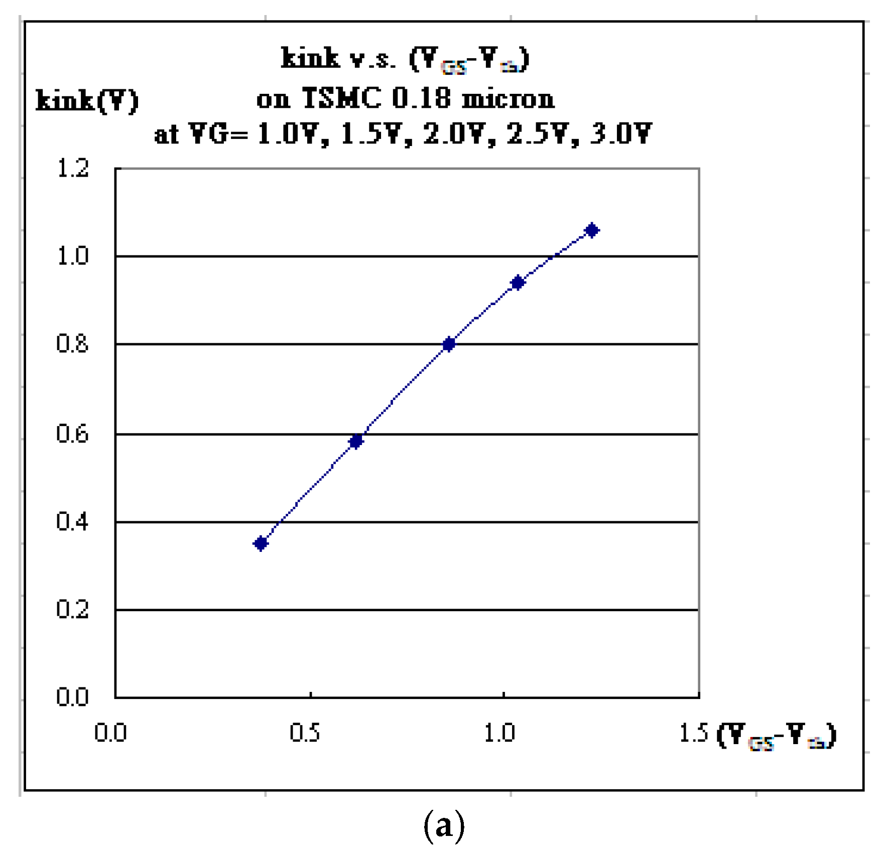
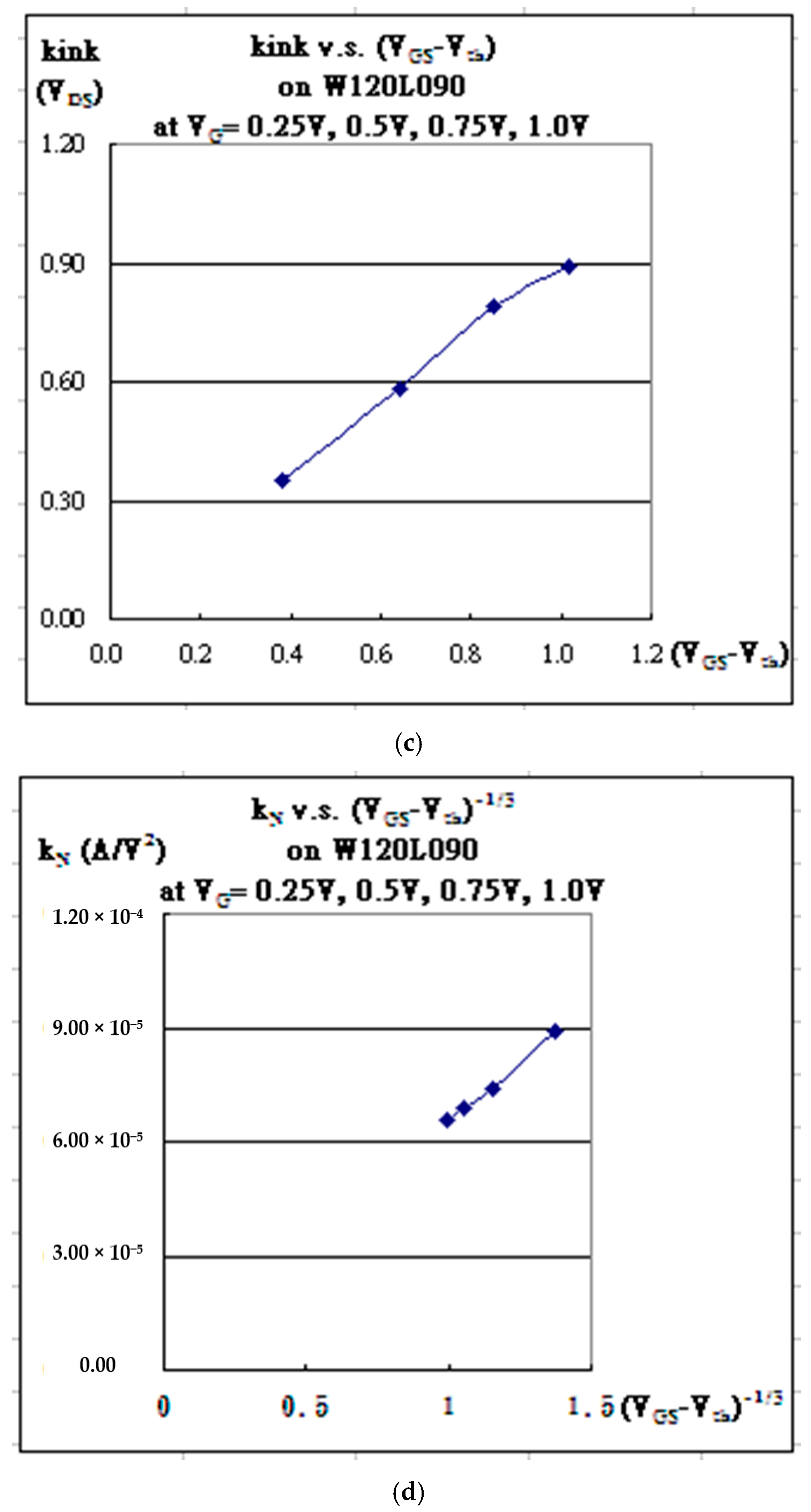
The minimum delta (δ) in Equation (3) can be used to determine the chosen parameters without considering kink effects, which are listed in Table 1 [8]. In the table, the minimum delta at different gate biases requires different kn, lambda (λ), and threshold voltages. For one thing, the slope of lambda addressing the leakage current dominates a rough minimum delta. As referred to Figure 4a, the fitting is not as good. The differences between the fitting current and the measured current at various VDS’s are demonstrated in Figure 4b, where the peaks at different VGS are located at different VDS, named “kinks” in Table 1. Surprisingly, the strong correlation gives a straight line passing the origin as the kink is plotted against (VGS − Vth), as shown in Figure 5a. That is to say, the kink is always proportional to (VGS − Vth). In addition, kN containing mobility, μ, is proportional to (VGS − Vth)−1/3, as shown in Figure 5b [15].
With taking kink effects into account, as shown in Figure 5, the deviation (delta) can be suppressed as low as 10−7, and the fitting is improved a lot in Figure 5c,d. When turning off kink effects, as shown in Figure 5a,b, the fitting curves are always lifted up at VDS ~ (VGS − Vth) as compared to the as-measured data. To take care of the issue in which fitting curves are commonly lower than as-measured currents, the kink effects are thus considered. The solitary waves can be in thermal form, or maybe in phonons. The electron might be deflected because of collisions with phonons, and those collisions may cause the degradation of electrical performances. The item is thus introduced and subtracted, which is proportional to the exponential with the Gaussian form, as seen in Equations (1) and (2). In Figure 5c,d, the fitting is really encouraging. The enlarged figure in Figure 5d does enhance the fitting.
4. Discussions
The as-measured data redrawn as characteristic curves can be fitted with the ones based on the modified conventional current–voltage formula. Even though it is quite engineering, such a fitting may be quite easy to be undertaken. The parameters are easily determined if the parameters are not required to keep the same. Instead, the trends or scales of some specific parameters always give some information [16,17]. Moreover, the kink effects really exist, as referred to Figure 4a,b, for the 0.18-micron process, where the determined parameters for characteristic curves are listed in Table 1, as well as Figure 6a,b for the 0.09-micron process, where the determined parameters for characteristic curves are listed in Table 2. A kink effect model will efficiently help to work out the fitting, e.g., the sets, (Figure 4a,b, Figure 5c,d, Figure 6a,b and Figure 7a,b), where the minimum delta (δ) is highly reduced, as expected.
By comparing the FinFET 0.09-micron process with the TSMC 0.18-micron process, both share the same characteristics: one is for where the kinks are located and the other is for the electrical-field-associated mobility. As demonstrated in Figure 5a,c, kinks, χ’s, are almost located at VDS, which is linearly dependent on (VGS − Vth), meaning that there exists a strong correlation between the kink and the connection at the end of the triode region. Also, Figure 5b,d show that kN tends to be proportional to (VGS − Vth)−1/3 and that the mobility (μ) of the carriers is then understood to be due to delaying effects at the interface of the strongly inversed layer with the oxide, as shown in Equation (8): [15]
As for α and β in Equations (1) and (2), the maximum discrepancy between the fitting current and the measured current always helps to identify α, while the width of the kinks at a certain VGS determines what β value is more adequate. Both parameters are intriguing to explore profoundly in the near future [19].
Nevertheless, a model might be useful, especially for circuit design, including digital and analog circuits. A useful generated model provides well-fitted curves and matches the measured characteristic curves as possible as expected. In this study, some parameters are used to fit the characteristic curves, which, instead of using many equivalent circuits to complete the fitting, is thought to be more practical and feasible. Once the process technique is mature and all the transistors repeat from wafer to wafer, there will be stable manufacturing that supports the model establishment [20].
5. Conclusions
The as-measured current–voltage characteristic curves are fitted with three main parameters, (kN, Vth, and λ). In this study, the cited kinks are supposed to be associated heat or phonons, and the eliminations of those kinks make the fitting more advisable. Of course, identifying α, β, and χ in Equations (1) and (2) may be according to the preliminary fitting results. Furthermore, the abstracted kN is associated with the mobility, which is dependent on the applied gate biases. Wishfully, in the near future, the Vth and λ may help to provide extra information after fitting as well. This fitting algorithm may be a feasible way of helping to profoundly understand transistors.
Author Contributions
Conceptualization, H.-C.Y. and S.-C.C.; methodology, H.-C.Y. and S.-C.C.; software, H.-C.Y. and S.-C.C.; validation, H.-C.Y. and S.-C.C.; formal analysis, H.-C.Y. and S.-C.C.; investigation, H.-C.Y. and S.-C.C.; resources, H.-C.Y. and S.-C.C.; data duration, H.-C.Y. and S.-C.C. All authors have read and agreed to the published version of the manuscript.
Funding
This research received no external funding.
Institutional Review Board Statement
Not available.
Informed Consent Statement
Not available.
Data Availability Statement
The data presented in this study are available on request from the corresponding author. The data are not publicly available due to privately continuing working on a final algorithm.
Conflicts of Interest
The authors declare no conflict of interest.
References
- Diab, A.; Torres Sevilla, G.-A.; Christoloveanu, S.; Hussain, M.-M. Room to high temperature measurements of flexible SOI FinFETs with sub-20-nm fins. IEEE Trans. Electron. Devices 2014, 61, 3978. [Google Scholar] [CrossRef]
- Wang, F.; Xie, Y.; Bernstein, K.; Luo, Y. Dependability analysis of nano-scale FinFET circuits. In Proceedings of the IEEE Computer Society Annual Symposium on Emerging VLSI Technologies and Architectures (ISVLSI’06), Karlsruhe, Germany, 2–3 March 2006; p. 6. [Google Scholar]
- Huang, X.; Lee, W.-C.; Kuo, C.; Hisamoto, D.; Chang, L.; Kedzierski, J.; Anderson, E.; Takeuchi, H.; Choi, Y.-K.; Asano, K.; et al. Sub-50 nm P-channel FinFET. IEEE Trans. Electron. Devices 2001, 48, 880. [Google Scholar] [CrossRef]
- Rudenko, T.; Kilchytska, V.; Arshad, M.K.M.; Raskin, J.-P.; Nazarov, A.; Flandre, D. On the MOSFET Threshold Voltage Extraction by Transconductance and Transconductance-to-Current Ratio Change Methods: Part II-Effect of Drain Voltage. IEEE Trans. Electron. Devices 2011, 58, 4180–4188. [Google Scholar] [CrossRef]
- Takahashi, T.; Beppu, N.; Chen, K.; Oda, S.; Uchida, K. Self-heating effects and analog performance optimization of Fin-type field-effect transistors. Jpn. J. Appl. Phys. 2013, 52, 04CC03. [Google Scholar] [CrossRef]
- Saitoh, M.; Yasutake, N.; Nakabayashi, Y.; Uchida, K.; Numata, T. Understanding of strain effects on high-field carrier velocity in (100) and (110) CMOSFETs under quasi-ballistic transport. In Proceedings of the 2009 IEEE International Electron Devices Meeting (IEDM), Baltimore, MD, USA, 7–9 December 2009; pp. 1–4. [Google Scholar]
- Chen, C.W.; Wang, S.J.; Hsieh, W.C.; Chen, J.M.; Jong, T.; Lan, W.H.; Wang, M.C. Q-factor Performance of 28 nm-node High-k Gate Dielectric under DPN Treatment at Different Annealing Temperatures. Electronics 2020, 9, 2086. [Google Scholar] [CrossRef]
- Lu, P.; Yang, C.; Li, Y.; Li, B.; Han, Z. Three-Dimensional TID Hardening Design for 14 nm Node SOI FinFETs. Eng 2021, 2, 620–631. [Google Scholar] [CrossRef]
- Song, Y.S.; Tayal, S.; Rahi, S.B.; Kim, J.H.; Upadhyay, A.K.; Park, B.-G. Thermal-Aware IC Chip Design by Combining High Thermal Conductivity Materials and GAA MOSFET. In Proceedings of the 2022 5th International Conference on Circuits, Systems and Simulation (ICCSS), Nanjing, China, 13–15 May 2022; pp. 135–140. [Google Scholar]
- Crupi, G.; Schreurs, D.M.M.-P.; Caddemi, A.; Angelov, I.; Homayouni, M.; Raffo, A.; Vannini, G.; Parvais, B. Purely analytical extraction of an improved nonlinear FinFET model including non-quasi-static effects. Microelectron. Eng. 2009, 86, 2283–2289. [Google Scholar] [CrossRef]
- Li, Y.; Zhao, F.; Cheng, X.; Liu, H.; Zan, Y.; Li, J.; Zhang, Q.; Wu, Z.; Luo, J.; Wang, W. Four-Period Vertically Stacked SiGe/Si Channel FinFET Fabrication and Its Electrical Characteristics. Nanomaterials 2021, 11, 1689. [Google Scholar] [CrossRef] [PubMed]
- Zhao, E.; Zhang, J.; Salman, A.; Subba, N.; Chan, J.; Marathe, A.; Beebe, S.; Taylor, K. Reliability challenges of high performance PD SOI CMOS with ultra-thin gate dielectrics. Solid State Electron. 2004, 48, 1703–1708. [Google Scholar] [CrossRef]
- Zhao, Z.Q.; Li, Y.; Zan, Y.; Li, Y.L.; Li, J.J.; Cheng, X.H.; Wang, G.L.; Liu, H.Y.; Wang, H.X.; Zhang, Q.Z.; et al. Fabrication technique of the Si0.5Ge0.5 Fin for the high mobility channel FinFET device. Semicond. Sci. Technol. 2020, 35, 045015. [Google Scholar] [CrossRef]
- Lee, J.; Park, T.; Ahn, H.; Kwak, J.; Moon, T.; Shin, C. Prediction Model for Random Variation in FinFET Induced by Line-Edge-Roughness (LER). Electronics 2021, 10, 455. [Google Scholar] [CrossRef]
- Van Zeghbroeck, B. Priciples of Semiconductor Devices, Chapter 7.6 Advanced MOSFET Issues. Available online: http://ece-www.colorado.edu/~bart/book/book/title.htm (accessed on 30 September 2023).
- Yang, H.-C.; Chi, S.-C. Process Corresponding Implications Associated with a Conclusive Model-Fit Current-Voltage Characteristic Curves. Appl. Sci. 2022, 12, 462. [Google Scholar] [CrossRef]
- Yang, H.-C.; Chi, S.-C.; Liao, W.S. Comparison of Fitting Current–Voltage Characteristics Curves of FinFET Transistors with Various Fixed Parameter. Appl. Sci. 2022, 12, 10519. [Google Scholar] [CrossRef]
- Lewis, H. Ryder, Quantum Field Theory, Chapter 10.1 The Sine-Gordon Kink; Press Syndicate of the University of Cambridge: Cambridge, UK, 1985; p. 402. ISBN 0-521-23764-5. [Google Scholar]
- Lacroix, D.; Traore, I.; Fumwron, S.; Jeandel, G. Phonon transport in silicon, influence of the dispersion properties choice on the description of the anharmonics resistive mechanisms. Eur. Phys. J. B 2009, 67, 15–25. [Google Scholar] [CrossRef]
- Kang, S.-M.; Leblebici, Y. CMOS Digital Integrated Circuits: Analysis and Design, Chapter 4 Modeling of MOS Transistors Using SPICE; McGRAW-Hill: New York, NY, USA, 1996; p. 111. ISBN 0-07-114423-4. [Google Scholar]
Figure 1.
IDS-VDS characteristic curves of FinFET transistor (fin width = 120 nm and channel length = 90 nm) and the corresponding fitting (a) without the term, (1 + λVDS), in the triode region in Equation (1) and (b) with the term, (1 + λVDS), in the triode region in Equation (1).
Figure 1.
IDS-VDS characteristic curves of FinFET transistor (fin width = 120 nm and channel length = 90 nm) and the corresponding fitting (a) without the term, (1 + λVDS), in the triode region in Equation (1) and (b) with the term, (1 + λVDS), in the triode region in Equation (1).

Figure 2.
(a) IDS-VDS characteristic curves and the corresponding fitting with minimum delta (δ) skill in the following Equation (3) (b) Nonlinear solution y = arctan[exp(t/2)] versus t looks like IDS-VDS characteristic curves with slope variations that cause heat dissipation problems because the slope maximum is equivalent to the speed maximum variation (acceleration) that causes extra heat. Bremsstralung radiation or braking radiation is then taken into account.

Figure 3.
(a) The subtraction values of IDS-VDS characteristic curves and the corresponding fitting without eliminating the Gaussian term into account. (b) with eliminating the Gaussian term into account. (c) The final corresponding fitting in Figure 3b.
Figure 3.
(a) The subtraction values of IDS-VDS characteristic curves and the corresponding fitting without eliminating the Gaussian term into account. (b) with eliminating the Gaussian term into account. (c) The final corresponding fitting in Figure 3b.


Figure 4.
Shows the 0.18 micron process (a) IDS-VDS characteristic curves and the corresponding fitting without taking kink effect factor into account. (b) The differences between the fitting current and the measured current at various VDS’s are demonstrated.
Figure 4.
Shows the 0.18 micron process (a) IDS-VDS characteristic curves and the corresponding fitting without taking kink effect factor into account. (b) The differences between the fitting current and the measured current at various VDS’s are demonstrated.

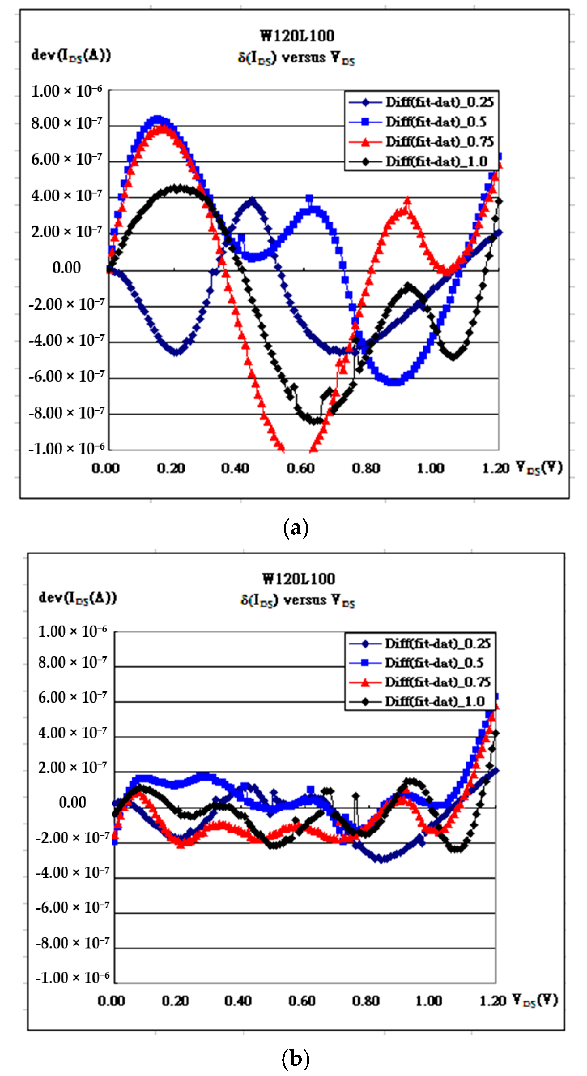
Figure 5.
TSMC 0.18 micron process (a) the strong correlation gives a straight line passing the origin as the kink is plotted against (VGS − Vth) (b) kN containing mobility, μ, is inversely proportional to (VGS − Vth)−1/3. (c) IDS − VDS characteristic curves and the corresponding fitting closely appear through elimination on kinks. (d) The differences between the fitting current and the measured current at various VDS’s are demonstrated through elimination on kinks.


Figure 6.
FinFET 0.090 micron process (a) IDS-VDS characteristic curves and the corresponding fitting without taking kink-effect factor into account. (b) The differences between the fitting current and the measured current at various VDS’s are demonstrated. Standard deviations: δ0.25 = 2.28 × 10⁻⁷, δ0.5 = 2.11 × 10⁻⁷, δ0.75 = 2.32 × 10⁻⁷, δ1.0 = 2.27 × 10⁻⁷.

Figure 7.
Shows 0.090 micron process (a) IDS − VDS characteristic curves and the corresponding fitting through elimination on kink. (b) The differences between the fitting current and the measured current at various VDS’s are demonstrated through elimination on kink. Standard deviations: δ0.25 = 5.28 × 10⁻⁸, δ0.5 = 9.78 × 10⁻⁸, δ0.75 = 6.06 × 10⁻⁸, δ1.0 = 5.88 × 10⁻⁸ (c) the strong correlation gives a straight line passing the origin as the kink is plotted against (VGS − Vth) (d) kN containing mobility, μ, is inversely proportional to (VGS − Vth)−1/3. on kinks.


Table 1.
Transistors using 0.18 micron process technology with where kink is located.
| Gate Bias (V) | kN (A/V2) | Vth_fit (V) | λ (1/V) | Kink (V) |
|---|---|---|---|---|
| VGS = 1.00 V | 0.2 | 0.625 | 0.134 | 0.35 |
| VGS = 1.50 V | 0.176 | 0.880 | 0.084 | 0.58 |
| VGS = 2.00 V | 0.156 | 1.14 | 0.048 | 0.80 |
| VGS = 2.50 V | 0.143 | 1.46 | 0.05 | 0.94 |
| VGS = 3.00 V | 0.128 | 1.78 | 0.05 | 1.06 |
Table 2.
Transistors using 0.09 micron process technology with where kink is located.
| Gate Bias (V) | kN (A/V2) | Vth_fit (V) | λ (1/V) | Kink (V) |
|---|---|---|---|---|
| VG = 0.25 V | 8.90 × 10⁻⁵ | −0.132 | 0.138 | 0.35 |
| VG = 0.50 V | 7.40 × 10⁻⁵ | −0.140 | 0.120 | 0.58 |
| VG = 0.75 V | 6.88 × 10⁻⁵ | −0.100 | 0.110 | 0.79 |
| VG = 1.00 V | 6.60 × 10⁻⁵ | −0.020 | 0.106 | 0.89 |
Disclaimer/Publisher’s Note: The statements, opinions and data contained in all publications are solely those of the individual author(s) and contributor(s) and not of MDPI and/or the editor(s). MDPI and/or the editor(s) disclaim responsibility for any injury to people or property resulting from any ideas, methods, instructions or products referred to in the content. |
© 2023 by the authors. Licensee MDPI, Basel, Switzerland. This article is an open access article distributed under the terms and conditions of the Creative Commons Attribution (CC BY) license (https://creativecommons.org/licenses/by/4.0/).
Share and Cite
MDPI and ACS Style
Yang, H.-C.; Chi, S.-C. Conclusive Model-Fit Current–Voltage Characteristic Curves with Kink Effects. Appl. Sci. 2023, 13, 12379. https://doi.org/10.3390/app132212379
AMA Style
Yang H-C, Chi S-C. Conclusive Model-Fit Current–Voltage Characteristic Curves with Kink Effects. Applied Sciences. 2023; 13(22):12379. https://doi.org/10.3390/app132212379
Chicago/Turabian StyleYang, Hsin-Chia, and Sung-Ching Chi. 2023. "Conclusive Model-Fit Current–Voltage Characteristic Curves with Kink Effects" Applied Sciences 13, no. 22: 12379. https://doi.org/10.3390/app132212379
Note that from the first issue of 2016, this journal uses article numbers instead of page numbers. See further details here.