
Design and Implementation of an IPT Charger with Minimum Number of Elements for Battery Charging Applications

1
College of Intelligent Manufacturing, Hunan University of Science and Engineering, Yongzhou 425199, China
2
College of Electronic and Electrical Engineering, Henan Normal University, Xinxiang 453007, China
*
Author to whom correspondence should be addressed.
Appl. Sci. 2023, 13(6), 3580; https://doi.org/10.3390/app13063580
Submission received: 31 December 2022
/
Revised: 1 March 2023
/
Accepted: 9 March 2023
/
Published: 10 March 2023
(This article belongs to the Special Issue Advanced Electromagnetic Energy Conversion and Wireless Power Transfer Technologies)
Abstract
:Inductive power transfer (IPT) systems have been extensively studied and incorporated into various industrial applications. An IPT system with the capability to provide constant current output (CCO) and constant voltage output (CVO) is necessary to ensure optimal battery performance. However, the resistance of the battery will continue to increase during the charging process, making it difficult for the system to realize load-independent CCO and CVO with zero phase angle (ZPA) operation. Therefore, this paper proposes an LC/S compensated IPT system, which can provide CCO and CVO at fixed frequencies. ZPA operation can be maintained in both CC and CV modes for low reactive power loss. Moreover, the total number of compensation elements of the system is minimized, with only one compensation capacitor on the receiving side, which ensures not only the low cost of the system but also a compact receiver. Finally, the correctness and feasibility of the proposed system are verified with simulations and experiments.
1. Introduction
Since traditional wired power supply methods limit the flexibility of electrical equipment and have potential safety hazards, inductive power transfer (IPT) is proposed to provide flexible and reliable power transmission. Inductive power transfer is a technology using electromagnetic fields or electromagnetic waves to transmit electrical energy contactlessly. Due to the inherent advantages of IPT, it has significant research value and broad application prospects. At present, IPT has been applied in various industrial applications, such as portable electronic devices [1,2], light-emitting diode (LED) lighting applications [3,4], biomedical implants [5,6], electric vehicles [7,8], unmanned aerial vehicles [9,10], underwater applications [11], etc.
Lithium-ion batteries are widely used as energy storage devices due to their safety, good high-temperature performance, extended service life, and high energy density [12]. It is well known that the load of the battery continues to increase during battery charging. To ensure battery performance and prolong battery life, an IPT system with stable constant current output (CCO) and constant voltage output (CVO) should be designed according to the battery charging law. Figure 1 shows a typical battery charging curve. Generally, the battery is first charged in CC mode. As the battery load continues to increase, the battery charging voltage increases. Once the charging voltage reaches a preset value, the system switches to CV mode. The charging current of the battery then gradually decreases until charging is completed.
In recent years, scholars have made many innovative attempts to design an IPT system with CCO and CVO functions. In general, IPT systems have four basic topologies, namely, series-series (SS), series-parallel (SP), parallel-series (PS), and parallel-parallel (PP) [13]. It has been proven that under specific parameters, SS and PS can provide load-independent CCO characteristics, while SP and PP can provide load-independent CVO characteristics [14,15]. To realize reliable CCO and CVO functions, in [13], the aforementioned four basic topologies are combined, and hybrid topologies combining SS and PS, and SP and PP, respectively, are proposed. In addition, refs. [16,17,18,19] all achieved CCO and CVO characteristics with ZPA operation by designing different hybrid topologies. However, the proposed structures in [13,16,17,18,19] must introduce additional AC switches and compensation elements, which increases the cost and size of the systems. Therefore, the hybrid topology switching method is not the optimal solution for achieving CCO and CVO characteristics. In view of this, the authors in [20] proposed a method to achieve CCO and CVO characteristics by changing the operating frequency. Although complex topology switching is not required, SS topology can only achieve purely resistive input impedance in CC mode. In CV mode, ZPA operation cannot be satisfied, which will inevitably lead to massive power loss. In [21], the authors proposed an S/S/P topology that can provide CCO and CVO characteristics at two frequencies. Unfortunately, the volume, weight, and cost of the receiver are increased due to a bulky filter inductor behind the rectifier in this system. In [22], Vu et al. deduced and verified that a dual LCC topology could realize CCO and CVO characteristics at two frequency points. However, due to the large number of compensation components derived from this topology, this solution suffers from the same structural drawbacks as [21]. In [23], the authors presented a new three-coil parameter design approach to achieve CCO and CVO by modifying the frequency. In addition, Tran et al. [24] comprehensively analyzed a four-coil IPT system and realized CCO and CVO functions at two distinct frequency points. However, the three-coil IPT system in [23] and the four-coil IPT system in [24] both have a rigorous mutual inductance relationship, which increases the design difficulty and instability of the system. Given this, this article proposes an LC/S compensated IPT system that can realize stable CCO and CVO characteristics under two fixed ZPA operating frequencies through reasonable parameter design. Notably, the total number of compensation elements of the system is minimized, with only one compensation capacitor on the receiving side, which ensures not only the low cost of the system, but also a compact receiver. The CLC/N compensated IPT system proposed in [25] has no compensation components on the receiving side, which further optimizes the receiving side of the system from the perspective of compactness. However, the research in [25] achieved only CCO characteristics with ZPA operation through reasonable parameter design. Therefore, the research in [25] is only suitable for CC charging applications, such as LED driving. It is worth noting that the LC/S compensated IPT system proposed in this paper is suitable for charging with fixed coupling or low fluctuation, which is the same as the hybrid topologies of [16,17,18,19] and the dual-frequency topologies of [20,21,22,23,24].
Section 2 of this article describes a basic analysis of the proposed LC/S compensated IPT system. This section provides an overall analysis of the circuit topology and the principles for realizing CCO/CVO characteristics and ZPA operation. In Section 3, the system parameter tuning scheme is given. Firstly, a simulation analysis of the loosely coupled transformer (LCT) is carried out using the electromagnetic simulation software Maxwell. Then, the design steps of the system parameters are given. Next, an equivalent model is established in MATLAB to conduct preliminary verification of the proposed IPT system. Section 4 describes the design of the system switching strategy. Section 5 describes experiments for verifying the above theoretical analysis, and the advantages of the LC/S compensated IPT system proposed in this paper are summarized. Finally, Section 6 concludes the article.
2. Circuit Model and Theoretical Analysis
2.1. Circuit Model
Figure 2 shows the circuit structure diagram of the proposed LC/S compensated IPT system. Lp and Ls represent the self-inductance of the transmitting and receiving coils, and L1 is the compensation inductance. R1, Rp, and Rs represent the parasitic resistance of the compensation inductance and coils. Since the values of R1, Rp, and Rs are very small, they can be ignored in the analysis in the interest of simplification. M represents the mutual inductance between the transmitting and receiving coils. The transmitting side of the system includes a constant DC power supply Ud, a high-frequency inverter (HFI) consisting of four MOSFETs (Q1–Q4), a series compensation inductor L1, a parallel compensation capacitor C1, and a transmission coil Lp; the receiving side includes a receiving coil Ls, a series compensation capacitor C2, and a rectifier connected in parallel with a filter capacitor CF. The full-bridge rectifier provides DC power for the battery load RL. Figure 3 shows a simplified circuit diagram of the topology, in which the square wave voltage Uin driven by the HFI and the value of the equivalent load Rac can be expressed as:
![Applsci 13 03580 g002]()
![Applsci 13 03580 g003]()
Figure 2.
Circuit diagram of the LC/S compensated IPT system.
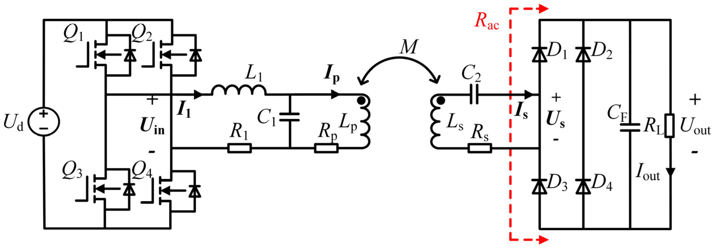
Figure 3.
Simplified circuit diagram of the LC/S compensated IPT system.
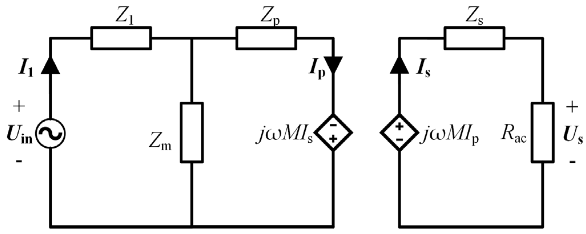
According to Figure 3, the loop equation of the topology should satisfy the following:
where Z1, Zm, Zp, and Zs are equivalent impedances expressed as
I1 is the input current phasor of the topology. Ip and Is represent the current phasors of the transmitting and receiving loops, respectively. According to Formula (2), the expression of the current phasors can be calculated as
where A and B in the denominator can be expressed as
2.2. Analysis of CCO Characteristics and ZPA Operation
Based on the above analysis, when Rac is not included in the expression of Is, CCO characteristics can be realized. It is clear from Formula (4) that if A = 0 holds, Is is independent of Rac, namely
When Equation (6) holds, the input impedance Zin of the proposed system can be expressed as
According to Formula (7), if the following Formula (8) is established, the input impedance Zin is pure resistance, and the ZPA input of the system is realized.
The conditions for satisfying CCO and ZPA input can then be summed up as
When Formula (9) is established, the current expressions can be simplified as
The input impedance Zin and the transconductance gain G can be simplified as
Obviously, according to Formula (11), the input impedance Zin is related only to Rac, so the system input impedance is purely resistive, and ZPA input can be achieved under different loads. According to Formula (12), the transconductance gain G is independent of Rac. Therefore, the proposed system can achieve CCO functions.
2.3. Analysis of CVO Characteristics and ZPA Operation
As in the analysis in the previous section, the output voltage Us can be obtained as
According to Formula (13), when the condition B = 0 is established, the output voltage Us is independent of Rac, and CVO characteristics can be realized, namely
Furthermore, the input impedance Zin of the proposed system can be expressed as
According to Formula (15), if Formula (16) holds, it can be guaranteed that the input impedance Zin has no imaginary part and is related only to Rac, namely, the realization of the ZPA operation.
The conditions for satisfying CVO and ZPA input can then be summed up as
According to the above conditional equations, the input impedance Zin and the voltage gain E can be simplified as
Obviously, according to Formula (18), the input impedance Zin is related only to the equivalent load resistance Rac, so the system can achieve ZPA input under different loads. According to Formula (19), the voltage gain E is not affected by the equivalent load resistance Rac, and therefore the system can realize CVO at the full load.
2.4. Determination of Compensation Capacitor Value
Based on the above analysis, to realize the CCO and CVO characteristics and ZPA operation meeting battery charging requirements, the compensation capacitors C1 and C2 must simultaneously satisfy Equations (9) and (17). Therefore, the expressions of compensation capacitors C1 and C2 can be obtained by associating Equations (3), (9) and (17).
3. Design and Preliminary Verification
The theoretical analysis in Section 2 shows that the proposed LC/S compensated IPT system can realize CCO and CVO characteristics with ZPA operation at fixed operating frequencies. This section describes the structural design of the LCT, providing a strict system parameter design process. In addition, by building an equivalent model, the above theoretical analysis is preliminarily verified.
3.1. LCT Structure Design
LCTs are generally designed with circular, square or rectangular structures. According to [26], square coils have higher mutual and self-inductance than circular coils of the same diameter. Moreover, the mutual inductance of square coils is more stable under horizontal offset, but the current at the corners of the square coils is typically uneven due to collector and proximity effects. To avoid the impact of the corners on the current and reduce loss, a rounded corner design can be selected. Therefore, both the transmitting coil Lp and the receiving coil Ls of the proposed LC/S compensated IPT system adopt a square coil structure with rounded corners. The specific parameters of the coils Lp and Ls are shown in Table 1.
Since there is compensation inductance L1 on the transmitter side, it will generate unnecessary coupling interference with Lp and Ls, which complicates the design and affects the efficiency of system energy transmission. Therefore, this article considers the decoupling design of the series compensation inductor L1 and LCT. According to [27], unipolar coils and bipolar coils placed in parallel have no coupled mutual inductance in case of alignment. Figure 4 shows the magnetic field distribution diagrams generated by unipolar and bipolar coils. B and I in the figure represent the magnetic field and current of the coils respectively. Generally, unipolar coils generate a magnetic field away from the center of the magnetic field, while bipolar coils produce a magnetic field distributed along the axis (long axis or width axis). When the unipolar coil and the bipolar coil are coaxially placed in parallel, since the magnetic flux generated by the bipolar coil is symmetrical along the space, the magnetic flux flowing into the unipolar coil is equal to the magnetic flux flowing out of the bipolar coil. Therefore, the unipolar coil and the bipolar coil are decoupled from each other, i.e., there is no coupled mutual inductance between them. This decoupling design can maximize the space utilization of the magnetic coupling coil, reduce the size of the IPT system, and ensure that the transmitting coil Lp transmits power only to the receiving coil Ls, improving the transmission efficiency and stability of the system.
To verify the correctness of the decoupling design according to the structural parameters in Table 1, a model of the compensation inductance L1 and LCT was created using the electromagnetic simulation software Maxwell, as shown in Figure 5. The compensation inductor L1 uses a bipolar (DD) coil, whereas the coils Lp and Ls employ square unipolar coil structures with rounded corners. Wherein Lp is placed immediately on L1, Ls is positioned directly above Lp, and the three coils are placed coaxially and parallel. The ferrite is placed outside the coil to reduce series impedance and enhance electromagnetic performance. Finally, a simulation analysis is carried out using the electromagnetic field analysis software Maxwell to estimate the self-inductance values of L1, Lp and Ls, as well as the values of Mp1 (mutual inductance between L1 and Lp), Ms1 (mutual inductance between L1 and Ls) and Mps (mutual inductance between Lp and Ls). The simulation results are listed in Table 2. It can be seen from Table 2 that the values of Mp1 and Ms1 are nearly 0, which is an intuitive proof for the design of the above-mentioned decoupling characteristics.
3.2. Parameter Design
This section presents the parameter design steps of the proposed system. A flow chart of the parameter design is depicted in Figure 6.
- Step 1:
- The operating angular frequencies ωcc and ωcv of the proposed system in CC and CV modes are determined in accordance with the specific applications.
- Step 2:
- Determine the appropriate transconductance gain G and voltage gain E.
- Step 3:
- Set the size and turns of L1, Lp and Ls.
- Step 4:
- The self-inductances of L1, Lp and Ls and mutual inductance M are estimated by Maxwell.
- Step 5:
- The compensation capacitances C1 and C2 can be calculated by using Equation (20).
- Step 6:
- Judge whether Equations (9) and (17) are satisfied. If Equations (9) and (17) hold, system parameters are successfully designed. If Equations (9) and (17) are not satisfied, the design parameters are unreasonable. Repeat step 3 until Equations (9) and (17) are hold.
Finally, the theoretical system parameters are summarized in Table 3.
3.3. Preliminary Verification
In this section, the equivalent models of the LC/S compensation IPT system under CC and CV modes are established in MATLAB, and the functions of the system are initially verified. According to the data in Table 2 and Table 3 and the established equivalent model, the relation curve of the system input impedance angle and the transconductance/voltage gains changing with frequency under different loads can be generated. Through the simulation analysis of the equivalent model, Figure 7 and Figure 8 verify that load-independent CCO and CVO can be achieved at two distinct ZPA operating frequency points.
4. Design of Switching Strategy
As was confirmed in the previous section, the proposed LC/S compensated IPT system can achieve CCO and CVO characteristics at two distinct ZPA operating frequencies through appropriate parameter design, without the need for redundant AC switches (ACS). Figure 9 shows the switching strategy for the system charging mode. Figure 10 depicts the mode-switching part in the green box in Figure 9. More specifically, when the IPT system starts to work, the charging voltage Ubat and current Ibat of the battery are synchronously measured by the voltage and current sensors, and the values are sent to the controller. Uset is the charging voltage specified in CV mode, namely, the critical voltage at the transition point (Uset = 45 V) between CC mode and CV mode. When Ubat < Uset, the controller charges in CC mode at the CC frequency fcc. As the voltage continues to rise until Ubat ≥ Uset, the controller charges in CV mode at the CV frequency fcv. As the charging current decreases, the IPT system stops working when the charging current Ibat < Imin is detected. Imin is the specified minimum charging current (Imin = 0.25 A).
5. Experimental
To verify the above theory, a confirmatory experimental prototype of the proposed system was constructed. The hardware of the prototype is shown in Figure 11. It consists of a DC voltage source, a compensation inductor L1, compensation capacitors C1 and C2, an LCT, an HFI, a rectifier, a resistive load, and an oscilloscope. Referring to the LCT structural parameters in Table 2, the coil used for the experiment is wound, as illustrated in Figure 12. As shown in Figure 12, the transmitting coil Lp is placed just above the series compensation inductor L1, ensuring the compactness of the whole IPT system. In addition, the coupling mutual inductances between Lp and L1 and between Ls and L1 are both zero as measured by the LCR meter, which verifies the theoretical analysis of the decoupling coil in Section 3. The measured values for each piece of hardware are shown in Table 4.
Figure 13 displays the waveforms of Uin, I1, Iout and Uout at an operating frequency of 90 kHz when the loads are 10 Ω and 15 Ω, respectively. According to Figure 13, Uin and I1 are always in phase under different loads. In addition, Iout remains at 2.5 A, which means that ZPA operation and CCO are realized. Figure 14 displays the experimental waveforms of Uin, I1, Iout and Uout at an operating frequency of 72 kHz when the loads are 25 Ω and 50 Ω, respectively. Consistent with the above analysis, according to Figure 14, when the operating frequency is 72 kHz, the system can achieve CVO with ZPA operation. In summary, it is verified by experiments that the LC/S compensated IPT system proposed in this study can realize CCO and CVO characteristics at fixed ZPA operating frequency points. Therefore, the charging requirements of the battery are satisfied.
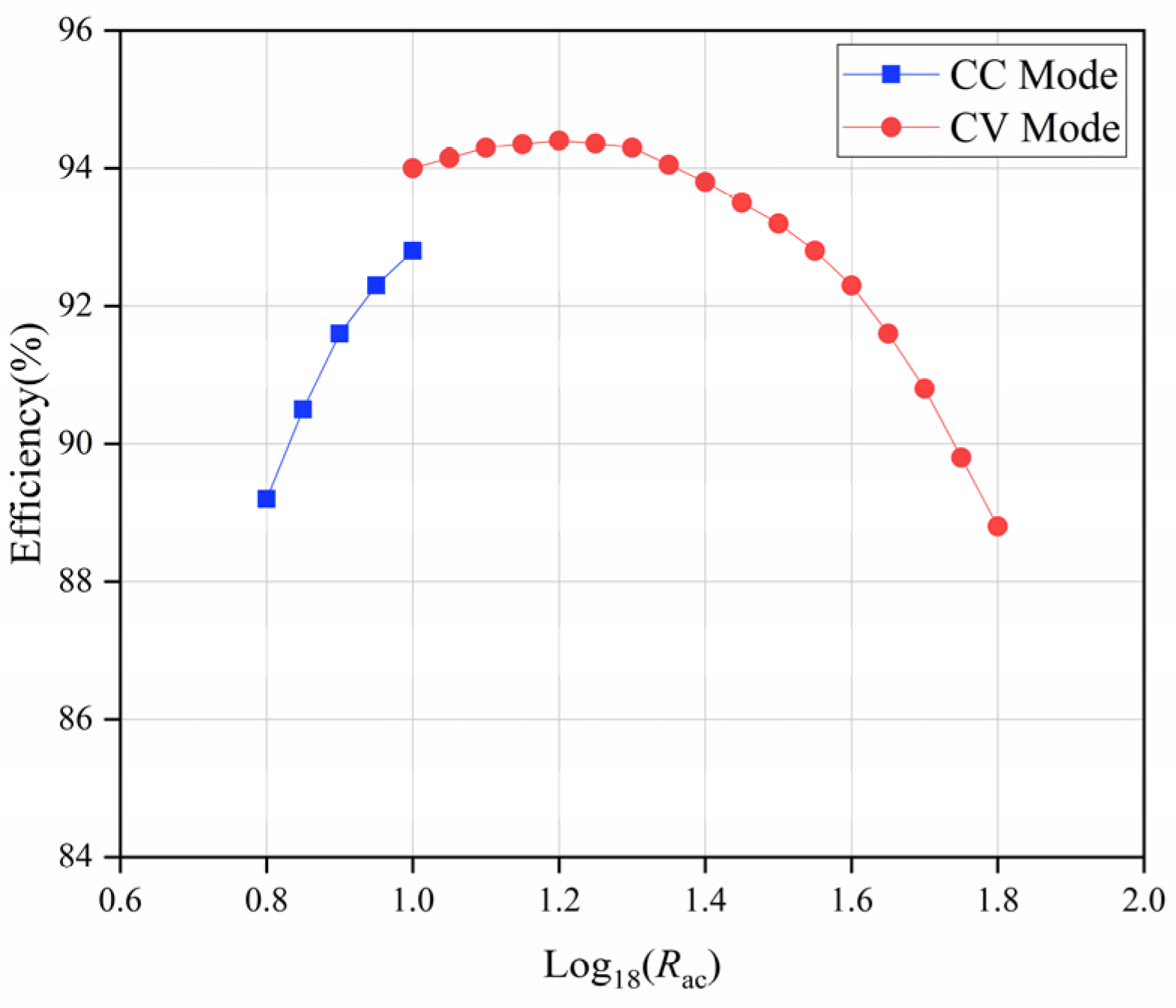
The energy transmission efficiency curve of the system during the whole charging process is displayed in Figure 15. In CC charging mode, the energy transfer efficiency of the system increases rapidly from 89.2% to 92.8%. When the equivalent load rises to 18 Ω, the operating frequency of the system is switched from ωcc to ωcv for CV charging mode. In CV charging mode, the peak energy transfer efficiency of the system is 94.4%. In addition, the power transfer efficiency of the system stays at a relatively high level throughout the charging process, which ensures high efficiency of the proposed LC/S compensated IPT system.
To illustrate the advantages of the proposed LC/S compensated IPT system, a summary is given below:
- (i)
- The proposed LC/S compensated IPT system does not require redundant AC switches and complex control algorithms, and shifts between two fixed operating frequencies to realize CCO and CVO with ZPA operation, which not only makes the system simpler in structure, but also makes control of the system more convenient. In addition, the total number of compensation elements of the system is minimized, with only one compensation capacitor on the receiving side, ensuring a compact and low-cost receiver.
- (ii)
- The proposed LC/S compensated IPT system adopts a coil decoupling design, which eliminates the coupling mutual inductance between the compensation inductor L1 and the LCT, maximizing space utilization.
6. Conclusions
To satisfy the charging requirements of the battery first in the CC stage and later in the CV stage, this article proposed an IPT system based on LC/S compensation. The system enables full-load-range ZPA operation as well as load-independent CCO and CVO at distinct operating frequencies. The detailed circuit analysis and parameter design process of the proposed system are provided in this article, and experiments verify its output characteristics. Notably, the series compensation inductor is designed as a DD structure to eliminate coupling interference between the inductor and the LCT, which not only reduces the complexity of system parameter design, but also reduces the space used by the magnetic coupling coil. Moreover, the total number of compensation elements of the system is minimized, with only one compensation capacitor on the receiving side, which not only ensures the low cost of the system but also makes the receiver more compact.
Author Contributions
Conceptualization, X.Z. and S.S.; methodology, X.Z.; software, S.S.; validation, X.Z., S.S. and Y.T.; formal analysis, Y.T.; investigation, A.C.; resources, X.Z. and L.Y.; data curation, Z.W.; writing—original draft preparation, S.S.; writing—review and editing, X.Z. and L.Y.; visualization, Y.T.; supervision, X.Z.; funding acquisition, X.Z. All authors have read and agreed to the published version of the manuscript.
Funding
This research was funded in part by a Scientific Research Project of the Hunan Provincial Department of Education (22B0803), and in part by the Yongzhou 2022 Guiding Science and Technology Plan Project (2022-YZKJZD-010).
Institutional Review Board Statement
Not applicable.
Informed Consent Statement
Not applicable.
Data Availability Statement
Not applicable.
Conflicts of Interest
The authors declare no conflict of interest.
References
- Hui, S.Y. Planar Wireless Charging Technology for Portable Electronic Products and Qi. Proc. IEEE 2013, 101, 1290–1301. [Google Scholar] [CrossRef] [Green Version]
- Feng, J.; Li, Q.; Lee, F.C.; Fu, M. Transmitter Coils Design for Free-Positioning Omnidirectional Wireless Power Transfer System. IEEE Trans. Ind. Inform. 2019, 15, 4656–4664. [Google Scholar] [CrossRef]
- Li, Y.; Hu, J.; Li, X.; Chen, F.; Xu, Q.; Mai, R.; He, Z. Analysis, Design, and Experimental Verification of a Mixed High-Order Compensations-Based WPT System with Constant Current Outputs for Driving Multistring LEDs. IEEE Trans. Ind. Electron. 2020, 67, 203–213. [Google Scholar] [CrossRef]
- Xiaohui, Q.; Wei, Z.; Siu-Chung, W.; Tse, C.K. Design of a Current-Source-Output Inductive Power Transfer LED Lighting System. IEEE J. Emerg. Sel. Top. Power Electron. 2015, 3, 306–314. [Google Scholar] [CrossRef]
- Agarwal, K.; Jegadeesan, R.; Guo, Y.X.; Thakor, N.V. Wireless Power Transfer Strategies for Implantable Bioelectronics. IEEE Rev. Biomed Eng. 2017, 10, 136–161. [Google Scholar] [CrossRef]
- Pucci, N.; Kwan, C.H.; Yates, D.C.; Mitcheson, P.D. Multi-megahertz IPT systems for biomedical devices applications. In Proceedings of the 2019 19th International Conference on Micro and Nanotechnology for Power Generation and Energy Conversion Applications (PowerMEMS), Krakow, Poland, 2–6 December 2019; pp. 1–7. [Google Scholar]
- Cai, C.; Wang, J. A cost-effective segmented dynamic wireless charging system with stable efficiency and output power. IEEE Trans. Power Electron. 2022, 37, 8682–8700. [Google Scholar] [CrossRef]
- Yang, L.; Shi, Y.; Wang, M. Constant voltage charging and maximum efficiency tracking for WPT systems employing dual-side control scheme. IEEE J. Emerg. Sel. Top. Power Electron. 2021, 10, 945–955. [Google Scholar] [CrossRef]
- Cai, C.; Wang, J.; Zhang, F.; Liu, X.; Zhang, P.; Zhou, Y.-G. A Multichannel Wireless UAV Charging System With Compact Receivers for Improving Transmission Stability and Capacity. IEEE Syst. J. 2022, 16, 997–1008. [Google Scholar] [CrossRef]
- Wang, J.; Chen, R.; Cai, C.; Zhang, J.; Wang, C. An Onboard Magnetic Integration Based WPT System for UAV Misalignment-Tolerant Charging with Constant Current Output. IEEE Trans. Transp. Electrif. 2022, 9, 1973–1984. [Google Scholar] [CrossRef]
- Mohsan, S.A.H.; Islam, A.; Khan, M.A.; Mahmood, A.; Rokia, L.S.; Mazinani, A.; Amjad, H. A Review on Research Challenges, Limitations and Practical Solutions for Underwater Wireless Power Transfer. Int. J. Adv. Comput. Sci. Appl. 2020, 11, 555–562. [Google Scholar] [CrossRef]
- Khaligh, A.; Zhihao, L. Battery, Ultracapacitor, Fuel Cell, and Hybrid Energy Storage Systems for Electric, Hybrid Electric, Fuel Cell, and Plug-In Hybrid Electric Vehicles: State of the Art. IEEE Trans. Veh. Technol. 2010, 59, 2806–2814. [Google Scholar] [CrossRef]
- Qu, X.; Han, H.; Wong, S.-C.; Tse, C.K.; Chen, W. Hybrid IPT Topologies with Constant Current or Constant Voltage Output for Battery Charging Applications. IEEE Trans. Power Electron. 2015, 30, 6329–6337. [Google Scholar] [CrossRef]
- Wei, Z.; Siu-Chung, W.; Tse, C.K.; Qianhong, C. Load-Independent Duality of Current and Voltage Outputs of a Series- or Parallel-Compensated Inductive Power Transfer Converter with Optimized Efficiency. IEEE J. Emerg. Sel. Top. Power Electron. 2015, 3, 137–146. [Google Scholar] [CrossRef]
- Zhang, W.; Mi, C.C. Compensation Topologies of High-Power Wireless Power Transfer Systems. IEEE Trans. Veh. Technol. 2016, 65, 4768–4778. [Google Scholar] [CrossRef]
- Mai, R.; Chen, Y.; Li, Y.; Zhang, Y.; Cao, G.; He, Z. Inductive Power Transfer for Massive Electric Bicycles Charging Based on Hybrid Topology Switching with a Single Inverter. IEEE Trans. Power Electron. 2017, 32, 5897–5906. [Google Scholar] [CrossRef]
- Liu, S.; Li, X.; Yang, L. Three-coil structure-based WPT system design for electric bike CC and CV charging without communication. IET Electr. Power Appl. 2019, 13, 1318–1327. [Google Scholar] [CrossRef]
- Chen, Y.; Li, M.; Yang, B.; Chen, S.; Li, Q.; He, Z.; Mai, R. Variable-Parameter T-Circuit-Based IPT System Charging Battery with Constant Current or Constant Voltage Output. IEEE Trans. Power Electron. 2020, 35, 1672–1684. [Google Scholar] [CrossRef]
- Chen, Y.; Yang, N.; Yang, B.; Dai, R.; He, Z.; Mai, R.; Gao, S. Two-/three-coil hybrid topology and coil design for WPT system charging electric bicycles. IET Power Electron. 2019, 12, 2501–2512. [Google Scholar] [CrossRef]
- Huang, Z.; Wong, S.-C.; Tse, C.K. Design of a Single-Stage Inductive-Power-Transfer Converter for Efficient EV Battery Charging. IEEE Trans. Veh. Technol. 2017, 66, 5808–5821. [Google Scholar] [CrossRef]
- Yang, L.; Ren, L.; Shi, Y.; Wang, M.; Geng, Z. Analysis and Design of a S/S/P-Compensated Three-coil Structure WPT System with Constant Current and Constant Voltage Output. IEEE J. Emerg. Sel. Top. Power Electron. 2022, 1-1. [Google Scholar] [CrossRef]
- Vu, V.-B.; Tran, D.-H.; Choi, W. Implementation of the Constant Current and Constant Voltage Charge of Inductive Power Transfer Systems with the Double-Sided LCC Compensation Topology for Electric Vehicle Battery Charge Applications. IEEE Trans. Power Electron. 2018, 33, 7398–7410. [Google Scholar] [CrossRef] [Green Version]
- Yang, L.; Li, X.; Liu, S.; Xu, Z.; Cai, C.; Guo, P. Analysis and Design of Three-Coil Structure WPT System with Constant Output Current and Voltage for Battery Charging Applications. IEEE Access 2019, 7, 87334–87344. [Google Scholar] [CrossRef]
- Tran, D.H.; Vu, V.B.; Choi, W. Design of a High-Efficiency Wireless Power Transfer System with Intermediate Coils for the On-Board Chargers of Electric Vehicles. IEEE Trans. Power Electron. 2018, 33, 175–187. [Google Scholar] [CrossRef]
- Yang, L.; Jiang, S.; Wang, C.; Zhang, L. Analysis and Design of a CLC/N Compensated CC-Type WPT System with Compact and Low-Cost Receiver. Sensors 2023, 23, 838. [Google Scholar] [CrossRef]
- Cai, C.; Wang, J.; Fang, Z.; Zhang, P.; Hu, M.; Zhang, J.; Li, L.; Lin, Z. Design and Optimization of Load-Independent Magnetic Resonant Wireless Charging System for Electric Vehicles. IEEE Access 2018, 6, 17264–17274. [Google Scholar] [CrossRef]
- Li, Y.; Lin, T.; Mai, R.; Huang, L.; He, Z. Compact Double-Sided Decoupled Coils-Based WPT Systems for High-Power Applications: Analysis, Design, and Experimental Verification. IEEE Trans. Transp. Electrif. 2018, 4, 64–75. [Google Scholar] [CrossRef]
Figure 1.
Lithium-ion battery charging curve.

Figure 4.
The magnetic field distribution diagram of the coils: (a) unipolar coil topology; (b) bipolar coil topology.
Figure 4.
The magnetic field distribution diagram of the coils: (a) unipolar coil topology; (b) bipolar coil topology.
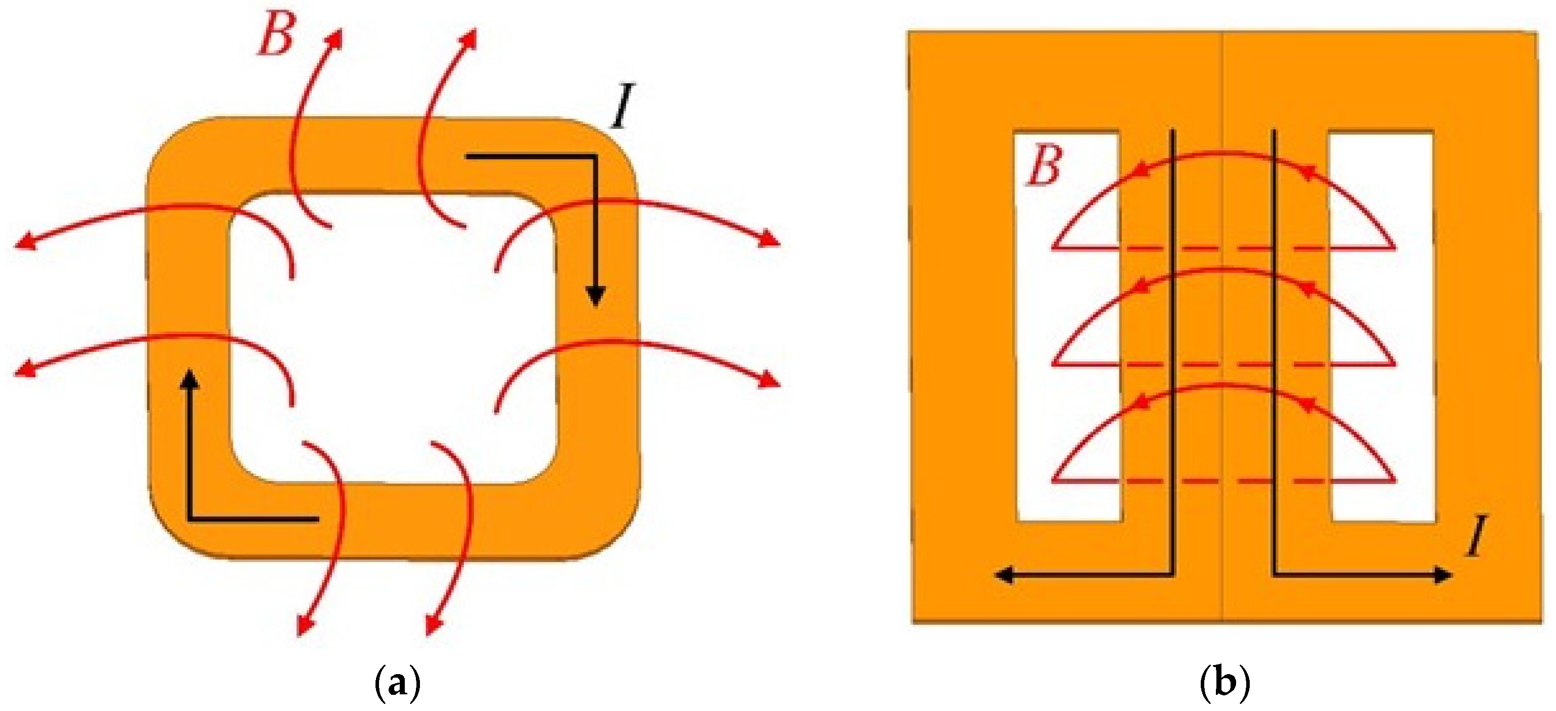
Figure 5.
3D model of the LCT.
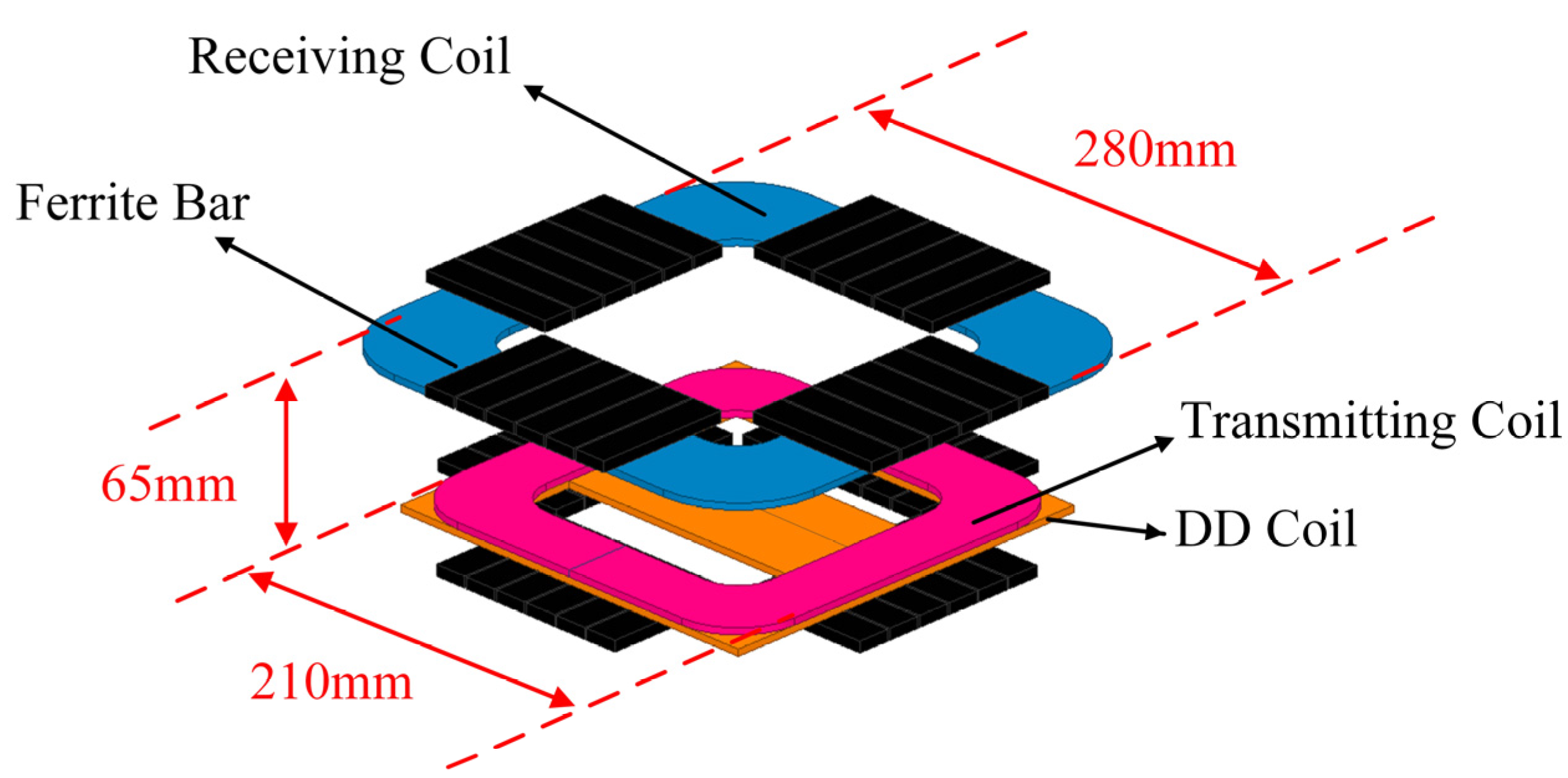
Figure 6.
Design approach of the proposed LC/S compensated IPT system.

Figure 7.
Transconductance gain and input impedance angle of the proposed LC/S compensated IPT system. (a) Input Impedance Angle; (b) Transconductance gain.
Figure 7.
Transconductance gain and input impedance angle of the proposed LC/S compensated IPT system. (a) Input Impedance Angle; (b) Transconductance gain.
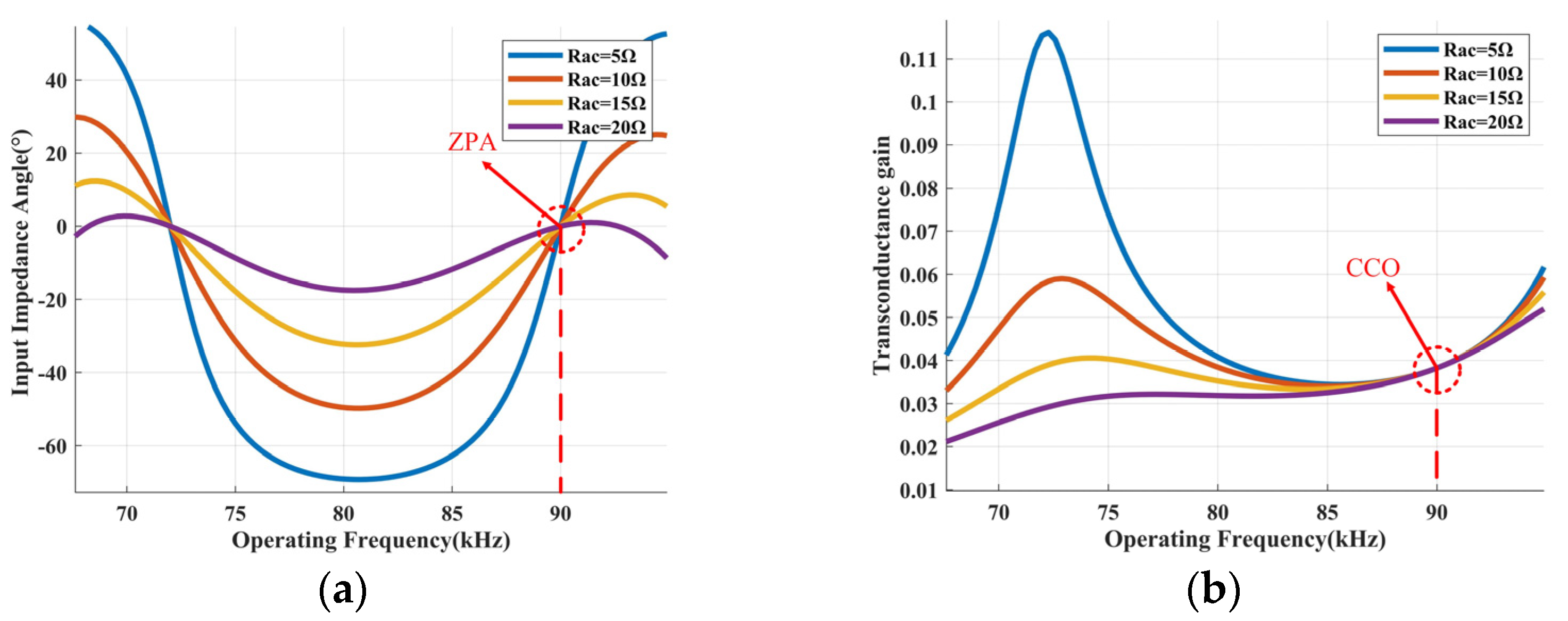
Figure 8.
Voltage gain and input impedance angle of the proposed LC/S compensated IPT system. (a) Input Impedance Angle; (b) Voltage gain.
Figure 8.
Voltage gain and input impedance angle of the proposed LC/S compensated IPT system. (a) Input Impedance Angle; (b) Voltage gain.
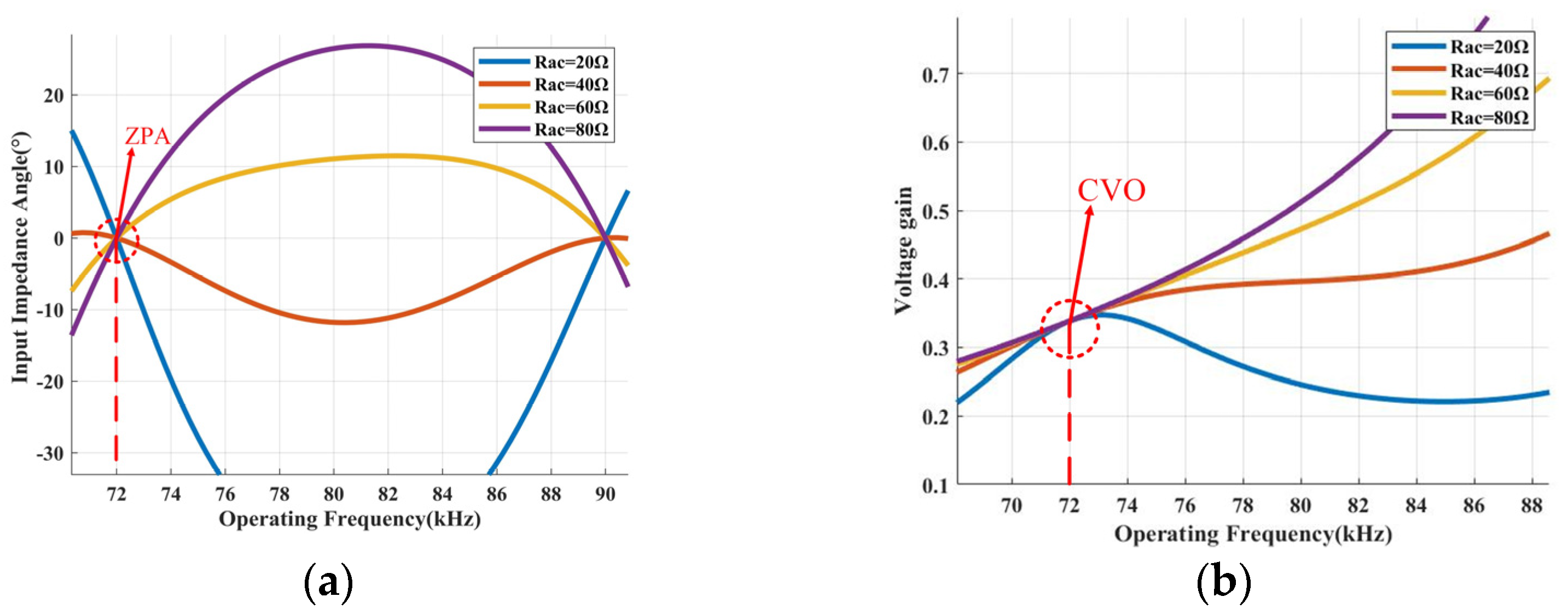
Figure 9.
Switching strategy for the proposed LC/S compensated IPT system.
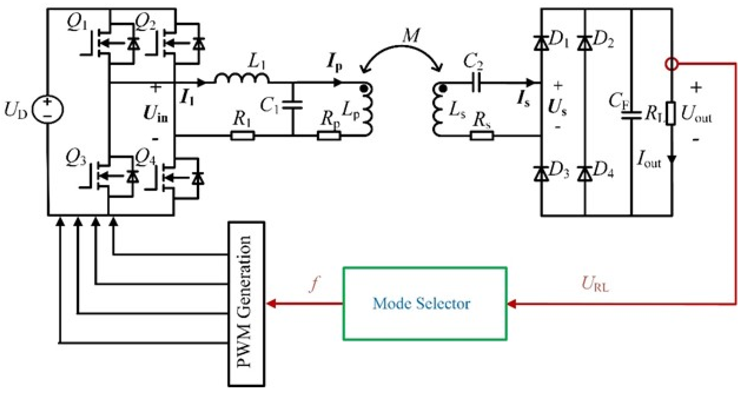
Figure 10.
Program diagram for mode selection.
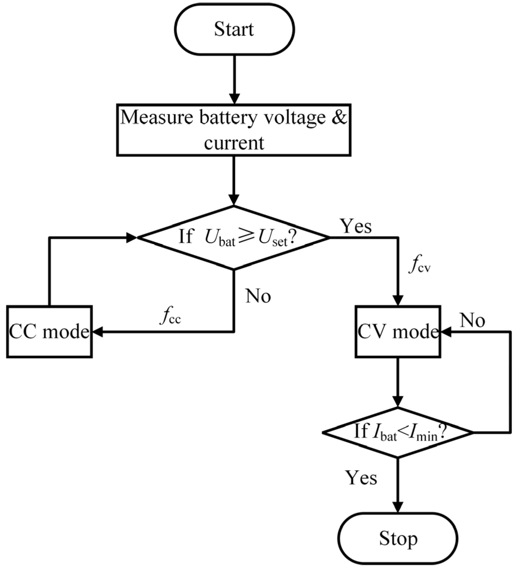
Figure 11.
Experimental setup of the proposed LC/S compensated IPT system.
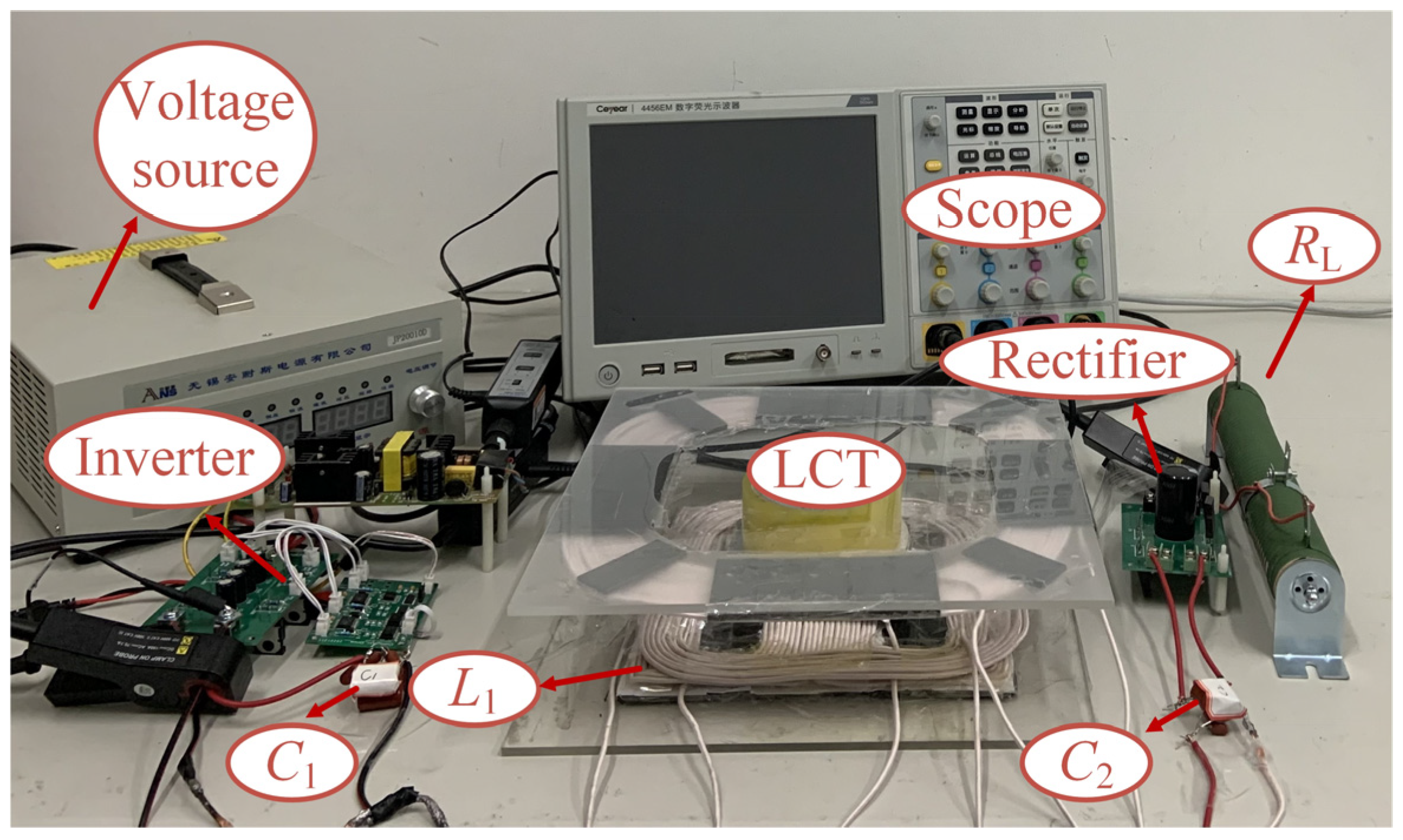
Figure 12.
Experimental setup of the proposed LC/S compensated IPT system: (a) transmitting pad, (b) receiving pad.
Figure 12.
Experimental setup of the proposed LC/S compensated IPT system: (a) transmitting pad, (b) receiving pad.

Figure 13.
Experimental waveforms of the IPT system in CC charging mode. (a) RL = 10 Ω; (b) RL = 15 Ω.
Figure 13.
Experimental waveforms of the IPT system in CC charging mode. (a) RL = 10 Ω; (b) RL = 15 Ω.

Figure 14.
Experimental waveforms of the IPT system in CV charging mode. (a) RL = 25 Ω; (b) RL = 50 Ω.
Figure 14.
Experimental waveforms of the IPT system in CV charging mode. (a) RL = 25 Ω; (b) RL = 50 Ω.
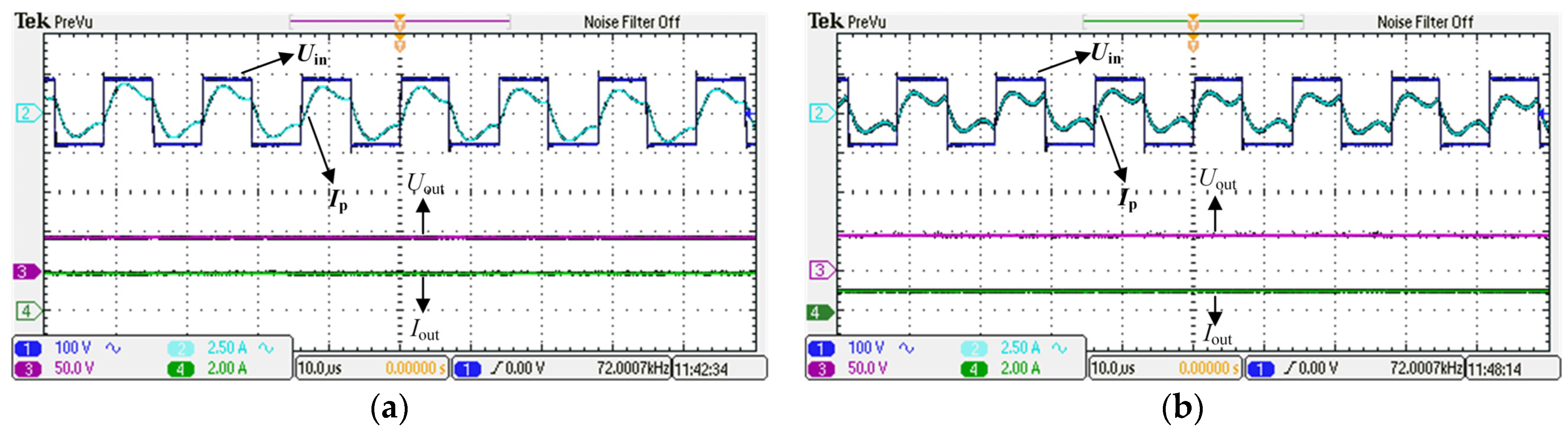
Figure 15.
The efficiency of the proposed LC/S compensated IPT system throughout the charging process.
Figure 15.
The efficiency of the proposed LC/S compensated IPT system throughout the charging process.

Table 1.
Dimensional parameters of the designed LCT.
| Parameters | Transmitting Coil Lp | Receiving Coil Ls |
|---|---|---|
| Outer diameter | 210 mm | 280 mm |
| Internal diameter | 156 mm | 196 mm |
| Turns of coils (n) | 9 | 14 |
| Specifications of Litz wire | 400 strands | 400 strands |
Table 2.
Simulation values for compensation inductance and LCT.
| Parameters | Value | Parameters | Value |
|---|---|---|---|
| L1 | 80 | Mp1 | 1.21 |
| Lp | 45 | Ms1 | 0.26 |
| Ls | 136.68 | Mps | 26 |
Table 3.
Design values of crucial parameters in the proposed LC/S compensated IPT system.
| Parameters | Value | Parameters | Value |
|---|---|---|---|
| fcc | 90 kHz | C1 | 108.58 nF |
| fcv | 72 kHz | C2 | 32.93 nF |
Table 4.
Measured values of specific parameters in the proposed LC/S compensated IPT system.
| Parameters | Value | Parameters | Value |
|---|---|---|---|
| fcc | 90 kHz | C1 | 107.73 nF |
| fcv | 72 kHz | C2 | 32.61 nF |
| L1 | Rp | 0.12 Ω | |
| Lp | Rs | 0.08 Ω | |
| Ls | Rm | 0.16 Ω | |
| M | Iout | 2.5 A | |
| Ud | 82 V | Uout | 45 V |
Disclaimer/Publisher’s Note: The statements, opinions and data contained in all publications are solely those of the individual author(s) and contributor(s) and not of MDPI and/or the editor(s). MDPI and/or the editor(s) disclaim responsibility for any injury to people or property resulting from any ideas, methods, instructions or products referred to in the content. |
© 2023 by the authors. Licensee MDPI, Basel, Switzerland. This article is an open access article distributed under the terms and conditions of the Creative Commons Attribution (CC BY) license (https://creativecommons.org/licenses/by/4.0/).
Share and Cite
MDPI and ACS Style
Zhou, X.; Shao, S.; Tan, Y.; Chen, A.; Wang, Z.; Yang, L. Design and Implementation of an IPT Charger with Minimum Number of Elements for Battery Charging Applications. Appl. Sci. 2023, 13, 3580. https://doi.org/10.3390/app13063580
AMA Style
Zhou X, Shao S, Tan Y, Chen A, Wang Z, Yang L. Design and Implementation of an IPT Charger with Minimum Number of Elements for Battery Charging Applications. Applied Sciences. 2023; 13(6):3580. https://doi.org/10.3390/app13063580
Chicago/Turabian StyleZhou, Xuebin, Shuai Shao, Yonghong Tan, Aiwu Chen, Zhitang Wang, and Lin Yang. 2023. "Design and Implementation of an IPT Charger with Minimum Number of Elements for Battery Charging Applications" Applied Sciences 13, no. 6: 3580. https://doi.org/10.3390/app13063580
Note that from the first issue of 2016, this journal uses article numbers instead of page numbers. See further details here.