Article

Assessment of the Development Performance of Additive Manufacturing VPP Parts Using Digital Light Processing (DLP) and Liquid Crystal Display (LCD) Technologies

by
Moises Batista
1,*,
Jairo Mora-Jimenez
1,
Jorge Salguero
1 and
Juan Manuel Vazquez-Martinez
2,*
1
Mechanical Engineering and Industrial Design Department, School of Engineering, University of Cadiz, Avda. de la Universidad de Cadiz, 10, E11519 Puerto Real, Spain
2
Industrial Engineering and Civil Engineering Department, Polytechnic School of Engineering of Algeciras, Avda. Ramón Puyol, s/n, E11202 Algeciras, Spain
*
Authors to whom correspondence should be addressed.
Appl. Sci. 2024, 14(9), 3607; https://doi.org/10.3390/app14093607
Submission received: 7 April 2024 / Revised: 18 April 2024 / Accepted: 19 April 2024 / Published: 24 April 2024
(This article belongs to the Special Issue Recent Advances in 3D Printing and Additive Manufacturing Technology)

Abstract

:
Non-metallic additive manufacturing technology has seen a substantial improvement in the precision of the parts it produces. Its capability to achieve complex geometries and very small dimensions makes it suitable for integration into strategic industrial sectors, such as aeronautics and medicine. Among additive manufacturing technologies, resin development processes demonstrate enhanced precision when compared to other methods, like filament printing. This study conducts a comparative analysis between digital light processing (DLP) and liquid crystal display (LCD) photopolymerization processes to assess the performance of the technologies and how process parameters affect the accuracy of the resulting parts. The research evaluates the impact of the discretization process used during the digital model export, determining the optimal mesh size and then analyzing the geometric deviations that occur by altering various operating parameters of the process. Statistical methods will be employed to identify the most significant parameters in the manufacturing process. Among other aspects, the precision of manufacturing technologies regarding the movement axis has also been evaluated. Regarding the minimum size of the features that can be fabricated, DLP technology has surpassed LCD technology, successfully producing features as small as 200 µm, compared to 500 µm for LCD technology.

1. Introduction

Additive manufacturing (AM) has generated increasing interest in recent years and is currently undergoing tremendous development. The possibility of creating customised and complex parts in a relatively short time makes AM a very interesting manufacturing process on an industrial level. Therefore, this technology serves as a complement and extension of conventional subtractive manufacturing technologies [1,2,3]. More and more companies are using this technology in their production processes, as in many cases, it considerably reduces costs and times compared to those of other conventional manufacturing techniques [4,5,6,7,8,9].
Despite these advantages, AM, compared to other manufacturing processes, is a very recent technology and in certain aspects, still requires further maturity. The main technological challenge is still to improve the ability to obtain parts that are functional and can be used in industrial sectors [10]. This is why the technology is constantly evolving. This can be seen in the efforts made in recent years to develop specific regulations for implementing AM as a general manufacturing process [6,11]. Although it should be noted that in certain aspects, such as metrology, this technology still lags far behind the development of other more consolidated processes.
AM is very useful when low production volumes, high design complexity, and frequent design changes are required, as it offers the possibility of producing complex parts, overcoming the design limitations of traditional manufacturing methods [5,7] and becoming a highly virtualised process. For this reason, the starting point of any AM process is considered to be the design of the part to be manufactured, from which a geometric information exchange model is obtained. One of the most widely used interchange formats in AM is STL (Standard Tessellation Language), developed in 1986 together with the stereolithography and has since become a standard, although there are formats that offer more features, such as the AMF (additive manufacturing file) format [12,13]. The STL format performs a decomposition of the modelled surface geometry by discretising it into flat tessellated triangles that share their edges to form a mesh [14].
In this way, an approximation is made to the designed model and if the goal is to reduce the approximation error committed when discretising the model, the density of the facets or faces of the mesh is increased. This increases the resolution of the mesh, although this entails an increase in the information contained in the file and therefore, an increase in the file’s post-processing time. Therefore, the meshing process must be optimised to improve processing times [12,13,14,15]. This is very important in the case of AM, as a non-optimised STL file can lead to increased pre-processing time or geometric errors in the final parts caused by approximation errors.
Although this effect will be more determinant in those AM processes in which a high quality of the parts is sought or in those where it is possible to obtain more precise details, as in the case of VAT photopolymerisation processes. In these processes, a liquid photopolymer is selectively cured inside a tank by the action of a light source, usually ultraviolet, which activates polymerisation [13,16]. When the resin is exposed to the curing light, photoinitiators release species that act as catalysts for the formation of chains between monomers and oligomers. The chemical–thermal process of chain formation is irreversible, and the prototypes cannot return to their liquid form. Using this principle, consecutive layers of resin are gradually fabricated from a 3D model [17].
The low layer thicknesses used in this process, together with the high lateral accuracies, make it one of the polymer AM processes from which the highest quality is obtained [18,19]. In recent years, the use of this technology has undergone a major expansion, with the number of studies carried out on this process doubling. This has resulted from the increase in low-cost light sources such as UV LCD (liquid crystal display) screens or UV DLP (digital light processing) projectors that allow a complete layer to be cured simultaneously, without the need to scan the photopolymer point by point, as in stereolithography (SLA), making it a much faster manufacturing system [20,21].
In the case of DLP, the curing process of each layer is performed by projecting a specific section of the layer onto the resin surface, which solidifies due to the photon-activated photochemical reaction. After curing of each layer, the platform is moved upwards, and another section view is projected onto the resin for curing, forming the additional layers. The light distribution and intensity of the light is arbitrarily modulated, as light exposure time is required to cure the resin [22]. Due to the high precision of the process, it is suitable for many applications in the medical and healthcare fields [23,24,25,26]. DLP technology has been widely used for microfabrication applications reaching micrometre accuracies [27,28,29]. Several studies have been carried out to observe the accuracy limits offered by this technology, including the study of microstructured surfaces [30,31].
LCD, on the other hand, is based on the use of LCD screens as a system for generating images of the sections of the part to be manufactured. LCD screens allow UV light to pass through their panels so that it can reach the resin directly, and the corresponding layer of the material is cured. This prevents the light from expanding, and therefore, pixel distortion is less of a problem in this technique compared to that noted for DLP manufacturing. However, the quality is a priori inferior, so efforts are being made to improve this system by using screens with better resolution and light transmission, which improve the efficiency of the system [32]. On the other hand, the low cost of LCD displays makes it a highly interesting process [33].
However, there are limitations in these techniques that must be overcome, such as the force required to separate the cured layer and the transparent film from the tank, since during light-curing, the part remains adhered to the film and can suffer deformations [34,35,36,37]. Another important limitation is the material reloading rate, which is the amount of material that fills the gap in the light-cured resin when it separates from the film. This gap must be filled under vacuum, which can lead to incomplete fills, pores, or cracks [34,38,39,40]. This filling time is directly related to the viscosity of the resin, the size of the part, the pressure gradient, the space between the cured part and the interface, and the part geometry [41,42]. It is therefore necessary to optimise the reloading time to obtain defect-free parts. In addition to these limitations, it is necessary to optimise the operating parameters of the process to achieve adequate light curing.
In this study, a comparison is made between the DLP and LCD VAT photopolymerisation processes (VPP), with the intention of analysing the limits of the technology and how the operating parameters of the process can affect the final result of the parts obtained.
We will begin by studying the influence of the discretisation process carried out when exporting the model, establishing the most suitable mesh size and subsequently, analysing the geometric deviations obtained by modifying the different operating parameters of the process. Statistical evaluations will be carried out in order to analyse the influence of the different operational factors, as well as of the technology itself.

2. Materials and Methods

This article compares DLP and LCD manufacturing techniques using VPP technology.
The two devices used are the Photon Ultra, which uses DLP technology, and the Photon S, which uses LCD technology, both from Anycubic (Anycubic, Kowloon, Hong Kong). In the case of the Photon Ultra, it is the first desktop unit to be marketed with this technology. The Photon S uses a high resolution (FHD) LCD screen as part of the projection system. Table 1 shows the general characteristics of both devices. These devices have been selected because they are mid-range devices with similar characteristics and the same manufacturer, so that the comparison is based exclusively on the technology as a differentiating element.
The same concept has been followed in the choice of material. In this case, the premium resin from Copymaster 3D in dark grey was used. This resin has intermediate characteristics, it is water washable, which facilitates cleaning, and is suitable for both devices, as it can be used in equipment operating at a wavelength between 395–405 nm as a light source.
At the end of the fabrication of the parts, they will be subjected to the post-processing process, which includes the washing of the part and the UV post-polymerisation treatment. This process will be carried out in a system from same manufacturer as the initial equipment.
Subsequently, the parts obtained will be analysed using a Nikon SMZ 800 (Nikon, Tokyo, Japan) stereo optical microscope. After calibration of the equipment, the images will be processed and digitally measured in order to obtain the geometric deviation data of the different specimens designed.
This process will be applied to three types of samples in order to analyse the differences between the precision of the technologies and the influence of the operating parameters of the process. As previously mentioned, the creation of the STL file and the mesh it contains is of great importance in an AM process where high quality is sought. In order to observe the influence of the STL mesh resolution on the manufacturing process of a part, a test part, which includes four different hemispheres, each with a different resolution, has been designed. In addition, five different sizes have been produced for each of the resolutions with the aim of examining the minimum size at which the mesh resolution no longer influences the constructed part. The choice of spherical geometries is based on the difficulty of discretisation processes to approximate this type of geometry by means of triangles. For this reason, hemispherical parts will be manufactured in which both the radius of the hemisphere and its export resolution will be varied (Figure 1). This analysis will be used to study the influence of meshing on the final quality of the parts obtained.
Subsequently, a part with a positive geometry (shaft) and a negative geometry (hole), with a square-based prism, will be manufactured (Figure 2). This part will be used to study the deviations that appear in the X and Y axes by modifying different operating parameters of the process.
In the specific case of this study, a factorial design of experiment (DOE), with three factors, was carried out to evaluate the geometric characteristics of the different parts obtained. The three factors taken into account for this experiment are: exposure time, direction of the geometry, and machine used.
In the case of exposure time, three different levels have been considered (1, 2, and 3). These levels correspond to different exposure times that vary according to the technology used, based on the time recommended by the manufacturer. In the DLP process, the exposure times are 1.5, 2, and 2.5 s, and for LCD, the exposure times are 6, 7, and 8 s (Table 2). On the other hand, the geometry direction factor consists of two levels: female, defined as a gap, or male, defined as an axis (Table 2). The last factor that has been assessed in the experiment is the technology used in the manufacture, which, as mentioned above, would be DLP or LCD.
Furthermore, in order to obtain sufficient data to carry out the statistical study and to evaluate the repeatability of the manufacturing process, 6 repetitions of each case have been carried out, resulting in 72 repetitions for the designed geometry.
In order to observe the influence of the factors mentioned in this study, in the specific case of this experiment, the perimeter has been taken as the response variable, since the shape of the pieces is designed so that they can fit together hollow–axis, and this depends, to a large extent, on the perimeter measured in each of the pieces.
The third type of the pieces consist of a pyramid with a cylindrical base where the different steps have been designed with the same height, but different sizes (Figure 3). All of the previous studies focused mainly on the analysis of the geometric characteristics of the parts, oriented towards the horizontal resolution of the manufacturing equipment used. However, it is also important to analyse the vertical resolution of the machines. For this reason, the part has been designed in the form of a stepped pyramid, with a circular base (Figure 3).
Each pyramid consists of 16 steps, with a height of 200 µm for each step, i.e., the total height of the pyramid, with respect to the base, is 3.2 mm. On the other hand, the diameter of the base ranges from 3 mm to 100 µm.
The study consisted of evaluating the heights of all the steps of each piece obtained. Three repetitions of each piece were carried out for each technology. In order to evaluate the differences between the two technologies, the heights of the different steps were measured to see if they were close to the design values, establishing the standard deviation of the data.

3. Results

The interest in the use of additive manufacturing in various application fields has been based on the resolution, manufacturing quality, and manufacturing speed in order to compare this process with other conventional manufacturing techniques [43,44]. Therefore, an increasing amount of research is focused on improving manufacturing speed for the process itself, as well as on the scalability or mass production capability, known as mass customisation [19,45,46]. Therefore, this study will analyse the deviations when processing the model and the deviations that appear when manufacturing the model.

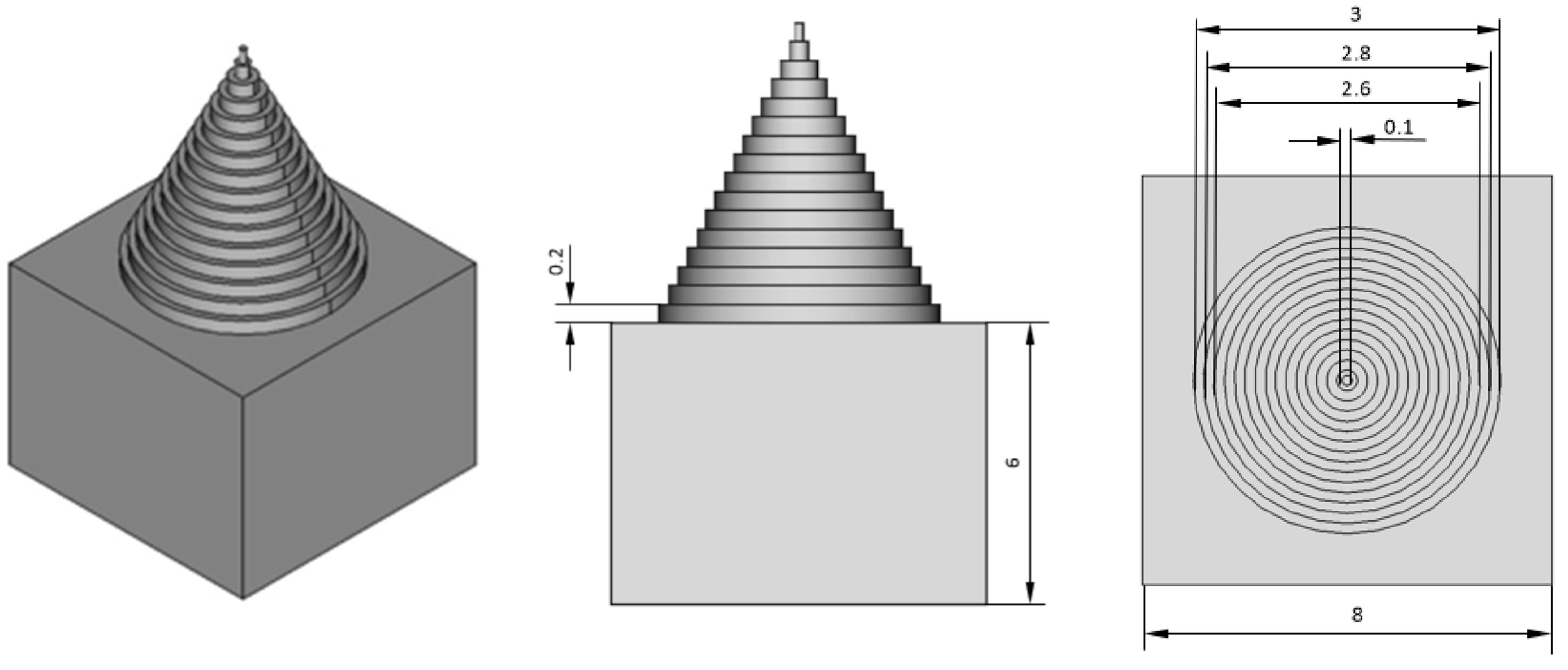
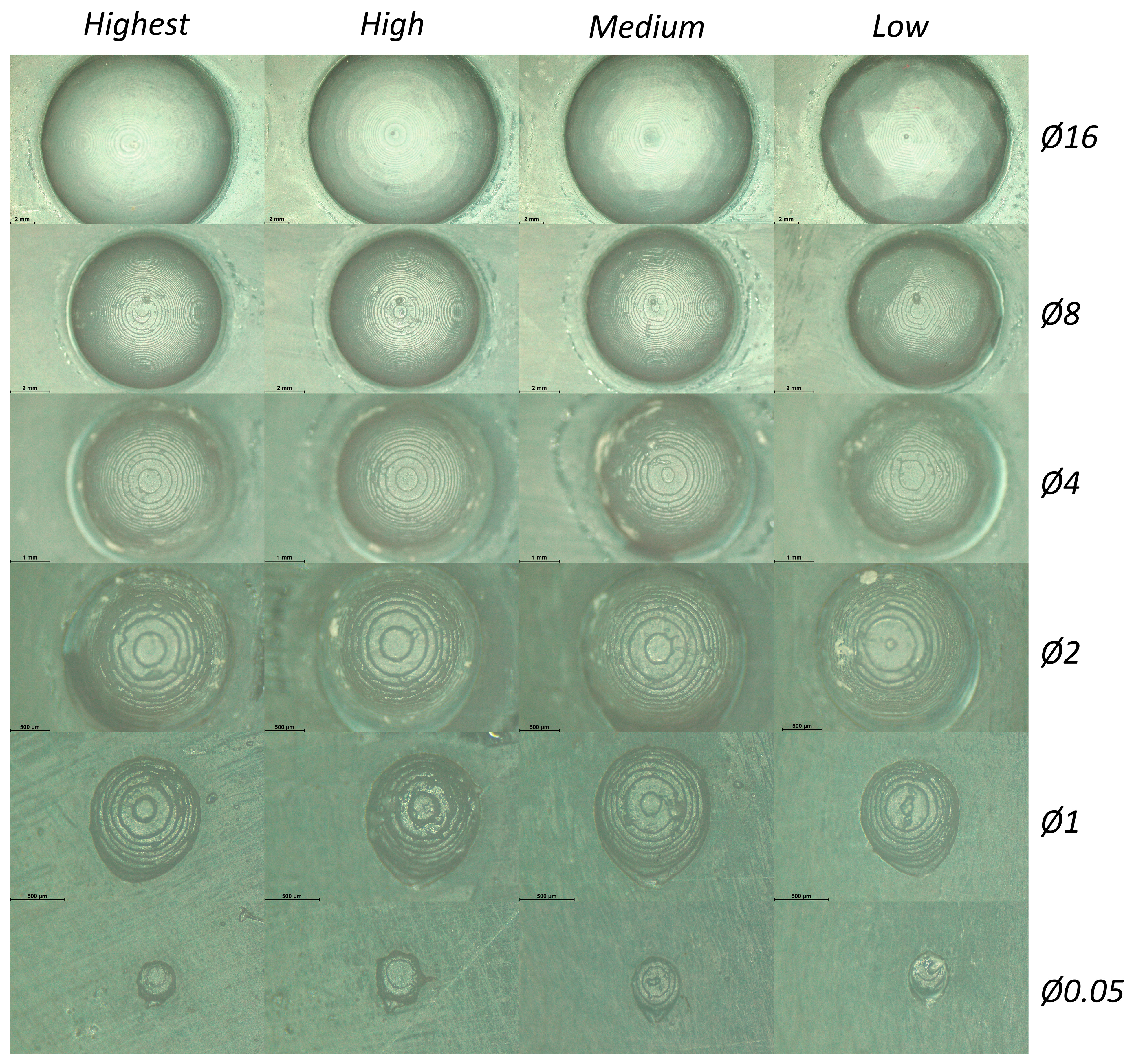
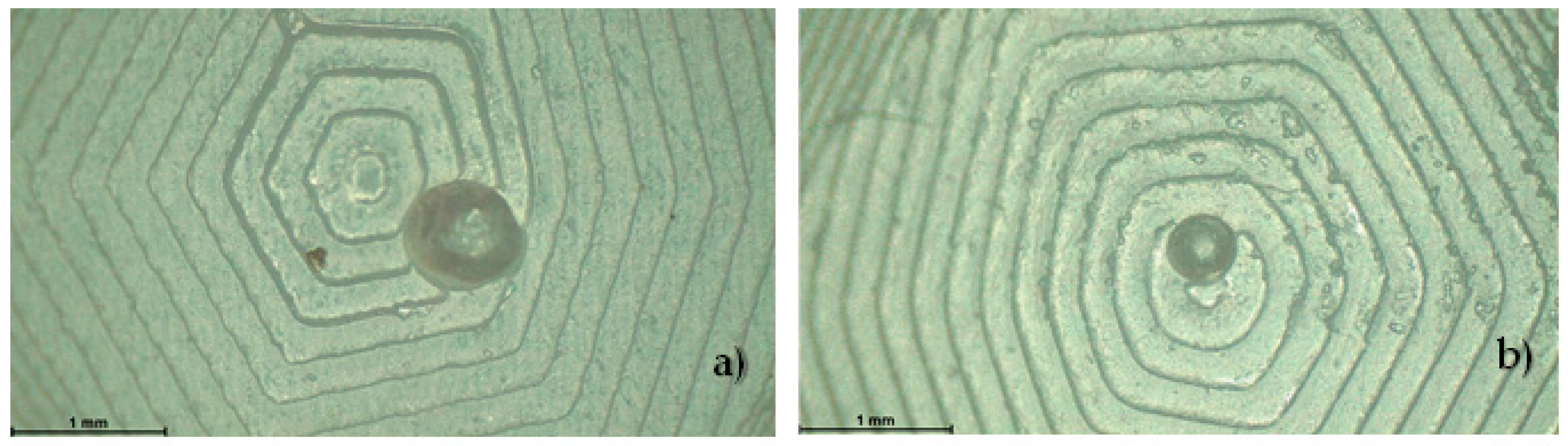
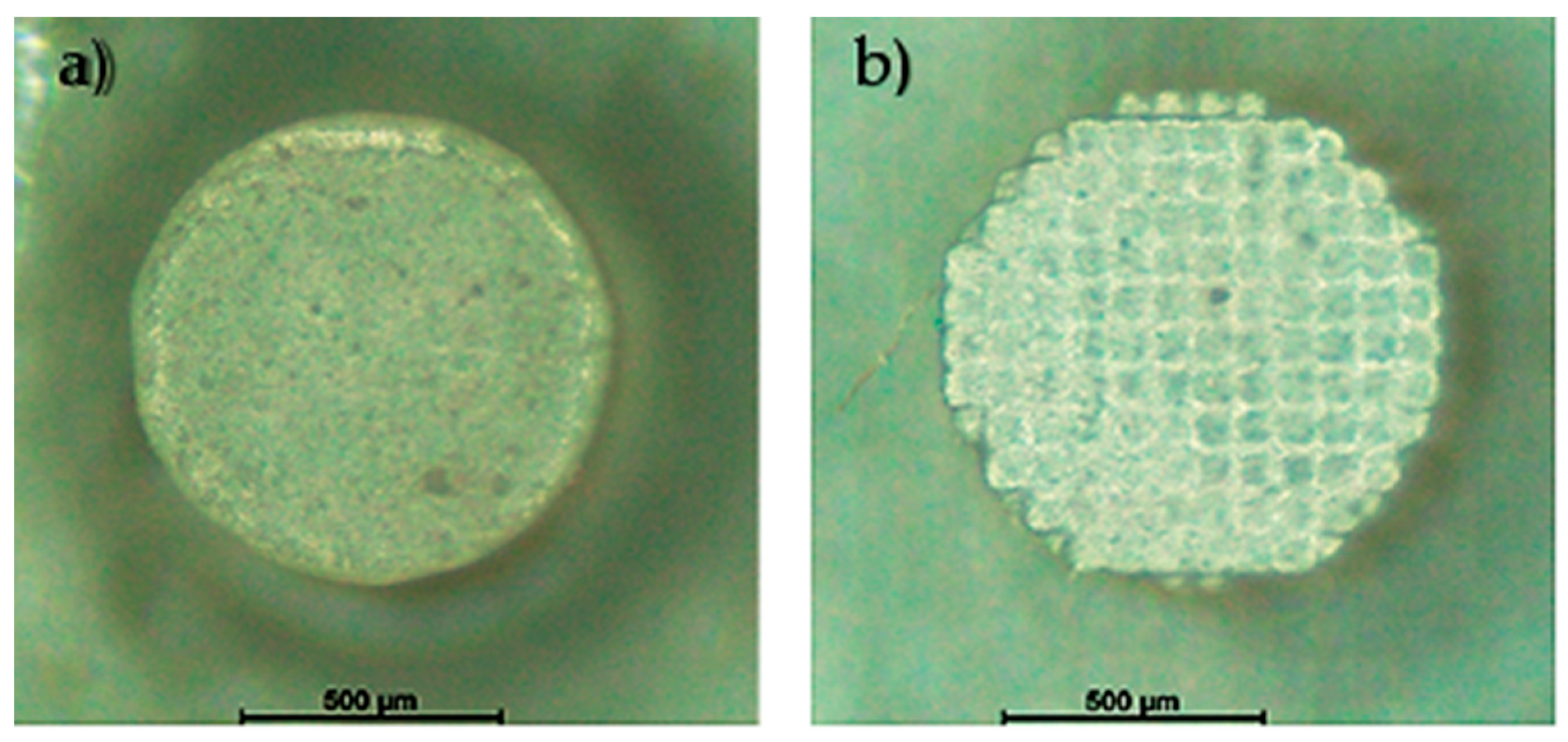
3.1. STL Performance Analysis

As has previously been mentioned, the increase in resolution during the export of a 3D model results in a longer file processing time and a higher computational cost. However, in the specific case of VPP manufacturing technology, a high surface quality is usually sought in the parts obtained, so the discretisation process is of great importance, as it will decisively affect the final quality of the part. If we analyse the amount of information stored in the files (Table 3), we can see that there is an almost linear relationship with the increase in size, so the processing can become more complicated as the resolution increases, this being understood as the size of the polygons that make up the mesh. For this reason, we will analyse how this resolution and the size of the figures affect the pieces obtained.
Figure 4 shows the geometries obtained, depending on the different resolutions and sizes, for LCD technology.
In the case of the lowest resolution, the polygons with which the geometry has been discretised can be seen, and as the resolution increases, the polygons into which the part is divided are smaller and therefore, less visible, until, in the case of the highest resolution, they are no longer visible to the naked eye, and the cylindrical layers that make up the part can be seen. In this way, the increase in resolution causes the upper portion of the part to go from being seen as irregular hexagons to concentric circles that are stacked to build the part.
On the other hand, when analysing the influence of the size of the hemispheres, it can be seen that, regardless of the resolution, as the size of the hemispheres decreases, the manufactured features have a similar visual appearance. In this way, in parts with a diameter of 4 mm, the discretisation is not as visible, but there are still irregular shapes that make up the part. However, from 2 mm diameter parts onwards, the triangles discretised by the STL file are no longer visible to the eye, and only circular layers are visible. Thus, this is the point at which the necessary limit of resolution is found.
In the case of DLP technology, the result is similar: in the larger hemispheres, the triangles that form the mesh are visible, while from 2 mm in diameter, they are no longer noticeable (Figure 5).
Therefore, it can be said that, in the case of the manufacture of parts with spherical characteristics with a diameter of 2 mm or less, the resolution of the mesh is not significant. However, for larger parts, a high resolution is required when meshing; otherwise, the polygons that make up the mesh will be visible. On the other hand, there are no significant differences between the two technologies; however, it can be seen that the higher XY resolution of LCD technology means that the smaller hemispheres are better defined. This is something that will have a decisive effect on the analysis of 2D deviations.
However, in both cases, defects associated with the reloading of the material can be seen, which is a negative effect that appears in these processes [34,38] and which can be seen in the upper area of the figures, mainly in the larger ones (Figure 6). It can therefore be deduced that this effect is independent of the resolution of the figure and the technology.

3.2. The 2D Deviation Analysis

As mentioned above, a study of the lateral deflections has been carried out from the analysis of the perimeter of the designed geometries. Once the manufactured specimens were analysed, the data obtained were processed.
When analysing the figures, the first thing that can be seen is a pixelated effect in the case of DLP technology, something that is characteristic of this technology [17] and which is not seen with LCD technology. This effect appears, independently of the geometry and resolution, as can be seen in Figure 7.
On the other hand, if the images are analysed as a whole, it can be seen that in the case of the LCD technology (Figure 8), regarding the positive and negative geometries, increasing the exposure time slightly improves the accuracy of the corners up to 8 s. If it is increased further, negative effects occur. In the case of DLP technology, similar behaviour occurs (Figure 9), so it follows that exposure times significantly affect figure accuracy. To study the effects more concretely, the perimeter of these figures will be analysed.
In order to study these effects, firstly, the main effects graph was obtained for each of the different geometries. This type of graph provides an overview of the influence, or lack thereof, of the factors on the measured variable, in this case, the perimeter (Figure 10). Analysis of the graph shows that the most significant factors are the direction of manufacture and the type of technology used. On the other hand, it is generally observed that the exposure time has practically no effect on the measured perimeter.
Taking into consideration the manufacturing direction factor, there is a clear trend showing that the manufacture of shafts is able to reproduce average values of the perimeter close to the design perimeter. On the other hand, the parts manufactured as hollows significantly exceed the design values, regardless of the exposure time applied and the manufacturing equipment used.
Likewise, it can be seen that the parts manufactured with LCD technology present mean experimental values of the perimeter closer to the design values, while those manufactured with DLP technology far exceed the values of the established model. It can also be seen that the average of the perimeter values obtained exceeds the theoretical design perimeter, without taking into account any of the aforementioned factors.
It can be seen that the mean value of the perimeter measured in all experiments is 24.2122 mm, while the theoretical value of the designed perimeter is 24 mm. The relative error between the two measurements is 0.884%.
It can be concluded that the experimental results of the average circumference obtained were above the design values, i.e., parts with larger dimensions have been manufactured, although the relative error between both values is very small.
These graphs provide some information about the main effects of the proposed factors on the selected measurements. However, in order to correctly establish the significant factors of an experiment, it is necessary to carry out an ANOVA test. With this analysis, the actual significant factors of a study are obtained. The common ANOVA test has a confidence level or interval of 95%, where α = 0.05. Table 4 shows the p-values obtained for each factor, with the aim of establishing those that are significant in this study.
It can be seen that the significant factors in the three geometries correspond to those listed above in the main effects plots. This shows that the values observed in the main effect plots are valid, in this particular case, to establish the significant factors affecting the response variable. This table shows that the exposure time in the different geometries is still not a significant factor in the study; on the other hand, as shown in the main effect plots, both the manufacturing direction and the machine used are significant factors in the process, and as a consequence, these factors influence the perimeter.
As in the main effects graphs and in the ANOVA tests carried out, the Pareto diagram (Figure 11) shows that the main significant factors in the study are the manufacturing direction and the technology used, as they exceed the critical value, indicated by the red dashed line. Furthermore, the interactions between the different factors are shown in this graph, and the interaction between exposure time and manufacturing direction is significant.
All the graphs and diagrams shown above represent the influence of each of the factors on the response variable; however, it is also important to consider the interaction between the different factors. Figure 12 shows the factor interaction graph.
Observing the graphs, it can be seen that in the interaction of the machine–direction factors, there are appreciable differences between the values. On the one hand, it can be seen that parts manufactured using DLP technology show higher average perimeter values than those manufactured with LCD technology. In addition, the difference between manufacturing a hollow and a shaft is easily visible, since it is the significant factor that has the greatest impact on the response variable, according to the data obtained.
Analysing the interaction between exposure time–machine, it can be seen that there are small variations in the data when the exposure time varies. However, analysing the variations in the technology used, there are notable differences between the elements manufactured with DLP and LCD technology, with those obtained with LCD being closer to the design specifications.
Finally, looking at the exposure time–direction interaction graph, there are also variations among the data. There is a tendency for the perimeter values between the shaft and hole to equalize as the exposure time increases. In the case of exposure time at level 1 (lower exposure), there are notable differences between the perimeter values for the shaft and hole; however, when the exposure time is at level 3 (higher exposure), these data tend to equalize, and there are practically no differences between the shaft and hole.
However, it has been determined that the exposure time is not a significant parameter in regards to the response variable, so it has been difficult to establish an optimal exposure time for each technology.
Going deeper into the research, the designed pieces have the shape of sockets, so their function could be the union between shaft and shaft; therefore, it would be important to take into account the situation in which the perimeter measurements are similar in both the shaft and the shaft. Observing the interaction graphs between variables, specifically the interaction between exposure time–direction, it can be seen that the minimum difference between the experimental values of the mean perimeter obtained for the axis and shaft occurs when the exposure time is the highest, i.e., level 3. This corresponds to an exposure time of 2.5 s, in the case of DLP technology, and 8 s, in the case of LCD technology. Therefore, these exposure times could be the optimum parameters of the study, since although the values are far from the theoretical value, they are similar for the shaft and gap.
This has also been analysed in a practical way, fitting the pieces obtained to observe their behaviour. It has been observed that practically all the pieces have fitted correctly. In the case of the parts obtained with shorter exposure times (level 1 and 2), for both technologies, the parts fitted easily, due to the looseness of the hollow-shaped parts and the smaller size of the shaft-shaped parts. However, it is of interest that these parts fit without clearance, so the parts obtained with the longest exposure time have fulfilled this requirement. The interaction graphs between factors show that the dispersion of values is low.
In short, examining all the data obtained, it can be said that with the realization of this study, optimal exposure times have been taken for each of the manufacturing equipment used. In the case of the DLP technology machine, the optimum exposure time is 2.5 s, while for the LCD technology, it is 8 s. This choice of exposure times was based on the design objective of these parts, i.e., the way they fit together. As mentioned above, the choice of shorter exposure times could have been valid because the parts fit together, but they fit loosely, and this is due to the difference in perimeters between the gap and the shaft of the same part. With the longer exposure time, therefore, the pieces fit correctly and without looseness, since the perimeters of the shaft and shaft are similar.

3.3. Pyramidal Speciments

Figure 13 shows the pyramid-shaped parts obtained with DLP technology and LCD technology, respectively. The first noteworthy aspect is that the only pyramid that exhibits all the design features is the one produced with DLP technology. The rest of the pyramids manufactured with LCD technology have only been able to build 15 steps out of the 16 designed, where the last step has a diameter of 200 µm. Moreover, it can be seen that the pyramids obtained with DLP technology seem to better represent the designed model.
The results obtained after the measurement process are shown in Table 5. Analysing the data, it is observed that the experimental values are generally about 20 µm away from the theoretical value. This means that there is a relative error of between 12% and 9% for the experimental values, with respect to the theoretical values. Although this error is not significantly large, the experimental results can be considered to be relatively far from the theoretical specifications.

4. Conclusions

VPP techniques are pivotal in advancing additive manufacturing (AM), with their research crucial for enhancing products across various sectors, particularly in medical and industrial fields. This study presents a geometrical analysis to examine the behaviour of LCD and DLP technologies. By analysing the geometrical aspects of both DLP and LCD methods, the impact of manufacturing parameters on the resulting features has been identified. Moreover, notable differences between these two technologies have been observed. The study also establishes optimal exposure times for each technology, based on the outcomes of various experiments. For LCD technology, the ideal exposure time is 8 s, which aligns with the default lamination program’s recommendation. In contrast, DLP technology requires an optimal exposure time of 2.5 s, which is slightly longer than the manufacturer’s suggestion of 2 s.
The precision of each technology along the XY axis has been assessed as well. Regarding the minimum feature size that can be fabricated, DLP technology consistently outperforms LCD technology, achieving feature sizes as small as 200 µm compared to LCD’s 500 µm. Additionally, DLP technology tends to produce features that are closer to the intended design values, especially in regards to smaller features, whereas LCD technology shows marginally better results in manufacturing larger parts. This enhanced precision in micro-feature fabrication using DLP may stem from the more intense light source used in DLP projectors compared to that used in LCD displays. However, LCD technology generally yields better visual quality in parts due to superior anti-aliasing systems that mitigate the staircase effect, which can distort the dimensions of features away from the design values. Geometrical analysis supports that features made with DLP are closer to design specifications compared to those made with LCD in micro-feature production. The study also explores the significance of the STL file resolution. It finds that for features smaller than 2 mm, the resolution of the STL file becomes less critical, whereas for larger features, the resolution of geometry discretization can significantly impact surface quality. A high-resolution STL file, when used for manufacturing larger parts, may significantly increase both processing time and file size. Finally, the accuracy of both technologies in the vertical axis was evaluated by measuring the heights of various pyramids, demonstrating that both technologies achieve similar accuracy in the Z-axis.

Author Contributions

Conceptualization, J.M.-J., J.M.V.-M. and M.B.; project administration, J.S. and J.M.V.-M.; experimental methodology, J.M.-J.; investigation, J.M.-J. and M.B.; data processing, J.M.-J. and M.B.; formal analysis, J.M.-J., J.M.V.-M. and M.B.; project review, J.S. and J.M.V.-M.; writing—original draft preparation, J.M.-J. and M.B.; writing—review and editing, J.S. and J.M.V.-M. All authors have read and agreed to the published version of the manuscript.

Funding

This research received no external funding.

Institutional Review Board Statement

Not applicable.

Informed Consent Statement

Not applicable.

Data Availability Statement

The original contributions presented in the study are included in the article, further inquiries can be directed to the corresponding authors.

Acknowledgments

This work has been developed under the support of the Mechanical Engineering and Industrial Design Department and the Vice-Rector’s Office for Scientific Policy of the University of Cadiz.

Conflicts of Interest

The authors declare no conflicts of interest.

References

  1. Rubben, T.; Revilla, R.I.; De Graeve, I. Influence of heat treatments on the corrosion mechanism of additive manufactured alsi10mg. Corros. Sci. 2019, 147, 406–415. [Google Scholar] [CrossRef]
  2. Gite, R.E.; Wakchaure, V.D. A review on process parameters, microstructure and mechanical properties of additively manufactured alsi10mg alloy. Mater. Today Proc. 2023, 72, 966–986. [Google Scholar] [CrossRef]
  3. Zhang, K.; Meng, O.; Qu, Z.; He, R. A review of defects in vat photopolymerization additive-manufactured ceramics: Characterization, control, and challenges. J. Eur. Ceram. Soc. 2023, 44, 1361–1384. [Google Scholar] [CrossRef]
  4. Ghungrad, S.; Haghighi, A. Three-dimensional spatial energy-quality map construction for optimal robot placement in multi-robot additive manufacturing. Robot. Comput. Integr. Manuf. 2024, 88, 102735. [Google Scholar] [CrossRef]
  5. Gibson, I.; Rosen, D.W.; Stucker, B.; Khorasani, M. Additive Manufacturing Technologies; Springer: Berlin/Heidelberg, Germany, 2021; Volume 17. [Google Scholar]
  6. Islam, A.; Mobarak, H.; Rimon, I.H.; Al Mahmud, Z.; Ghosh, J.; Ahmed, M.S.; Hossain, N. Additive manufacturing in polymer research: Advances, synthesis, and applications. Polym. Test. 2024, 132, 108364. [Google Scholar] [CrossRef]
  7. Gibson, I.; Rosen, D.W.; Stucker, B.; Khorasani, M. Development of additive manufacturing technology. In Additive Manufacturing Technologies; Springer: Berlin/Heidelberg, Germany, 2021; pp. 23–51. [Google Scholar]
  8. Gouttebroze, S.; Friis, J.; Hovig, E.W.; Boivie, K. Toward semantic standard and process ontology for additive manufacturing. In IOP Conference Series: Materials Science and Engineering; IOP Publishing: Bristol, UK, 2023; Volume 1281, p. 012014. [Google Scholar]
  9. Bandyopadhyay, A.; Bose, S. Additive Manufacturing; CRC Press: Boca Raton, FL, USA, 2019. [Google Scholar]
  10. Tofail, S.A.M.; Koumoulos, E.P.; Bandyopadhyay, A.; Bose, S.; O’Donoghue, L.; Charitidis, C. Additive manufacturing: Scientific and technological challenges, market uptake and opportunities. Mater. Today 2018, 21, 22–37. [Google Scholar] [CrossRef]
  11. Monzón, M.D.; Ortega, Z.; Martínez, A.; Ortega, F. Standardization in additive manufacturing: Activities carried out by international organizations and projects. Int. J. Adv. Manuf. Technol. 2015, 76, 1111–1121. [Google Scholar] [CrossRef]
  12. Tello, J.H.; Cervera, S.L.; Aymerich, J.T.; Ruiz, C.C.; Tardón, C.G.; Ayats, J.R.G.; Planas, S.M.; Calvet, J.V.; Puig, C.S.; Aragones, X.F. Diseño y Fabricación Inteligente; Recursos Educativos UOC Abiertos; Universitat Oberta de Catalunya: Cataluña, Spain, 2018. [Google Scholar]
  13. Hernández-Castellano, P.M.; Barcenilla, A.G.; Rivero, M.D.M.; Marrero-Alemán, M.D.; Hernandez, R.P.; García, L.A.S.; García, F.O. Tecnologías de Fabricación Aditiva; Servicio de Publicaciones y Difusión Científica de la Universidad de Las Palmas de Gran Canaria: Las Palmas de Gran Canaria, Spain, 2018. [Google Scholar]
  14. Zha, W.; Anand, S. Geometric approaches to input file modification for part quality improvement in additive manufacturing. J. Manuf. Process. 2015, 20, 465–477. [Google Scholar] [CrossRef]
  15. Paul, R.; Anand, S. A new steiner patch based file format for additive manufacturing processes. Comput. Aided Des. 2015, 63, 86–100. [Google Scholar] [CrossRef]
  16. Gibson, I.; Rosen, D.; Stucker, B. Vat photopolymerization processes. In Additive Manufacturing Technologies 3D Printing, Rapid Prototyping, and Direct Digital Manufacturing; Springer: New York, NY, USA, 2015; pp. 63–106. [Google Scholar]
  17. Pagac, M.; Hajnys, J.; Quoc-Phu, M.; Jancar, L.; Jansa, J.; Stefek, P.; Mesicek, J. A review of vat photopolymerization technology: Materials, applications, challenges, and future trends of 3d printing. Polymers 2021, 13, 598. [Google Scholar] [CrossRef]
  18. Miller, Z.; Stidham, B.; Fairbanks, T.; Maldonado, C. The use of stereolithography (sla) additive manufacturing in space-based instrumentation. In Proceedings of the IEEE Aerospace Conference, Big Sky, MT, USA, 4–11 March 2023; pp. 1–10. [Google Scholar]
  19. Zhang, F.; Zhu, L.; Li, Z.; Wang, S.; Shi, J.; Tang, W.; Li, N.; Yang, J. The recent development of vat photopolymerization: A review. Addit. Manuf. 2021, 48, 102423. [Google Scholar] [CrossRef]
  20. Tosto, C.; Pergolizzi, E.; Blanco, I.; Patti, A.; Holt, P.; Karmel, S.; Cicala, G. Epoxy based blends for additive manufacturing by liquid crystal display (lcd) printing: The effect of blending and dual curing on daylight curable resins. Polymers 2020, 12, 1594. [Google Scholar] [CrossRef] [PubMed]
  21. Bertsch, A.; Zissi, S.; Jezequel, J.Y.; Corbel, S.; Andre, J.C. Microstereophotolithography using a liquid crystal display as dynamic mask-generator. Microsyst. Technol. 1997, 3, 42–47. [Google Scholar] [CrossRef]
  22. Bove, A.; Calignano, F.; Galati, M.; Iuliano, L. Photopoly-merization of ceramic resins by stereolithography process: A review. Appl. Sci. 2022, 12, 3591. [Google Scholar] [CrossRef]
  23. Zhang, J.; Hu, Q.; Wang, S.; Tao, J.; Gou, M. Digital light processing based three-dimensional printing for medical applications. Int. J. Bioprinting 2020, 6, 242. [Google Scholar] [CrossRef] [PubMed]
  24. Tumbleston, J.R.; Shirvanyants, D.; Ermoshkin, N.; Janusziewicz, R.; Johnson, A.R.; Kelly, D.; Chen, K.; Pinschmidt, R.; Rolland, J.P.; Ermoshkin, A. Continuous liquid interface production of 3d objects. Science 2015, 347, 1349–1352. [Google Scholar] [CrossRef] [PubMed]
  25. Kuang, X.; Wu, J.; Chen, K.; Zhao, Z.; Ding, Z.; Hu, F.; Fang, D.; Qi, H.J. Grayscale digital light processing 3d printing for highly functionally graded materials. Sci. Adv. 2019, 5, 5790. [Google Scholar] [CrossRef] [PubMed]
  26. Kim, S.Y.; Shin, Y.S.; Jung, H.D.; Hwang, C.J.; Baik, H.S.; Cha, J.Y. Precision and trueness of dental models manufactured with different 3-dimensional printing techniques. Am. J. Orthod. Dentofac. Orthop. 2018, 153, 144–153. [Google Scholar] [CrossRef] [PubMed]
  27. Huang, J.; Qin, Q.; Wang, J. A review of stereolithography: Processes and systems. Processes 2020, 8, 1138. [Google Scholar] [CrossRef]
  28. Sun, C.; Fang, N.; Wu, D.M.; Zhang, X. Projection micro-stereolithography using digital micro-mirror dynamic mask. Sens. Actuators A Phys. 2005, 121, 113–120. [Google Scholar] [CrossRef]
  29. Gong, H.; Bickham, B.P.; Woolley, A.T.; Nordin, G.P. Custom 3d printer and resin for 18 µm× 20 µm microfluidic flow channels. Lab A Chip 2017, 17, 2899–2909. [Google Scholar] [CrossRef]
  30. Davoudinejad, A.; Ribo, M.M.; Pedersen, D.B.; Islam, A.; Tosello, G. Direct fabrication of bio-inspired gecko-like geometries with vat polymerization additive manufacturing method. J. Micromech. Microeng. 2018, 28, 085009. [Google Scholar] [CrossRef]
  31. Davoudinejad, A.; Cai, Y.; Pedersen, D.B.; Luo, X.; Tosello, G. Fabrication of micro-structured surfaces by additive manufacturing, with simulation of dynamic contact angle. Mater. Des. 2019, 176, 107839. [Google Scholar] [CrossRef]
  32. Jiang, C.P.; Meizinta, T. Development of lcd-based additive manufacturing system for biomedical application. In Proceedings of the International Conference on Artificial Intelligence and Robotics and the International Conference on Automation, Control and Robotics Engineering, Kitakyushu, Japan, 13–15 July 2016; pp. 1–6. [Google Scholar]
  33. Mohamed, G.A.; Kumar, H.; Wang, Z.; Martin, N.; Mills, B.; Kim, K. Rapid and inexpensive fabrication of multi-depth mi- crofluidic device using high-resolution lcd stereolithographic 3d printing. J. Manuf. Mater. Process. 2019, 3, 26. [Google Scholar]
  34. Pan, Y.; Zhou, C.; Chen, Y. A fast mask projection stereolithography process for fabricating digital models in minutes. J. Manuf. Sci. Eng. 2012, 134, 051011. [Google Scholar] [CrossRef]
  35. Dendukuri, D.; Pregibon, D.C.; Collins, J.; Hatton, T.A.; Doyle, P.S. Continuous-flow lithography for high-throughput microparticle synthesis. Nat. Mater. 2006, 5, 365–369. [Google Scholar] [CrossRef] [PubMed]
  36. Xu, Y.; Zhu, Y.; Sun, Y.; Jin, J.; Chen, Y. A vibration-assisted separation method for constrained-surface-based stereolithography. J. Manuf. Sci. Eng. 2021, 143, 051008. [Google Scholar] [CrossRef]
  37. Jin, J.; Yang, J.; Mao, H.; Chen, Y. A vibration-assisted method to reduce separation force for stereolithography. J. Manuf. Process. 2018, 34, 793–801. [Google Scholar] [CrossRef]
  38. Cheng, Y.L.; Lee, M.L. Development of dynamic masking rapid pro- totyping system for application in tissue engineering. Rapid Prototyp. J. 2009, 15, 29–41. [Google Scholar] [CrossRef]
  39. Choi, J.W.; Wicker, R.; Lee, S.H.; Choi, K.H.; Ha, C.S.; Chung, I. Fabrication of 3d biocompatible/biodegradable micro-scaffolds using dynamic mask projection microstereolithography. J. Mater. Process. Technol. 2009, 209, 5494–5503. [Google Scholar] [CrossRef]
  40. Pan, Y.; Chen, Y.; Yu, Z. Fast mask image projection-based micro- stereolithography process for complex geometry. J. Micro-Nano-Manuf. 2017, 5, 014501. [Google Scholar] [CrossRef]
  41. Gritsenko, D.; Yazdi, A.A.; Lin, Y.; Hovorka, V.; Pan, Y.; Xu, J. On characterization of separation force for resin replenishment enhance- ment in 3d printing. Addit. Manuf. 2017, 17, 151–156. [Google Scholar]
  42. Pan, Y.; He, H.; Xu, J.; Feinerman, A. Study of separation force in con- strained surface projection stereolithography. Rapid Prototyp. J. 2017, 23, 353–361. [Google Scholar] [CrossRef]
  43. Attaran, M. The rise of 3-d printing: The advantages of additive manufacturing over traditional manufacturing. Bus. Horiz. 2017, 60, 677–688. [Google Scholar] [CrossRef]
  44. Berman, B. 3-d printing: The new industrial revolution. Bus. Horiz. 2012, 55, 155–162. [Google Scholar] [CrossRef]
  45. Kim, J.H.; Lee, J.W.; Yun, W.S. Fabrication and tissue engineering application of a 3d ppf/def scaffold using blu-ray based 3d printing system. J. Mech. Sci. Technol. 2017, 31, 2581–2587. [Google Scholar] [CrossRef]
  46. Oh, Y.; Zhou, C.; Behdad, S. Production planning for mass customization in additive manufacturing: Build orientation determination, 2d packing and scheduling. In Proceedings of the International Design Engineering Technical Conferences and Computers and Information in Engineering Conference, Quebec City, QC, Canada, 26–29 August 2018. [Google Scholar]
Figure 1. Schematic diagram of the specimen, with hemispherical test patterns.
Applsci 14 03607 g001
Figure 2. Schematic diagram of the specimen, with positive and negative square test patterns.
Applsci 14 03607 g002
Figure 3. Schematic diagram of the pyramid specimen.
Applsci 14 03607 g003
Figure 4. Images of the hemispheres with different STL resolution and size, obtained with LCD technology.
Applsci 14 03607 g004
Figure 5. Images of the hemispheres with different STL resolution and size, obtained with DLP technology.
Applsci 14 03607 g005
Figure 6. Image of the recharge effects. (a) DLP technology in lowest resolution; (b) LCD technology in lowest resolution.
Applsci 14 03607 g006
Figure 7. Image of the pixelation effects. (a) LCD technology; (b) DLP technology.
Applsci 14 03607 g007
Figure 8. Image of the square test specimen obtained with LCD technology.
Applsci 14 03607 g008
Figure 9. Image of the square test specimen obtained with DLP technology.
Applsci 14 03607 g009
Figure 10. Graph of main effects on perimeter for square geometry.
Applsci 14 03607 g010
Figure 11. Pareto plot of standardized effects for square geometry.
Applsci 14 03607 g011
Figure 12. Factor interaction graph for square geometry.
Applsci 14 03607 g012
Figure 13. Pyramidal specimens.
Applsci 14 03607 g013
Table 1. Specifications of manufacturing machines.
SpecificationsPhoton SPhoton Ultra
Technology LCD DLP
Light source UV-LED Optical projector DLP
System resolutionFHD (2560 × 1440 px)HD (1280 × 720 px)
XY resolution 47 µm (0.047 mm)80 µm (0.080 mm)
Z-axis accuracy 0.00125 mm0.01 mm
Suggested layer thickness 0.01~0.2 mm0.01~0.15 mm
Exposure time6–9 s/capa1–3 s/capa
Manufacturing speed 20 mm/h60 mm/h
Power rating 50 W12 W
Manufacturing volume165 × 65 × 115 mm (HWL)165 × 102.4 × 57.6 mm (HWL)
System durability2000 h20,000 h
Wavelength405 nm405 nm
Table 2. Design of Experiment.
Experiment NumberExposure Time (s)GeometryTechnology
11 (1.5)Shaft (Positive)DLP
21 (1.5)Hole (Negative)DLP
32 (2)Shaft (Positive)DLP
42 (2)Hole (Negative)DLP
53 (2.5)Shaft (Positive)DLP
63 (2.5)Hole (Negative)DLP
71 (6)Shaft (Positive) LCD
81 (6)Hole (Negative) LCD
92 (7)Shaft (Positive) LCD
102 (7) Hole (Negative) LCD
113 (8)Shaft (Positive) LCD
123 (8)Hole (Negative) LCD
Table 3. STL file size for a sphere with different radiuses.
STL File Size (kB)
ResolutionElements by Radius of CurvatureElements by EdgeR = 10 mmR = 100 mmR = 1000 mm
Highest108949509760
High85504974909
Medium53302972850
Low23181751580
Table 4. ANOVA results.
PatternFactorp-ValueH0Significance
SquareExposure time (s)0.347AcceptedNo
Geometry0.000RejectedYes
Technology0.000RejectedYes
Table 5. Experimental results for the height of pyramidal specimens.
Manufacturing Technology
LCDDLP
GeometryAverage (μm)Standard Deviation (μm)Average (μm)Standard Deviation (μm)
Cylinder180717610
Disclaimer/Publisher’s Note: The statements, opinions and data contained in all publications are solely those of the individual author(s) and contributor(s) and not of MDPI and/or the editor(s). MDPI and/or the editor(s) disclaim responsibility for any injury to people or property resulting from any ideas, methods, instructions or products referred to in the content.

