1. Introduction
Graphene is an intrinsic zero-gap semiconductor, which can be chemically or structurally modified to satisfy specific needs of nanoelectronics and optoelectronics [
1–
5]. For instance, graphene nanoribbons (GNRs) result from a radical alteration of the graphene structure, where the reduction in dimensionality leads to a quasi-one-dimensional (1D) nanowire well suited for assembly into complex networks and nanocircuits with high-density functional units [
6–
10]. Compared to other options to build 1D carbon-based systems, such as carbon nanotubes, the planar nature of GNRs makes them particularly appealing, owing to the relative ease of their assembly into intricate geometries [
11–
13]. Theory predicts a broad set of singular properties [
14–
16], and advances in GNR fabrication have evolved at a fast pace. For instance, it is now feasible to grow narrow and pristine systems through pre-programmed and large-scale synthesis techniques [
11,
17–
21]. Even though the precise, controlled and scalable fabrication of carbon nanostructures with complex geometries remains a challenge from the experimental point of view, the developing bottom-up synthesis approaches of specific structures provide strong support to the eventual realization of this goal. Furthermore, depending on the details of their atomic structures, such as their widths and edge morphologies, GNRs’ physical properties, including their electronic, transport, magnetic and thermal behaviors, can be fine-tuned for a desired response to external stimuli [
14–
16,
22].
Monohydrogenated zigzag-edged nanoribbons (zGNRs) possess nontrivial spin distributions, due to the high charge density instability at their edges in a non-polarized (paramagnetic (PM)) spin distribution. Instead of undergoing geometric (e.g., Peierls) distortions or electrical polarization processes, zGNRs mitigate this instability by adopting a ferromagnetic spin ordering along each edge [
14,
16]. The ground state corresponds to an anti-ferromagnetic (AFM) edge-to-edge spin alignment [
16], where the two A and B graphene sub-lattices display a net spin-up and -down population, respectively. While direct experimental evidence for the existence of these stable spin states at room temperature is still lacking [
23,
24], published experimental data suggest the existence of such edge states, as scanning tunneling spectroscopy (STS) patterns measured in edged graphene samples can only be explained theoretically by considering spin polarization at the system edges [
19,
25]. It follows that the conduction and valence bands in zGNRs are quasi-one-dimensional and correspond to localized states extending over the edges of the system. These states are essential to the physics of zGNRs, since they govern low-bias conduction processes. By definition, such edge Bloch states do not mix with states delocalized across the zGNR width. This attractive property turns out to become a potential curse for building up complex zGNR-based networks, since low-bias electrons will always flow along a given set of connected edges belonging to the same sub-lattice, effectively not penetrating deep into the network and, thereby, reducing drastically the number of useful operations that can be programmed into the network connections.
In this paper, we describe the concept of a zGNR-based heterospin junction. While GNR hetero-junctions based on the assembly of different geometries (involving both aGNRs and zGNRs) [
26] or on the connection of multiple terminals [
27] have been considered before, here, we study a type of heterojunction made solely of zGNRs prepared in different spin distributions. The concept of a purely zGNR-based heterospin junction has been visited before, where it was shown that a mismatching mechanism, originating at the electrodes with opposite FM distributions, is responsible for the onset of magnetoresistance in such junctions [
22]. Instead, we here focus on a different junction with AFM electrodes and show that it possesses the property of allowing edge states to hop from one edge to the other, generating a net inter-edge current. First, pristine AFM zGNRs are shown to present interesting properties, like half-metallicity upon an applied electric field [
14]. Second, our results highlight the emergence of a new feature, namely the edge-to-edge transmission, underscoring the importance of understanding the behavior of basic building blocks, like GNRs, in more complex systems. This aspect is of fundamental importance in the practical use of GNRs in complex nanocircuits, since low bias transport in these systems usually occurs along the edges of the structure. We adopt the framework of quantum transport, where the basis of stationary states is replaced by the concept of scattering in an open-system with boundary conditions set at the electron reservoirs far from the interface region. We show that a proper choice of boundary conditions, compatible with those of bulk zGNR electrodes, yields the coveted possibility of directing edge states from one edge to the other without any structural modifications. Despite its simplicity, this problem can serve as a basic model to understand electronic flow in graphitic systems with complex edge arrangements. The heterojunction is thoroughly analyzed using a combination of methods, including the quantum transport, S-matrix and eigenchannel decomposition approaches.
2. Systems and Methods
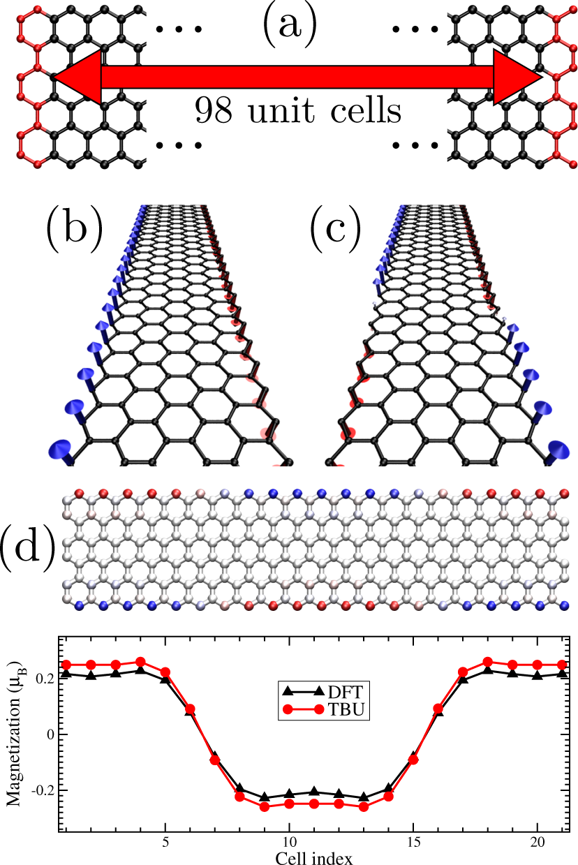
The systems under scrutiny consist of AFM heterospin junctions made up of a single defect-free zGNR (
Figure 1a). To design such junctions, we connect two semi-infinite pristine zGNRs prepared in their AFM ground states, with the essential difference between them being that the degenerate states are chosen to correspond to an AFM and inverted AFM
distributions far from the connecting region. The spin distribution is then obtained self-consistently in the rest of the system. This constraint, applied far from the interface, leads to the development of an effective
heterospin junction. Examples of an AFM-homojunction and the corresponding heterojunction are depicted in
Figure 1b,c. We will consider a series of heterojunctions composed of different zGNR-
n, where the number
n of zigzag strips across the ribbon width takes on a set of values ranging from 4 to 40.
The electronic properties are computed using a self-consistent
π-orbital tight-binding description (TBU) that includes interactions up to third nearest-neighbors and a Hubbard term to account for spin-spin interactions, as detailed in [
8]). The numerical values for the tight-binding hopping integrals are
γ1 = 3
.2 eV,
γ2 = 0 and
γ3 = 0
.3 eV for first-, second- and third-neighbor sites (overlap integrals are taken as zero). The first-neighbor hopping integral is reduced by a ∆
γ1 = 0
.2 eV correction on the edge atoms to account for the different chemical environment at those sites [
28]. The Hubbard on-site parameter is given by
U = 2
.944 eV, as determined by fitting with density functional theory calculations [
8]. The converged Hamiltonian matrices are recast into an open-system setup appropriate for a Landauer–Green’s function framework to compute the quantum conductance in extended systems [
29]. Green’s function (GF) for the central scattering region is obtained by the application of a set of efficient recursive algorithms recently proposed [
30,
31]. To validate results obtained with TBU, spin-polarized density functional theory (DFT) calculations were performed using the VASP package [
32,
33] within the generalized gradient approximation (GGA) using the Perdew–Burke–Ernzerhof (PBE) exchange-correlation functional [
34]. In DFT, we performed non-collinear spin calculations to make it possible to impose proper boundary conditions corresponding to the heterospin junction. Comparison with TBU was performed for the system described by a supercell composed of 18 unit cells of a zGNR-6 (
Figure 1d). We constrained the spin polarization on the edges for the first three and the other three intermediate unit cells to an AFM and an
configuration, respectively. For DFT, only the direction of magnetic moments was constrained while their magnitude was allowed to relax. While imposing the spin constraints in those cells, the spin distribution on the other cells was unconstrained and obtained in a self-consistent manner. The resulting graph in
Figure 1d shows atomically-resolved magnetic moments along one edge for both DFT and TBU and indicates that all of the features of the spin distribution are in quantitative agreement. Note that, for the TBU-based transport calculations, we performed a self-consistent calculation to obtain the converged Hamiltonians using a larger number of unit cells in the central region while constraining the spin to the bulk AFM distribution for the cells corresponding to the leads, to ensure proper convergence with the system size.
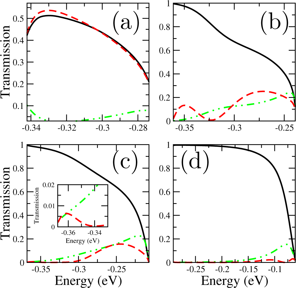
3. Electronic Transmission
To compute the electronic transport in the heterojunctions, we used the TBU approach to simulate the central channel region made up of 98 zGNR-
n unit cells attached to two zGNR-
n terminals (
n = 4, 6, 8, 10). The leads are constrained to maintain the bulk AFM distributions, and the spin configuration in the right terminal is inverted relative to the left one for the case of the heterojunction. In practice, preparing the electrodes in such a magnetic state will require the use of appropriate contacts with a controllable spin state [
35]. In
Figure 2, we plot the conductance for the occupied states (
E <
EF = 0, where
EF denotes the Fermi energy) for the spin-up states as a function of energy for both the heterojunction (solid black lines) and the perfect system (dashed red lines) for the zGNR-
n junctions. Because the system remains in an AFM overall distribution, the plot is identical for spin-down and is symmetrical relative to
E =
EF, within the TBU approach (note that while we consider third neighbor interactions, the second neighbor parameter is zero, preserving the electron-hole symmetry [
28]).
We examine the conductance spectra for negative energies in the pristine system and identify two main regions: (I) the energy range characterized by a single conducting channel; and (II) the region for the conductance plateau corresponding to two channels. These regions are indicated by dashed and full double arrows, respectively, in the left-hand side plots in
Figure 2. Among the two spin-polarized channels in Region (II), one is strongly localized along one edge [
14,
16]. The main result from the conductance plot for the heterojunctions in this energy region is that the edge state does have a finite probability to hop from one edge to the opposite one. To better understand the details of the transmission and elucidate the transport process, we performed an eigenchannel analysis, where the electronic transport theory is formulated into the equivalent scattering-matrix (S-matrix) method [
36,
37]. Here, we express the S-matrix on the basis of the Bloch states of the isolated electrodes, as a natural choice to assess the possibility of transmitting edge states from one edge to the opposite one. It follows from the definitions given above that the S-matrix is a 2
× 2 and a 4
× 4 matrix in Regions (I) and (II), respectively. For the heterojunction, we observe that the single channel in (I) transmits with a 100% probability, while electronic states impinging at energies located in Region (II) are strongly affected by electronic scattering. We observe that the conductance for energies in the right sector of Region (II) for the heterojunctions has a much lower value compared with the pristine system. This is a quantum mechanical effect that can lead to the construction of logic devices through the turning on and off of the electronic current, as in cross-bar GNRs, where the quantum phase provides a mechanism to control the out of plane electronic currents [
38]. In addition, the feature-rich transmission curve has a significant dependence on the system width. For example, the conductance for the zGNR-4 system in (II) shows a local maximum on the left-hand side of the interval, while the zGNR-8 and -10 systems present a peak of conductance on the right-hand side of (II). Interestingly, the zGNR-6 has an intermediate behavior with two clearly distinguishable peaks. We will now analyze further the mechanisms governing the physical processes responsible for the transmission across the interface.
4. Visualizing Electron Flow across the Interface
To visualize the electron flow across the interface, we computed the local current corresponding to a number of specific energies, as indicated in
Figure 2. The local current is computed using the current density operator, expressed in the Green’s function framework and projected on the atomic basis [
30,
39]:
where
Iij is the current between any two atomic sites,
i and
j,
is the hopping between these sites and
G< is the lesser GF. Neglecting electronic correlations, the retarded GF (
GR) can be used to obtain
G< by [
30]:
where the sum runs over all the terminals, Σ
l is the
l-th terminal self-energy and
fl is the corresponding Fermi distribution that describes the filling of the terminal states up to the chemical potential
μl. Here, we consider a Heaviside-like distribution, in the zero temperature limit.
The real space visualization is obtained by representing the local current data as:
where 〈
i|I|j〉 =
Iij and
with
r being the distance from the point (
x, y) to the position of site
i and
aCC is the bond length in graphene. As
Iij =
−Iji (see
Equation (1)), we select only the positive values of
Iij by setting
αij = 1 (0) when
Iij ≥ 0 (
Iij < 0). Even though the equations for local current are only formally correct for full non-equilibrium, self-consistent calculations, they remain applicable for a qualitative analysis at low-bias potential. While the study of non-equilibrium transport, including inelastic effects, is out of the scope of this work, such a methodology can be expanded to include accurately the effect of finite bias [
40,
41]. In addition, it is expected that the application of a small bias will not disrupt the spin ordering, as is the case with GNRs conducting high currents [
42,
43]. For comparison purposes, we also plot the current flow distribution at the same energy for the corresponding homojunction. The plots for the homojunctions confirm that the electrons with energy lying in Region (II) proceed quasi-exclusively along the edges.
We now discuss the zGNR-6-based junction in more detail: we note that the current density along the edge is significantly more intense for energies farther away from the Fermi energy. As we will show now, this result is due to the symmetry properties of the eigenstates in the pristine lead. To clarify this point, we examine the local charge density for the highest occupied band at different values of the k vector for the zGNR-6 calculated with the TBU approach (
Figure 3). The selected k values marked from 1 to 3 (Region (I)) correspond to states spatially delocalized over the entire ribbon width. Conversely, the states become more and more localized at the edge as we move from Point 4 to Point 11 (Point 6 is located at the top of the band, and Point 11 marks the edge of the Brillouin zone), in Region (II). Clearly, the electronic transport for energies in Region (II) is supported by two states with distinct spatial localization: one state is localized on the ribbon’s edge (between k Points 6 and 11), while the other is delocalized over the width of the system. Note also that the relative difference in the degree of localization is higher for energies on the left-hand side of the two-channel plateau (energies close to that from Point 11) than for energies on the right (close to the energy corresponding to Point 6). Performing this analysis on the heterojunction, we observe that the delocalized states have a large probability to be transmitted across the interface, given the significant overlap between such a state on one side of the interface and the corresponding state on the other side. By the same token, it would seem that the more localized state should have a much smaller transmission probability to the equivalent states on the other side of the interface. However, care must be taken in making such a claim, since these states are no longer stationary states of the interface system, and we expect that cross-state transmission should take place. Such an analysis is best performed within the S-matrix formalism, since it can highlight the important interference effects across the interface, as discussed below.
The local current plot in
Figure 2a establishes that the left conductance peak in zGNR-4 corresponds mostly to the transfer of the current from one edge to the other, as one of the Bloch states for this energy is highly localized along the edge and benefits from the narrow width of the system to the tunnel. Now, analyzing the plot for the corresponding peak in zGNR-6 (
Figure 2b), the edge-to-edge contribution for the current is still present, but with a smaller relative contribution to the current over the ribbon’s valley. This is mostly due to the presence of the other delocalized Bloch state at the same energy. The wider geometry also weakens the coupling between opposite edges, compared to narrower ribbons. Note that the peak on the left is suppressed for the zGNR-8 and wider systems as the overlap between the Bloch states localized on opposite edges is significantly reduced (see the left panel of
Figure 2). Moving to the peaks in the right-hand side of Region (II), whose corresponding edge Bloch state is slightly less edge-localized than those from the left part of Region (II), we observe that they still produce a dominant inter-edge current in zGNR-6 (
Figure 2c), but the relative weight of this contribution in comparison to the valley current decreases as we increase the width of the ribbon (see
Figure 2d,e).
5. Eigenchannel Analysis: Scattering of the Electrode’s Bloch States
A more detailed understanding of the scattering phenomena is obtained by identifying the transmission contribution from the individual states from the leads (
Figure 4). Here, we focus on the energy Range (II) corresponding to the discussion on
Figure 2. This range is highlighted by the shaded area in the plot from the left-hand side of
Figure 3. There are two electronic states for each energy value in this range: one for a
k-vector smaller than
k6 (with
k6 being the
k-vector of Point 6 in
Figure 3) and another one for a
k-vector larger than
k6. To simplify the subsequent discussion, we will refer to the first electronic level (
k <
k6, which is less localized) as the valley state, or simply as channels
and
in the left and right terminals, respectively. The second level (
k >
k6, which is localized along the edges) will be referred to as the edge state, or simply as channels
and
for the left and right electrodes. First, for zGNR-4 (the narrowest system studied here; see
Figure 4a), we observe that the transport is balanced between valley-to-valley (
; black full line) and edge-to-edge (
; red dashed line) tunneling, with a minor cross-channel contribution (
and
; green dashed dotted line). The inter-edge transmission is favored by the narrow width, so that the electrons belonging to
can more effectively transmit to
and to a lesser extent to
. Moving to wider systems, we observe that the edge-to-edge contribution to the current (red dashed lines in
Figure 4) weakens in comparison to the valley current (black full lines in
Figure 4) as the ribbon width increases. This effect is accompanied by an enhanced transmission of the
channel into the right valley eigenstate
. Comparing these results with those of the zGNR-6 and -8 systems (see
Figure 4b,c), we now understand how the contribution of the (edge-to-valley) cross-channel tunneling gradually becomes more important than the direct inter-edge transmission as the ribbon gets wider.
To further understand the effect of GNR width on transport behavior, we consider the wider ribbon zGNR-40 (
Figure 4d) and observe again that the
channel transmits mostly to
(
∼ 80% at
E =
−0
.1
eV, for instance). However, the mechanism is different for the edge channel, as the inter-edge tunneling
is suppressed relative to the interchannel
transmission. Clearly, the widest system does not allow sufficient overlap between the two
and
eigenstates of the leads, so that this reduced inter-edge coupling prevents a strong tunneling from taking place between the opposite edges of the structure.
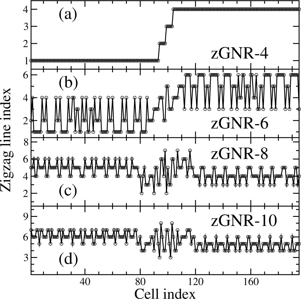
It is not trivial to determine the crossover between edge and valley transport regimes, since valley currents spread over broad spatial ranges, being shared by a number of zigzag strips along the system width. In contrast, edge currents are limited to a narrow portion of the ribbon. In order to gain further insight on this point, we consider spin-up states and plot the atomic position of the largest inter-site current (as a function of the index of the zigzag strip along the ribbon width) for each zGNR unit cell along the junction for the zGNR-4, −6, −8 and −10 cases in
Figure 5. Here, we considered the energy values denoted by (a), (c), (d) and (e) in the left side of
Figure 2. Note that the largest current is on the edge with a net spin-up polarization for the zGNR-4 case, except for the interface cells. Even though this is not strictly true for the zGNR-6 case, the zigzag strip presenting the largest current is usually the edge one. In other words, despite the fact that the valley states transmit more than the edge ones, the valley current is shared by a number of zigzag strips, so that most current flows along the edges of the system. The largest current is then moved to the valley region for zGNR-8 and wider systems. This shows that the heterospin system has a limiting behavior when moving from the zGNR-6 to the zGNR-8 system.
Furthermore, as pointed out before, the
transmission for the zGNR-6 system behaves differently compared to wider systems, since it presents two prominent peaks centered around
−0
.35 eV and
−0
.27 eV in the energy Range (II), resulting in a dip around
−0
.32 eV. Analyzing this result carefully, we find that such a double-peak feature is also present in the zGNR-8. However, in this case, the peak at lower energy is significantly less intense than the one at a slightly larger energy, as shown in the insert of
Figure 4c. The emergence of such a feature is directly related to the nontrivial dependence of the
overlap as a function of energy (data not shown).
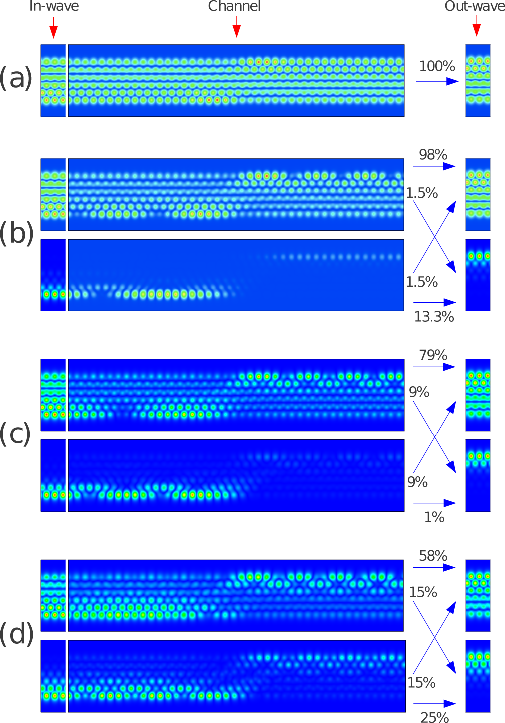
Finally, we provide a state-resolved visualization of how individual Bloch states of the left lead scatter into right lead states using transfer matrix techniques along with the corresponding coefficients of the S-matrix at specific energy values [
44,
45]. This analysis allows for plotting the scattering wave functions, as illustrated in
Figure 6 for the zGNR-6 system. The calculation is performed by considering incoming Bloch states deep from the electrode and visualizing how the scattered states tunnel into the Bloch states of the opposing electrode. For an electron in the energy range of Region (I), the interface is quasi-completely transparent (see
Figure 6a). We computed the eigenchannels for the energies in Region (II) for the left (
Figure 6b) and right peaks (
Figure 6d) and for the dip between them (
Figure 6c). As indicated by the data in
Figure 4b and in
Figure 6b–d, the
transmission (equal to 98%, 79% and 58%, respectively) experiences a monotonic decrease in Region (II) as we move to energies closer to
EF. Note that, even though this transmission is the largest one, the corresponding current is spread over the ribbon width, so that most current flows along the edge. This trend is opposite of the cross-channel tunneling (indicated by crossing arrows plotted in
Figure 6b–d). The less trivial behavior for the inter-edge tunneling is manifest in the
transmission (from 13.3% in the left conductance peak to 25% in the right one, passing by 1% in the midway dip) given the smaller overlap between
and
across the interface for the energy in the dip, in spite of their localization degree being intermediate between the corresponding states in the left and right peak energies.


