
High-Resolution Digital-to-Time Converter Implemented in an FPGA Chip


Key Laboratory of Electronic Equipment Structure Design, Ministry of Education, School of Electro-Mechanical Engineering, Xidian University, Xi’an 710071, China
*
Author to whom correspondence should be addressed.
Appl. Sci. 2017, 7(1), 52; https://doi.org/10.3390/app7010052
Submission received: 9 November 2016
/
Revised: 24 December 2016
/
Accepted: 27 December 2016
/
Published: 4 January 2017
Abstract
:This paper presents the design and implementation of a new digital-to-time converter (DTC). The obtained resolution is 1.02 ps, and the dynamic range is about 590 ns. The experimental results indicate that the measured differential nonlinearity (DNL) and integral nonlinearity (INL) are −0.17~+0.13 LSB and −0.35~+0.62 LSB, respectively. This DTC builds coarse and fine Vernier delay lines constructed by programmable delay lines (PDLs) to ensure high performance delay. Benefited by the close-loop feedback mechanism of the PDLs’ control module, the presented DTC has excellent voltage and temperature stability. What is more, the proposed DTC can be implemented in a single field programmable gate array (FPGA) chip.
1. Introduction
A digital-to-time converter (DTC) is similar to a digital-to-analog converter (DAC), except that DTC converts digital values to time interval signals. DTCs are widely used in atomic frequency standards, high-precision positioning [1,2], time-correlated single-photon counting instruments (TCSPC), and measurement instruments [3,4,5,6] such as the very large scale integration (VLSI) functional tester [7].
The counting method is a widely used DTC method, which is realized by counting periods of a reference clock. The counting method is simple in implementation and large in dynamic range. However, its resolution is limited to several nanoseconds, which is determined by the frequency of the reference clock. Taking advantage of the technique of the Application Specific Integrated Circuit (ASIC), DTCs implemented in ASIC devices (ASIC-based DTCs) have been proposed [1,2,3,4,7]. The best resolution of the ASIC-based DTC is better than 1 ps [3], which is realized by combining the ASIC technique and the capacitor charging principle. However, these DTCs are sensitive to variations in temperature and voltage owing to the use of analog devices. Moreover, DTCs implemented in ASIC devices is high in cost and long in time to market.
With the development of commercial integrated circuits, DTCs implemented in FPGA (field programmable gate array) devices (FPGA-based DTCs) have attracted an increasing amount of research interest in recent years. Compared with ASIC-based DTCs, FPGA-based DTCs have the advantage of a low cost and a short time to market. Many DTCs implemented in the FPGA are realized by phase shifting [6,8,9], and the obtained resolution is about 8 ps. FPGA-based DTCs are mostly based on a Vernier delay line, a tapped delay line [10], and a Vernier ring oscillator [5]. A DTC with a resolution of 11 ps was implemented in a Xilinx Kintex-7 FPGA device based on a tapped delay line [10]. A DTC based on a Vernier ring oscillator and the Altera Stratix-III FPGA device was proposed [5], whose theoretical resolution was 1.58 ps.
DTCs with high resolution are mainly implemented in ASIC devices, which have the advantages of fully customized circuits and reasonably precise control of the internal propagation delay. However, it is difficult for FPGA-based DTCs to obtain high resolutions due to the additional delay introduced by the unpredictability of the routing strategy. Therefore, FPGA-based DTCs with a 1 ps resolution are very valuable for practical applications, but also very challenging for research.
In this paper, a novel realization of a DTC based on an FPGA device is proposed and tested. The obtained resolution is 1.02 ps, and the dynamic range is 590 ns. The proposed DTC benefits much from the coarse and fine Vernier delay line constructed by PDLs, which ensures a high performance delay. Meantime, the control module of PDL (programmable delay line) adopts a programmable close-loop feedback mechanism to adjust the tap delay of the delay lines, which improves the nonlinearity and stability of the DTC. Compared with the normal DTCs implemented in FPGA/ASIC devices, the proposed DTC achieves a higher resolution and improved nonlinearity and stability.
2. Principle of the Proposed DTC
2.1. Principle of the Vernier Delay Line
The Vernier delay line is widely used in time-to-digital converters (TDCs) [11]. The schematic of a TDC based on a Vernier delay line is shown in Figure 1. In the figure, time interval signals (Start and Stop) are delayed by two delay lines, respectively. The Start signal is delayed by a delay line with a cell delay of τ1, and the Stop signal is delayed by another delay line with a cell delay of τ2 (τ1 < τ2). When edge coincidence is detected, the measurement result can be calculated from Equations (1) and (2).
The principle of the Vernier delay line can also be applied to DTCs, which generate time interval signal (Start and Stop). The schematic of a DTC based on Vernier delay line is shown in Figure 2. Delay Line A and Delay Line B are adopted, which are with a cell delay of τA and τB. M is loaded into the counters as an input number, which is calculated according to the time interval needed. The output of the M-th delay tap in Delay Line A is the Start signal and the output of the N-th delay element in Delay Line B is the Stop signal. Thus, the generated time interval can be calculated from Equation (3).
2.2. Vernier Delay Line Realized by PDL
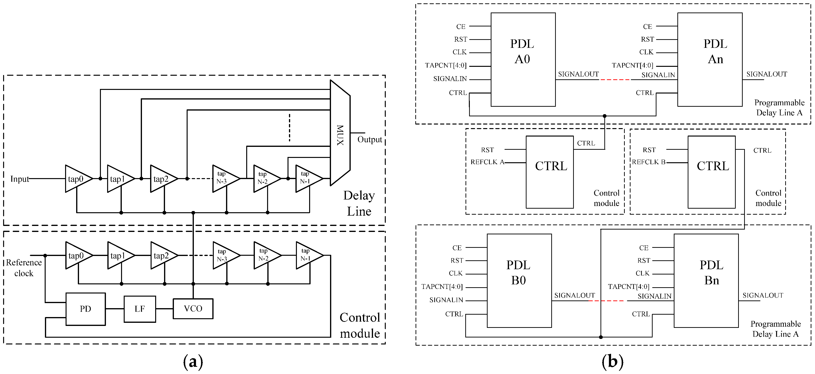
Herein, we use the programmable delay line (PDL) to realize the Vernier delay line. Figure 3a shows the schematic diagram of a PDL, which is a fully controllable, voltage-controlled, wrap-around delay line with a calibrated tap resolution. The control module is used to quantize a period of the reference clock and to ensure the time delay of the delay taps. If there are N taps in the delay line, the time delay of a single tap can be obtained from Equation (4). A control module can calibrate all the PDL modules within its clock region.
The delay taps in the delay line are voltage-controlled delay taps. In the control module, a phase detector (PD) is used to compare the output phase of the delay line with the reference clock. If the phase difference is not equal to half a period of the reference clock, the output of the phase detector changes the control voltage of the voltage-controlled oscillator (VCO), and the time delay of delay taps until the phase difference becomes coincident. The close-loop feedback mechanism reduces the influence from the voltage and temperature variations on the delay line. If variations of the voltage and the temperature lead to changes in the time delay of delay taps, a phase difference will be detected, and the close-loop structure will compensate the changes.
The time delay of delay taps in a PDL is determined by the frequency of the reference clock. For an N-tap delay line, the time delay of a tap is τA when the frequency of the reference clock is fA, and the time delay of a tap is τB when the frequency of the reference clock is fB. Therefore, the resolution of a Vernier delay line built by PDLs can be calculated from Equation (5). The schematic diagram of a Vernier delay line built by PDLs is shown in Figure 3b. The delay of a Vernier delay line built by PDLs can be programmed in two ways. First, the tap delay of PDLs can be programmed by changing the frequency of REFCLK A and REFCLK B. Second, the number of working delay taps can be specified by TAPCNT and the bit width, which is 5-bit (0~31). For the programmability, we call the delay line the programmable delay line.
2.3. DTC Based on a Programmable Delay Line
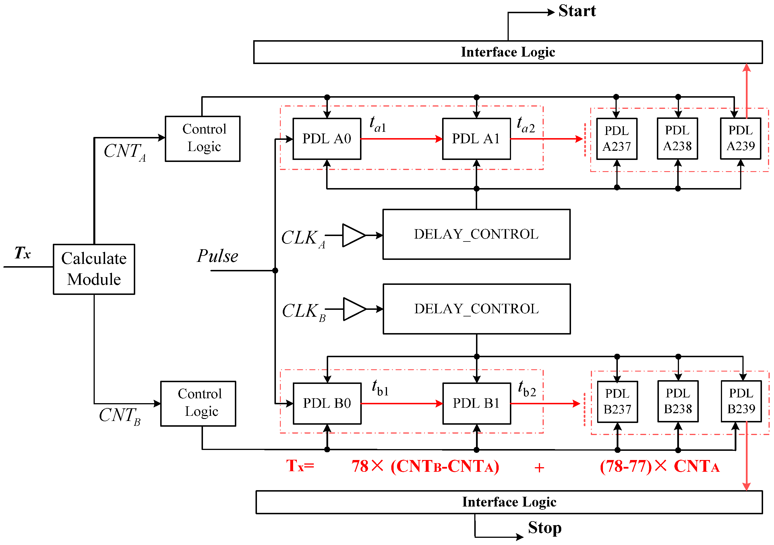
This paper uses a Vernier delay line based on PDLs to realize the DTC. Figure 4 shows the block diagram of the DTC. Two PDL delay lines are built. Each delay line has 240 PDLs, and each PDL has 32 delay taps. A control module controls 40 PDLs, and 12 control modules are used in the two delay lines. CLKA is the reference clock of PDL A0~PDL A239, and CLKB is the reference clock of PDL B0~PDL B239. The frequency of CLKA is 202 MHz and that of CLKB is 200 MHz. Therefore, the resolution of the DTC based on the Vernier delay line realized by PDL is 1 ps, and the dynamic range is 7680 ps.
In order to increase the dynamic range, a modified structure for the DTC is proposed, shown in Figure 5. In the modified design, PDL A0~PDL A236 and PDL B0~PDL B236 act as the first stage delay line (coarse delay line). PDL A237~PDL A239 and PDL B237~PDL B239 act as the second stage delay line (fine delay line). In the first stage delay line, the number of delay taps of PDL A is set to 0. The number of working delay taps of PDL B is set according to Equation (6). As for the second stage, the number of delay taps of PDL A and PDL B are the same, which is represented by CNTB. For a certain time interval Tx, CNTA, and CNTB can be calculated from the equations below. In the modified design, the frequency of CLKA and CLKB are still 202 MHz and 200 MHz. The effective range of the DTC is enlarged to 590 ns.
DTCs available with a large dynamic range are most realized by coarse and fine methods. The coarse method is commonly realized by counting the periods of a clock signal [3,9,10], which is very simple in implementation. However, the counting circuit may introduce additional errors into the circuit and decrease the conversion accuracy, especially the error caused by the trigger of the counter. This paper uses a coarse and fine delay line to increase the dynamic range. The coarse delay line and the fine delay line are the same, except that, in the coarse delay line, the number of working delay taps of PDL A0~PDL A236 is set to 0. By doing this, we increase the dynamic range without decreasing the conversion accuracy.
3. Circuit Implementation
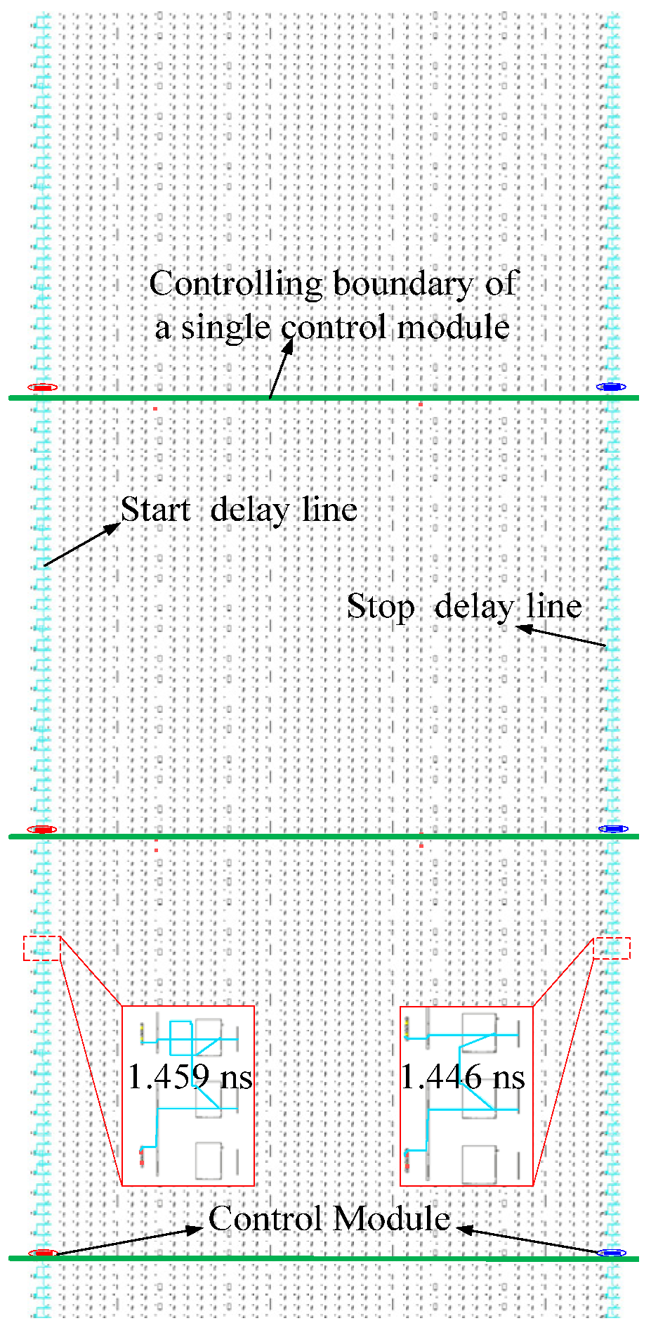
The DTC shown in Figure 5 is implemented in the Xilinx Virtex-6 FPGA chip. Part of the place and route of the Vernier delay line constructed by PDLs is shown in Figure 6. In the figure, the delay line on the left is the Start delay line, and the delay line on the right is the Stop delay line. The cyan lines are the propagation paths between the PDLs. In the figure, 1.459 ns is the path delay between PDL A68 and PDL A69, and 1.446 ns is the path delay between PDL B68 and PDL B69, which corresponds with Figure 7. The control modules of the Start delay line are marked in red, and those of the Stop delay line are marked in blue. The green lines indicate the controlling boundary of a single control module.
One of the most important delays that may affect the performance of the DTC is the delay of propagation paths between the PDLs. The time delay of the propagation paths (ta and tb in Figure 5) is shown in Figure 7a, and the data are obtained from the FPGA editor (a design tool of the Xilinx ISE design suite). In the figure, most of the propagation paths on the Start delay line and the Stop delay line are equal and can be offset. The largest delay difference is 31 ps as shown in Figure 7b. The integral delay difference between the Start delay line and the Stop delay line is 202 ps. The measurement error introduced by the propagation paths is a fixed error and can be compensated.
Another delay is the intrinsic delay of PDL, which is about 400 ps [12,13]. The intrinsic delay indicates the time delay of a PDL when the number of working delay taps is set to 0. For a delay line with 240 PDLs, the intrinsic delay is about 100 ns. However, the intrinsic delay is identical on both lines. In the design shown in Figure 5, the time interval signals (Start and Stop) is generated at the last PDL of the delay lines, which does not need multiplexers to collect and select the output signal. By doing this, the measurement error caused by the intrinsic delay of PDL can be offset completely.
4. Experiments
4.1. Setup of Experiments
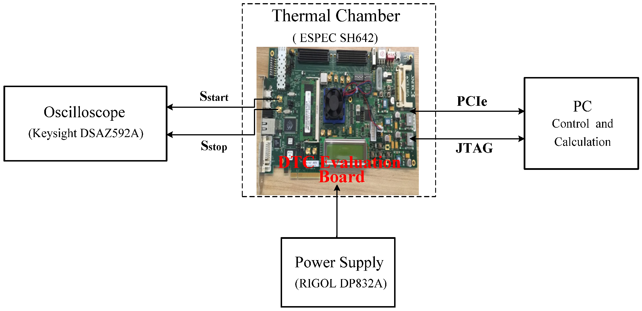
For function verification and performance evaluation, the Xilinx Virtex-6 FPGA chip is adopted for circuit realization. The evaluation board ML605 (designed by Xilinx Inc., San Jose, CA, USA) is used. The reference clock of the board is a crystal oscillator with a frequency of 200 MHz. CLKA and CLKB are generated by the Mixed-Mode Clock Managers (MMCMs), which is realized by multiplying or fractional dividing the reference clock. CLKA and CLKB are connected to global clock buffers, which is a dedicated interconnect network specifically designed to reach all clock inputs of the various resources inside an FPGA chip. These networks feature low skew and low duty cycle distortion, low power, and improved jitter tolerance.
The DTC evaluation board communicates with the PC via PCI (peripheral component interconnect) Express interface. The time interval signal generated is outputted through the SMA (small-motion accelerometer) connector, which has the advantage of low noise. The test system of the DTC is shown in Figure 8. The evaluation board is supplied by RIGOL DP832A (RIGOL Technologies Inc., Beijing, China), and a digital oscilloscope (Keysight DSAZ592A, Keysight Technologies, Santa Rosa, CA, USA) is employed to measure the time interval generated. Additionally, a thermal chamber (ESPEC SH642, designed by ESPEC Corp., Osaka, Japan) is utilized to evaluate the temperature stability of the DTC.
4.2. Analysis of Clock Jitter and Phase Noise
In this paper, CLKA and CLKB are generated by the MMCMs. The input clock is from an oven controlled crystal oscillator (OCXO) with a frequency stability of ±0.3 ppb. In the realization, the MMCM (mixed-mode clock managers) parameter is enabled to minimize output jitter. Experiments are conducted to measure the jitter of CLKA and CLKB. Figure 9 shows the Random Jitter, Period Jitter (RJ, PJ) Histogram of CLKA and CLKB, which is obtained above 6 × 10⁶ transitions. The RJ of CLKA is 8.52 ps, and the PJ of CLKA is 9.79 ps. The RJ of CLKB is 8.92 ps, and the PJ of CLKB is 7.60 ps. Here, all the values are root mean square (RMS) values.
The influence of the jitter on the performance of the proposed DTC is analyzed in two aspects. First, the difference in RJ between CLKA and CLKB is −0.4 ps, and that of PJ is 2.39 ps. The proposed DTC is based on the Vernier delay line structure, which is a symmetrical structure. The clock jitter exists on both of the delay lines. Then, the influence of jitter of CLKA and CLKB on the DTC can be offset by the two delay lines to some degree. Second, the control module of the PDL is a close-loop structure, which can reduce the jitter of the clocks.
The period jitter of CLKA and CLKB is related to the phase noise. The relation between the period jitter and the phase noise can be calculated from Equation (9) [14]. In Equation (9), JPER is the period jitter, fc is the clock frequency, and L(f) is the phase noise spectrum. The period jitter of CLKA and CLKB are shown in Figure 9, and both of them are <10 ps. The phase noise and jitter of CLKA and CLKB can transmit to the control modules of PDL and affect the time delay of delay taps. The largest jitter on tap delay of PDL is ±5 ps [13]. Though the theoretical resolution of the proposed DTC is 1 ps, and the measurement accuracy is lower, which is about 10 ps (RMS value).
4.3. Average Resolution and Nonlinearity Tests
The performance of the Virtex-6 DTC is measured within the range of 0~500 ns. When CNTA and CNTB are both 0, the obtained time interval is 205 ps. When CNTA and CNTB are both 96, the obtained time interval is 303 ps. Therefore, the obtained average resolution is (303 − 205)/96 = 1.02 ps. According to Figure 7, a 202 ps fixed error is introduced by the delay difference between the propagation paths of the Start delay line and the Stop delay line. Therefore, calibration work is done by adding the time delay of the Stop delay line by 205 ps.
The DNL of the delay cells in PDLs are tested and analyzed. The DNL of delay cells in PDL A237~PDL A239 and PDL B237~PDL B239 are shown in Figure 10. The nonlinearity tests are performed in 96 taps. In the tests, we set the number of delay taps within the range of 0~96 and measure the time delay between the input of PDL A237 and the output of PDL A239 through the oscilloscope. The DNL of delay cells can be calculated from the measurement results. The DNL of delay cells in PDL A237~PDL A239 is −0.074~+0.079 LSB (least significant bit, 1 LSB = 77 ps). The DNL of delay cells in PDL B237~PDL B239 is measured with the same method, and the obtained DNL is −0.065~+0.075 LSB (1 LSB = 78 ps). The DNL of delay cells in PDL A237~PDL A239 and PDL B237~PDL B239 indicates the nonlinearity of the delay cells in two PDL delay lines. The largest DNL error is about 6 ps, which is mainly introduced by the jitter of clock signals and the jitter of the control module of PDL.
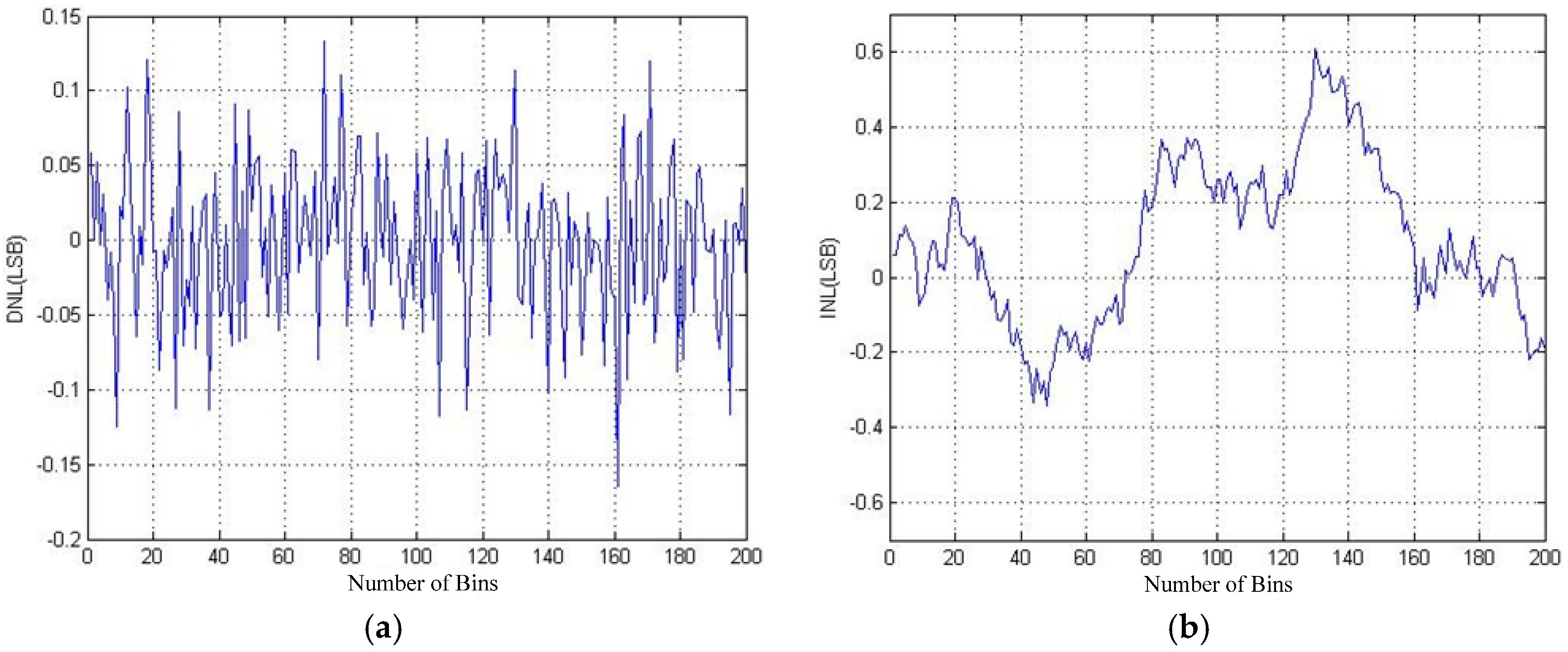
The DNL and INL (integral nonlinearity) of the proposed Virtex-6 FPGA-based DTC are shown in Figure 11. The delay characteristic and the structure of all the PDLs in the delay line are nearly the same. The nonlinearity tests are performed in 200 bins. The DNL is −0.17~+0.13 LSB and the INL is −0.35~+0.62 LSB. The operation range of the proposed DTC is as large as 590 ns. Time intervals larger than 96 ps are generated by increasing the number of delay taps in Line B and have good delay linearity, which is benefited from the structure of the programmable delay line. Therefore, the nonlinearities are measured within the range of 5 ns and can indicate the nonlinearities of the proposed DTC within the operation range.
4.4. Temperature and Voltage Stability Tests
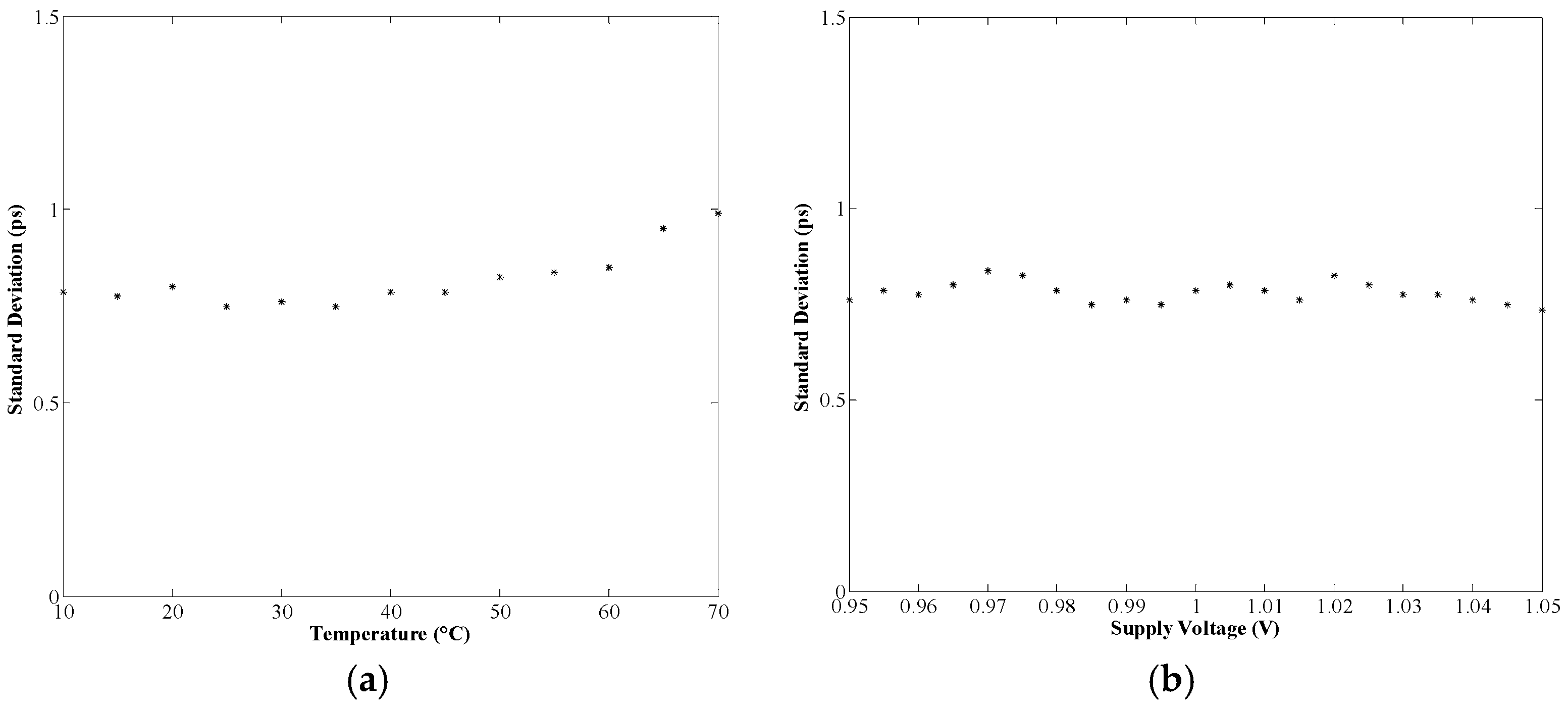
The temperature stability of the proposed DTC is tested on the evaluation board with the help of a thermal chamber. A constant time interval (5 ns) is generated under different temperature, in a range of 10~70 °C. The time interval is measured by the digital oscilloscope, and measurement under a temperature is repeated 50 times. The standard deviation under different temperature is shown in Figure 12a, which indicates that the proposed DTC is less sensitive to variations of temperature when compared with other DTCs implemented in a similar FPGA device [10].
The voltage tests are performed using the DC power supply RIGOL DP832A (RIGOL Technologies Inc., Beijing, China). The nominal operating voltage of the DTC board is 1 V, which is the internal supply voltage of the FPGA device. In the tests, the supply voltage of the FPGA is changed within the range of 0.95~1.05 V with an interval of 5 mV. A constant time interval (5 ns) is generated under different supply voltages at an ambient temperature of 25 °C. The time interval is measured by the digital oscilloscope, and measurement under a temperature is repeated 50 times. The standard deviation of the measurement results is shown in Figure 12b. In the figure, with the change of supply voltage, the largest differences in standard deviation is less than 0.5 ps, which indicates that the proposed DTC is not sensitive to variations of supply voltage.
4.5. Comparison with Other DTCs
Table 1 compares the performance of the proposed DTC with previous work. Compared with other DTCs implemented in an FPGA device, the proposed DTC achieves the best resolution. The dynamic range and the linearity are also good among the DTCs in the table. The jitter and skew of the proposed DTC is larger than ASIC-based DTCs. That is mainly because the circuit and architecture of ASIC-based DTC is fully customized, while the FPGA is commercial and its architecture is not specialized for DTC.
5. Conclusions
This paper presents a novel realization of a DTC based on the principle of the Vernier delay line. The proposed DTC is designed based on a coarse and fine Vernier delay line constructed by PDLs, which are controlled by a closed feedback delay loop and can ensure the linearity and stability of the DTC. The proposed DTC is implemented and tested in the Xilinx FPGA evaluation board. The obtained resolution is 1.02 ps, and the differential nonlinearity and integral nonlinearity of the DTC is −0.17~+0.13 LSB and −0.35~+0.62 LSB, respectively. Compared with other DTCs, the realized DTC is higher in resolution and less sensitive to variations in voltage and temperature.
Acknowledgments
This research is supported by the Fundamental Research Funds for the Central Universities of China (No. JB160409) and the National Science Foundation of China (No. 10703004).
Author Contributions
Hai Wang and Min Zhang conceived and designed the experiments; Min Zhang performed the experiments; Hai Wang and Yan Liu analyzed the data; Yan Liu contributed reagents/materials/analysis tools; Hai Wang and Min Zhang wrote the paper.
Conflicts of Interest
The authors declare no conflict of interest.
References
- Lai, C.M.; Tan, K.W.; Chen, Y.J.; Chu, T.S. A UWB impulse radio timed-array radar with time-shifted direct-sampling architecture in 0.18 µm CMOS. IEEE Trans. Circuits Syst. I Regul. Pap. 2014, 61, 2074–2087. [Google Scholar] [CrossRef]
- Lai, C.M.; Wu, J.M.; Huang, P.C. A scalable direct-sampling broadband radar receiver supporting simultaneous digital multi beam array in 65 nm CMOS. In Proceedings of the 2013 IEEE International Solid-State Circuits Conference Digest of Technical Papers, San Francisco, CA, USA, 17–21 February 2013; pp. 242–243.
- Klepacki, K.; Pawłowski, M.; Szplet, R. Low-jitter wide-range integrated time interval/delay generator based on combination of period counting and capacitor charging. Rev. Sci. Instrum. 2015, 86. [Google Scholar] [CrossRef] [PubMed]
- Wang, T.Y.; Lin, S.M.; Tsao, H.W. Multiple channel programmable timing generators with single cyclic delay line. IEEE Trans. Instrum. Meas. 2004, 53, 1295–1303. [Google Scholar] [CrossRef]
- Chen, P.; Chen, P.Y.; Lai, J.S.; Chen, Y.J. FPGA Vernier Digital-to-Time Converter with 1.58 ps Resolution and 59.3 Minutes Operation Range. IEEE Trans. Circuits Syst. 2010, 57, 1134–1142. [Google Scholar] [CrossRef]
- Vornicu, I.; Carmona-Galán, R.; Rodríguez-Vázquez, A. Wide Range 8ps Incremental Resolution Time Interval Generator based on FPGA technology. In Proceedings of the 21st IEEE International Conference on Electronics, Circuits and Systems (ICECS), Marseille, France, 7–10 December 2014; pp. 395–398.
- Alahdab, S.; Mäntyniemi, A.; Kostamovaara, J. A 12-Bit Digital-to-Time Converter (DTC) with sub-ps-level resolution using current DAC and differential switch for Time-to-Digital Converter (TDC). In Proceedings of the IEEE International Instrumentation and Measurement Technology Conference (I2MTC), Graz, Austria, 13–16 May 2012; pp. 2668–2671.
- Kwiatkowski, P.; Jachna, Z.; Różyc, K.; Kalisz, J. Accurate and low jitter time-interval generators based on phase shifting method. Rev. Sci. Instrum. 2012, 83. [Google Scholar] [CrossRef] [PubMed]
- Vornicu, I.; Carmona-Galán, R.; Rodríguez-Vázquez, A. Time interval generator with 8 ps resolution and wide range for large TDC array characterization. Analog Integr. Circuits Signal Process. 2016, 87, 181–189. [Google Scholar] [CrossRef]
- Yao, Y.; Wang, Z.; Lu, H.; Chen, L.; Jin, G. Design of time interval generator based on hybrid counting method. Nucl. Instrum. Methods Phys. Res. A 2016, 832, 103–107. [Google Scholar] [CrossRef]
- Wang, H.; Zhang, M.; Yao, Q. A New Realization of Time-to-Digital Converters Based on FPGA Internal Routing Resources. IEEE Trans. Ultrason. Ferroelectr. Freq. Control 2013, 60, 1787–1795. [Google Scholar] [CrossRef] [PubMed]
- Xilinx. Virtex-6 FPGA Clocking Resources User Guide. v1.1, Xilinx: San Jose, CA, USA, 2009.
- Xilinx. Virtex-6 FPGA Data Sheet: DC and Switching Characteristics. v3.2, Xilinx: San Jose, CA, USA, 2011.
- Maxim Integrated, Clock (CLK) Jitter and Phase Noise Conversion—Application Note 3359. Available online: http://pdfserv.maxim-ic.com/en/an/AN3359.pdf (accessed on 10 December 2004).
Figure 1.
Schematic of a time-to-digital converter (TDC) based on a Vernier delay line.
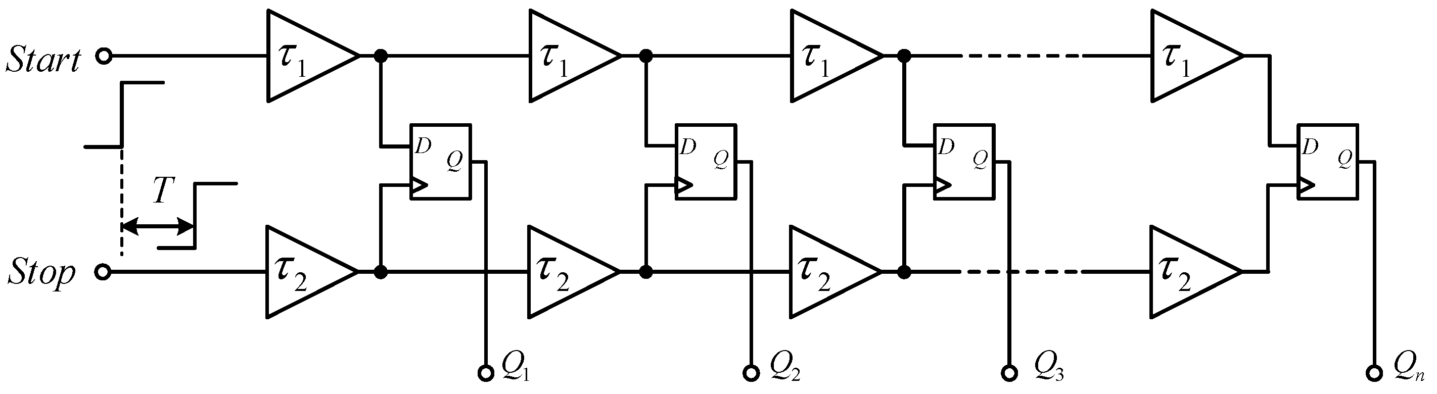
Figure 2.
Schematic of a digital-to-time converter (DTC) based on a Vernier delay line.
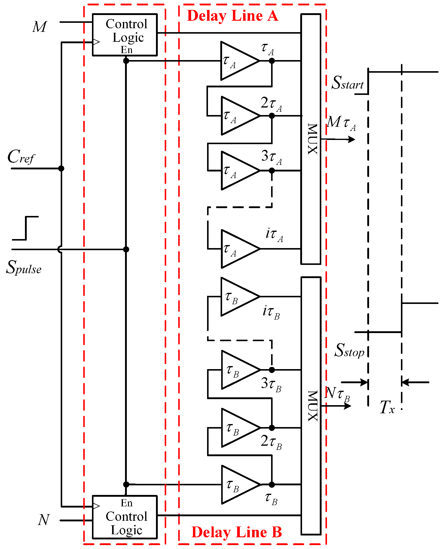
Figure 3.
Schematic diagram of a programmable delay line. (a) Schematic diagram of a PDL (programmable delay line); (b) Schematic diagram of PDL delay lines.
Figure 3.
Schematic diagram of a programmable delay line. (a) Schematic diagram of a PDL (programmable delay line); (b) Schematic diagram of PDL delay lines.

Figure 4.
A simplified block diagram of the proposed DTC.
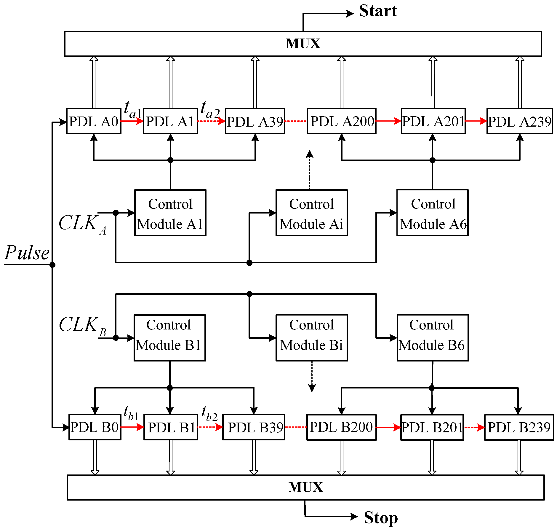
Figure 5.
Modified block diagram of the proposed DTC.

Figure 6.
Place and route of the proposed DTC based on programmable delay lines (PDLs).

Figure 7.
Delay characteristic of the propagation paths. (a) Delay of propagation paths of the two lines; (b) Delay difference between propagation paths of the two lines.
Figure 7.
Delay characteristic of the propagation paths. (a) Delay of propagation paths of the two lines; (b) Delay difference between propagation paths of the two lines.
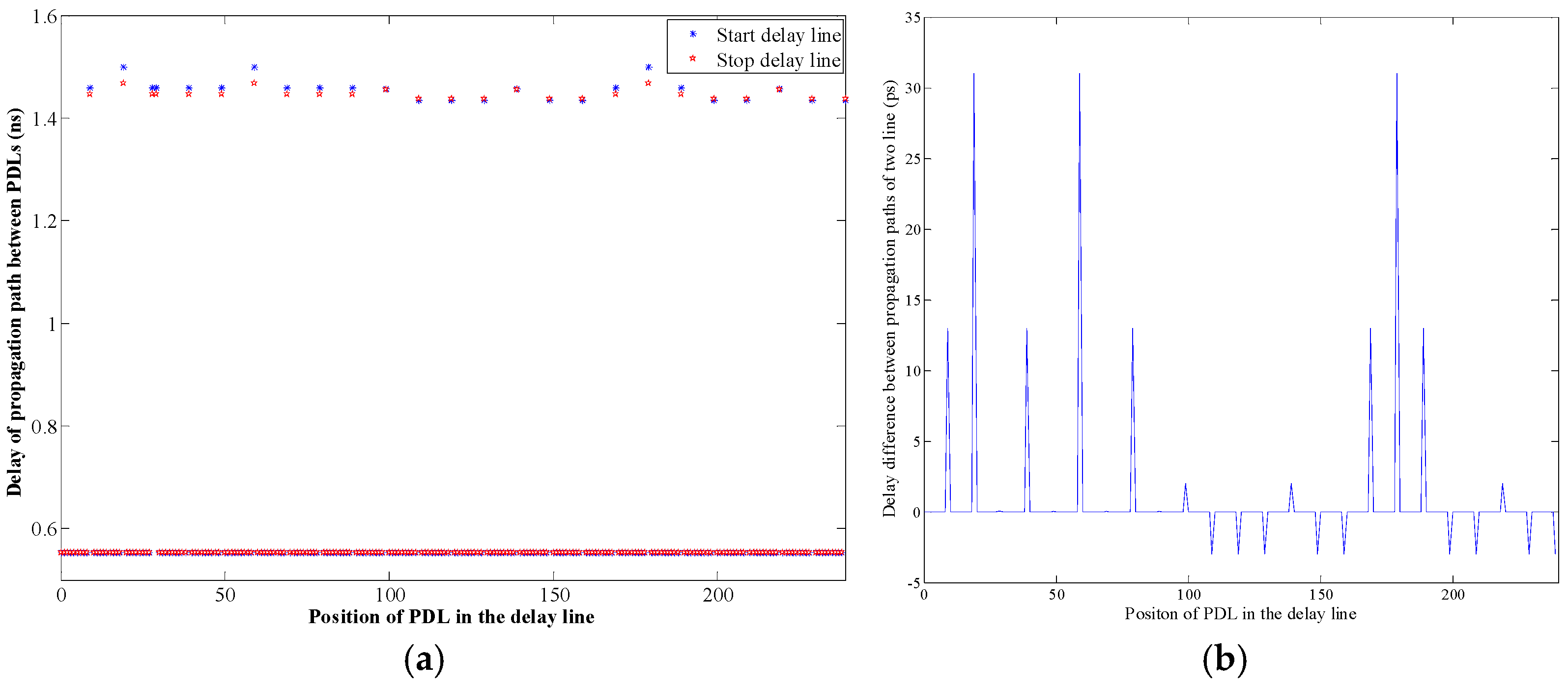
Figure 8.
Test system of the DTC.

Figure 9.
Jitter Histogram of CLKA and CLKB. (a) Jitter of CLKA; (b) Jitter of CLKB.
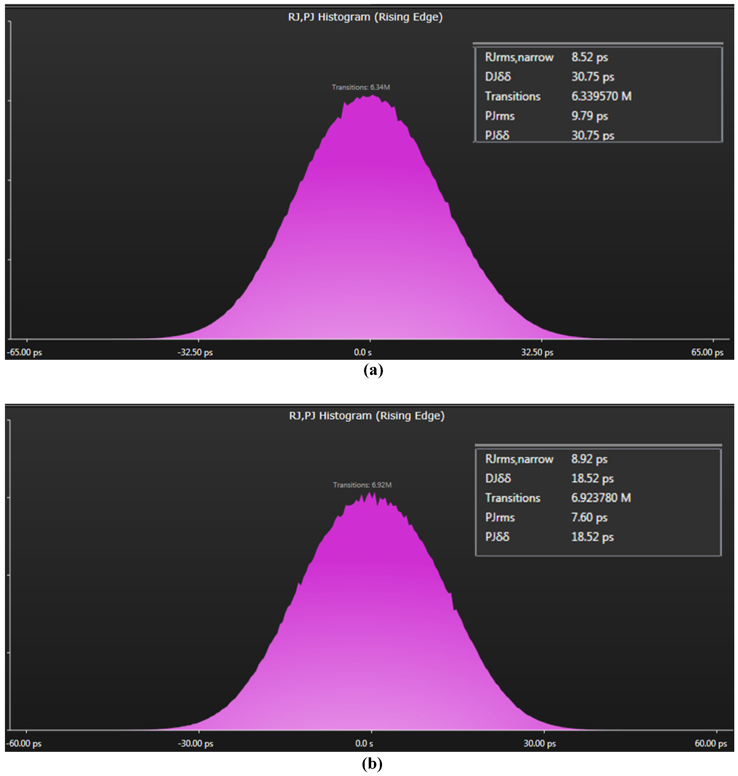
Figure 10.
Differential nonlinearity (DNL) of delay cells in a PDL. (a) DNL of delay cells in PDLA237~PDLA239; (b) DNL of delay cells in PDLB237~PDLB239.
Figure 10.
Differential nonlinearity (DNL) of delay cells in a PDL. (a) DNL of delay cells in PDLA237~PDLA239; (b) DNL of delay cells in PDLB237~PDLB239.
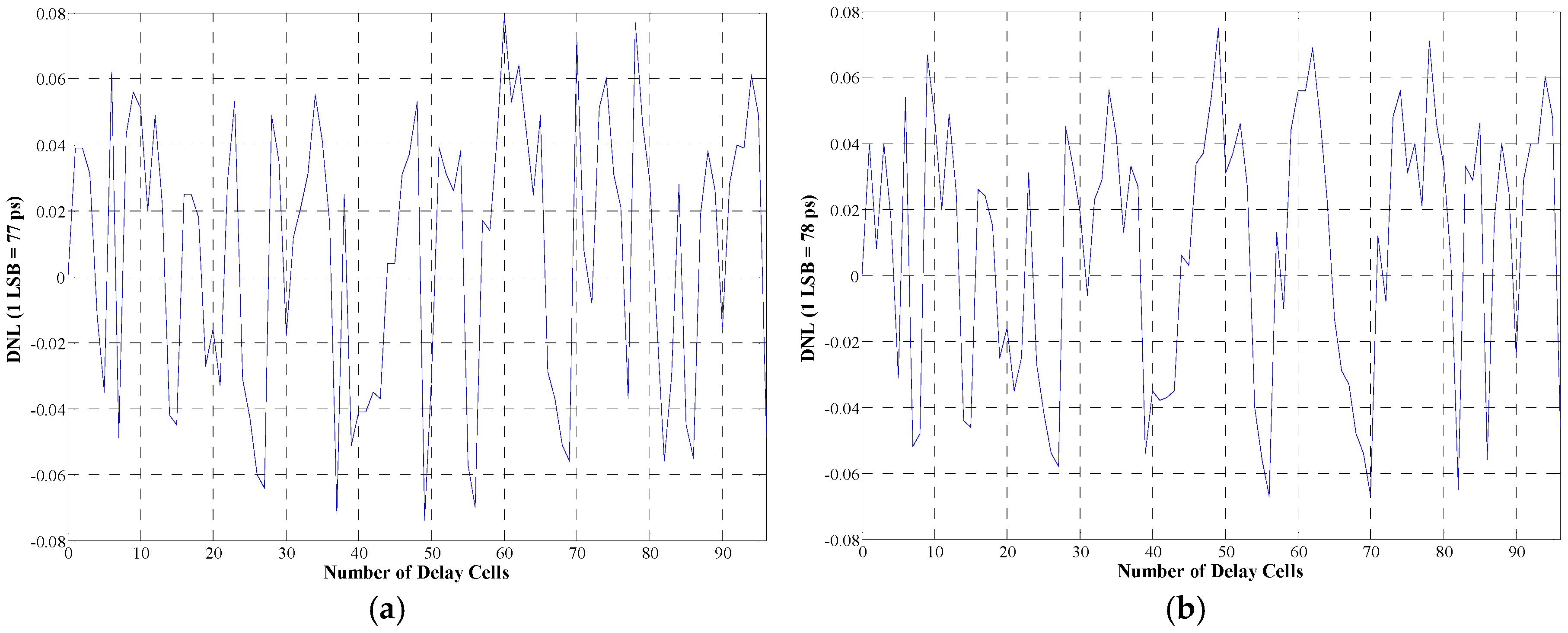
Figure 11.
Nonlinearities of proposed DTC system. (a) DNL; (b) integral nonlinearity (INL).

Figure 12.
(a) Temperature stability of the proposed DTC. (b) Voltage stability of the proposed DTC.
Figure 12.
(a) Temperature stability of the proposed DTC. (b) Voltage stability of the proposed DTC.

| Work | This Work | [1] (2014) | [4] (2004) | [2] (2013) | [5] (2010) |
|---|---|---|---|---|---|
| CMOS 1 Technology | 40 nm FPGA 1 | 0.18 µm ASIC 1 | 0.35 µm ASIC | 65 nm ASIC | 65 nm FPGA |
| Principle | VPDL 1 | Dual PLL 1 | CDL 1 | Dual PLL | Dual PLL |
| Reference Clock | 200 MHz | 625 MHz | 100 MHz | 10 MHz | 1025 MHz |
| Power | 165 mW | 3.3 W | - | 76 mW | 681 mW |
| Resolution | 1.02 ps | 5 ps | 37.5 ps | 6.25 ps | 1.58 ps |
| DNL 1 | −0.17~0.13 LSB | - | −0.6~0.6 LSB | −0.8~1 LSB | - |
| INL 1 | −0.35~0.62 LSB | - | −1~7 LSB | 15 LSB | - |
| Maximum Range | 590.0 ns | 80 ns | 5 ms | 100 ns | 59.3 min |
1 CMOS: complementary metal oxide semiconductor; FPGA: field programmable gate array; ASIC: application specific integrated circuit; VPDL: vernier programmable delay lines; Dual PLL (Phase Locked Loop) is actually a Vernier ring oscillator; CDL: cyclic delay line; DNL: differential nonlinearity; INL: integral nonlinearity.
© 2017 by the authors; licensee MDPI, Basel, Switzerland. This article is an open access article distributed under the terms and conditions of the Creative Commons Attribution (CC-BY) license (http://creativecommons.org/licenses/by/4.0/).
Share and Cite
MDPI and ACS Style
Wang, H.; Zhang, M.; Liu, Y. High-Resolution Digital-to-Time Converter Implemented in an FPGA Chip. Appl. Sci. 2017, 7, 52. https://doi.org/10.3390/app7010052
AMA Style
Wang H, Zhang M, Liu Y. High-Resolution Digital-to-Time Converter Implemented in an FPGA Chip. Applied Sciences. 2017; 7(1):52. https://doi.org/10.3390/app7010052
Chicago/Turabian StyleWang, Hai, Min Zhang, and Yan Liu. 2017. "High-Resolution Digital-to-Time Converter Implemented in an FPGA Chip" Applied Sciences 7, no. 1: 52. https://doi.org/10.3390/app7010052
Note that from the first issue of 2016, this journal uses article numbers instead of page numbers. See further details here.