A Three-Axis Magnetic Field Microsensor Fabricated Utilizing a CMOS Process

1
Department of Mechanical Engineering, National Chung Hsing University, Taichung 402, Taiwan
2
Department of Civil and Environmental Engineering, National University of Kaohsiung, Kaohsiung 811, Taiwan
3
Department of Electro-Optical Engineering, Yuan Ze University, Taoyuan 320, Taiwan
*
Author to whom correspondence should be addressed.
Appl. Sci. 2017, 7(12), 1289; https://doi.org/10.3390/app7121289
Submission received: 17 October 2017
/
Revised: 7 December 2017
/
Accepted: 7 December 2017
/
Published: 11 December 2017
Abstract
:Featured Application
Three-axis magnetic field microsensors in this study can be applied to various electronic instruments, portable electronic devices, mobile phones, and industrial equipment.
Abstract
This study develops a three-axis magnetic field (MF) microsensor manufactured by a complementary metal oxide semiconductor (CMOS) process. The MF microsensor contains a ring emitter, four bases, and eight collectors. Sentaurus TCAD was used to simulate the microsensor characterization. The STI (shallow trench isolation) oxide in the process was used to limit the current direction and reduce leakage current. The microsensor produces a voltage difference once it senses a magnetic field. An amplifier circuitry magnifies voltage difference into a voltage output. Experiments reveals that the MF microsensor has a sensitivity of 1.45 V/T along the x-axis and a sensitivity of 1.37 V/T along the y-axis.
1. Introduction
Many electronic instruments, portable electronic devices, and industrial equipment require magnetic field (MF) sensors [1,2,3,4]. Several transducers have been constructed on a smaller scale by a microelectromechanical system (MEMS) process [5,6,7,8]. Compared with traditional sensors, microsensors are easy to mass produce, are of high quality, are small, and have a low cost [9,10,11,12]. Recently, many MF microsensors have been developed utilizing the MEMS method. For example, Yin et al. [13] made a MEMS torsion oscillator MF sensor. The sensor with a soft magnetic wire was fabricated using a focus ion beam and a MEMS process. The MF sensor could detect a tiny magnetic field. The minimum recognizable magnetic field of the sensor was 55 nT. Zhang et al. [14] fabricated a resonant MF sensor using a MEMS process. The sensor structure was constructed by springs and electrodes. The output signal of the sensor was a variation of resonance frequency. Huang et al. [15] used a CMOS process to fabricate a fluxgate MF microsensor. The sensor was a 3-axis MF designed to detect low magnetic fields and could detect magnetic fields from −3 to 3 mT. Avram et al. [16] made an MF microsensor utilizing a CMOS process. An NPN (n-type, p-type, and n-type silicon) transistor was designed as a 2-axis MF sensor. Song et al. [17] employed a standard CMOS process of Hynix Company to develop an MF microsensor with an NPN transistor on a p-type silicon substrate. Leakage current existed in the sensor because there was no buried layer on the substrate. Yu et al. [18] presented a 2-axis magnetic Hall device based on a bipolar transistor process. The interaction effect of the magnetotransistor and the magnetoresistor in the device was investigated. There were three operation modes for the magnetic device. The magnetic Hall device needed a supply current of 100 mA, so it had a high power consumption problem. Estrada et al. [19] also utilized a bipolar transistor process to develop a magnetic Hall sensor, which had a low sensitivity of 0.02 mV/T. The sensitivity and performance of the sensor [16,17] manufactured by a CMOS process were higher than that manufactured by a bipolar process [19]. These microsensors [16,17,18] made by a CMOS process were 1-axis and 2-axis magnetic sensors. Thereby, a three-axis MF microsensor in this study was developed utilizing a standard CMOS process. Fabrication of the MF sensor in this study was simpler than that of these aforementioned sensors [13,14,15] because the sensor in this work required no added materials and did not involve any post-process.
A CMOS process employed to make various MEMS devices is called a CMOS-MEMS technique [20,21,22]. Many microsensors have been made this way [23,24,25]. In this study, a 3-axis MF microsensor was developed using the CMOS-MEMS technique. Several CMOS-MEMS magnetic microsensors [26,27,28] have required post-processing to obtain suspension components and to add functional materials. The MF sensor in this work did not require any post-processing, and its fabrication was fully consistent with the CMOS process. The design of this MF microsensor adopted an NPN transistor structure. The STI (shallow trench isolation) oxide was adopted to limit the current direction and reduce leakage current. This MF microsensor has a potential for applications in mobile and electronic instruments owing to its small volume and high sensitivity.
2. The Design of Magnetic Field Sensors
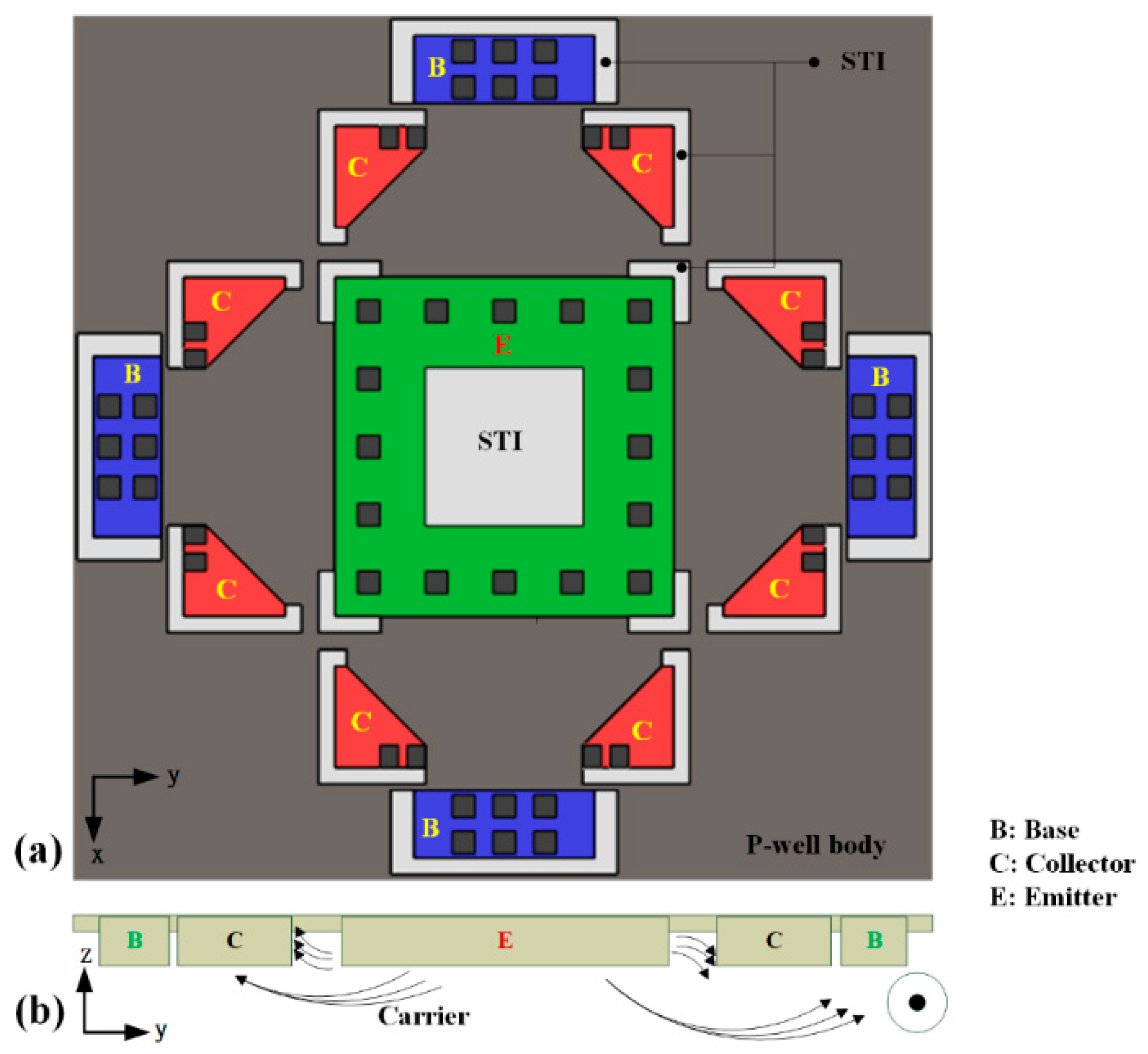
A magnetotransistor mechanism [10] was used to design this 3-axis MF microsensor. Figure 1a demonstrates the three-axis MF microsensor structure. Its structure is composed of a ring emitter, four bases, and eight collectors. The MF microsensor was constructed by an NPN magnetotransistor. As shown in Figure 1a, the STI oxide surrounds the emitter edge to counteract current moving. The STI oxide was also used to decrease the vertical p–n-junction effect and to eliminate the current from the surface of the magnetotransistor. Each electrode links a resistance, so the voltage difference of the bases in the x- and y-directions can be measured.
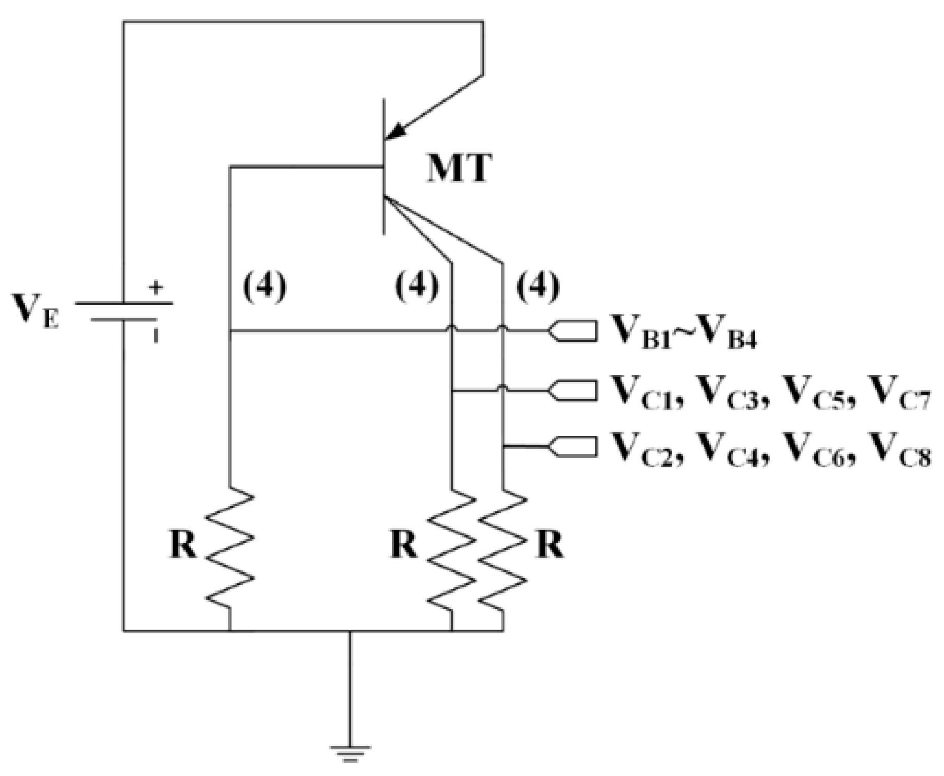
A magnetotransistor depends on the Hall effect. Figure 1b presents a cross-sectional view of the MF microsensor. Carriers, giving a magnetic field in the x-direction, move from the emitter to the collectors and bases. On the right in Figure 1b, the path of the carriers is bent downward by Lorentz force when carriers move to the right collector, and they move across the right collector to the right base, leading to the right base current increment. On the left of Figure 1b, the path of the carriers is bent upward by Lorentz force when carriers move to the left collector, and they are difficult to move across the left collector to the left base, leading to the left base current decrement. Thereby, this action causes both the right and left bases in the y-direction to generate a voltage difference. Similarly, the bases in the x-direction produce a voltage difference when a magnetic field is given in the y-direction. In both collectors, the current causes an imbalance when a magnetic field is given in the z-direction, so both collectors generate a voltage difference. Figure 2 illustrates an equivalent circuit for the microsensor, where MT denotes the magnetotransistor, VE is the bias voltage of the emitter, VB1, VB2, VB3, and VB4 are the voltages of the bases, VC1, VC2, VC3, VC4, VC5, VC6, VC7, and VC8 are the voltages of the collectors, R is the resister, and the symbol (4) represents the related circuit repeated four times. The resistor R is 1 kΩ. When the magnetic field in the x-direction applies to MT, we can measure a voltage difference between bases VB2 and VB4. Relatively, the magnetic field in the y-direction supplies to MT, and the voltage difference between bases VB1 and VB3 is then acquired. Finally, the voltage difference between collectors VC1 and VC3 (or VC2/VC4) is yielded when the magnetic field in the z-direction supplies to MT.
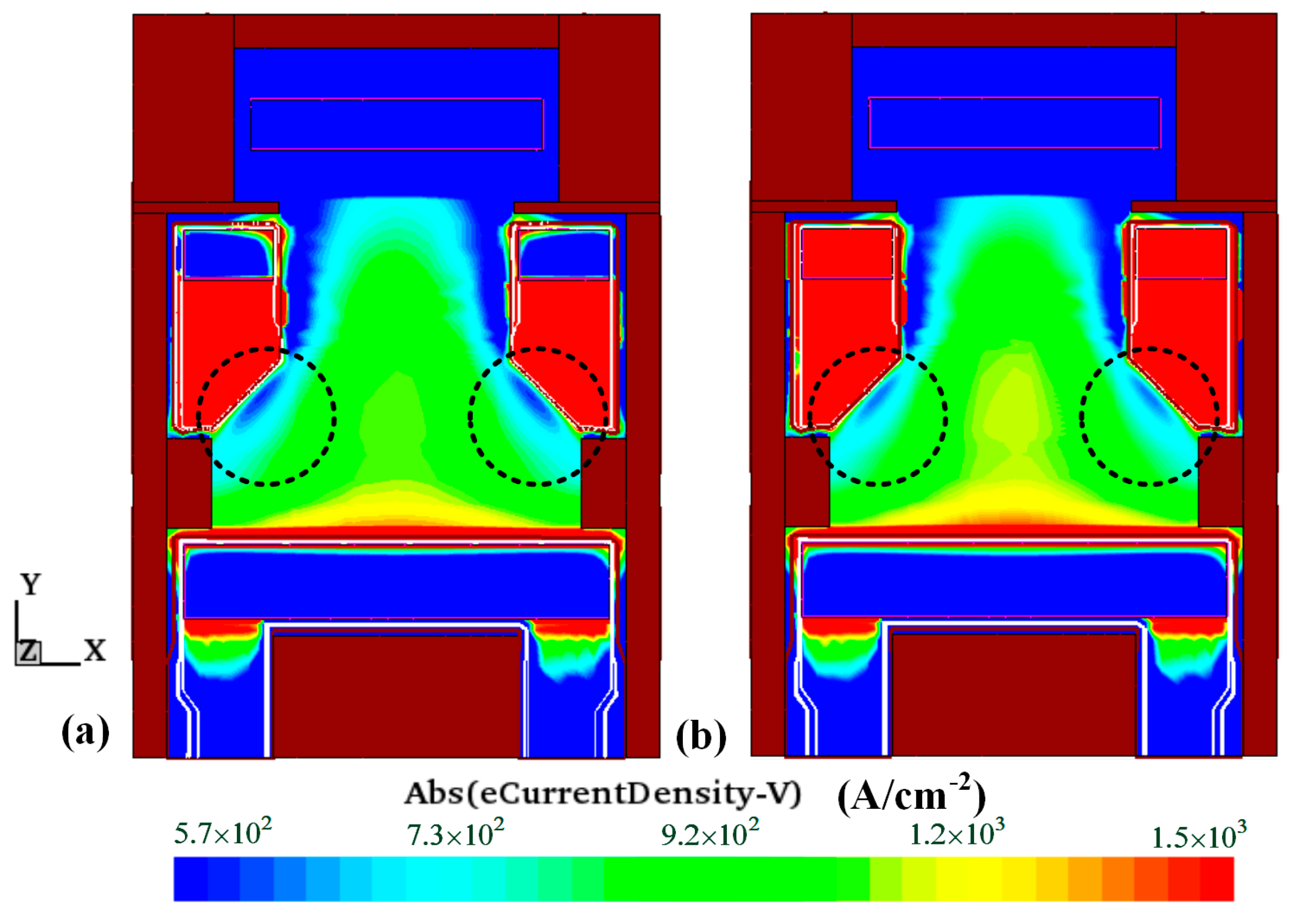
Carrier motion in the MF microsensor was simulated using FEM (finite element method) software Sentaurus TCAD. The MF microsensor is a symmetrical structure, so only one-quarter of the MF microsensor is established to reduce model size and simulation time. The model is meshed using the Delaunay triangulation method, and the model has 4 × 10⁶ elements. The coupling effect of the electrical and magnetic fields is evaluated utilizing the Poisson electron hole approach. The carrier density of the MF microsensor model is computed by solving with the Bank/Rose approach. Figure 3 illustrates the computed results of the surface carrier density distribution for the MF microsensor model with the x-direction MF. The surface carrier density distribution of the MF microsensor without a magnetic field is presented in Figure 3a, and the surface carrier density distribution of the MF microsensor with 200 mT in the x-direction MF is presented in Figure 3b. In this computation, the emitter needs to supply a current and a bias voltage. The current and bias voltage for the emitter are 4 mA and 1.8 V, respectively. As shown in Figure 3a,b, we know that the base current increases by 930 nA at 200 mT in the x-direction MF by comparison of the computations.
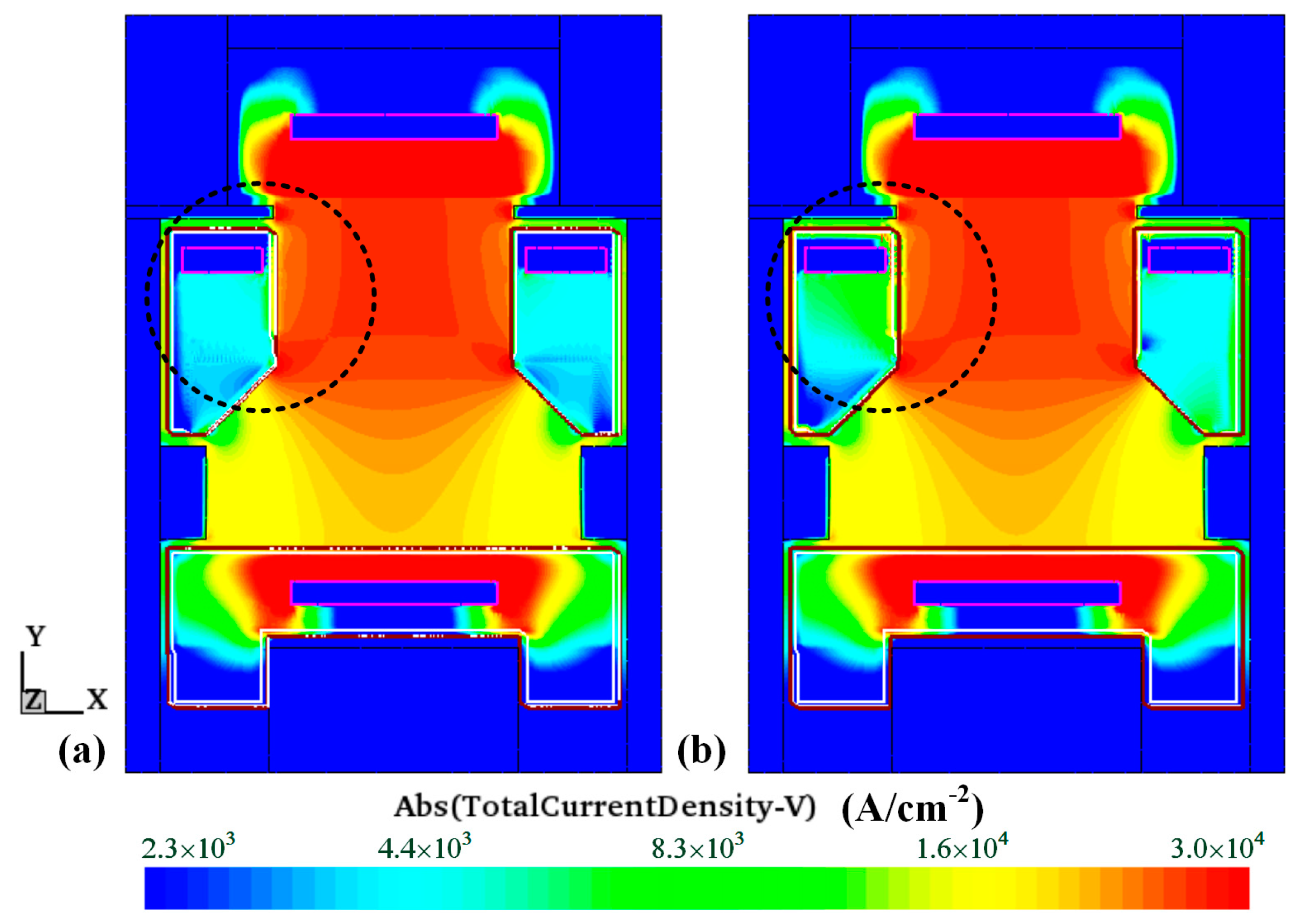
With the same computation method, surface carrier density distribution in the z-direction MF for the microsensor was evaluated. The emitter requires a bias voltage and a current. The bias voltage and current applied to the emitter were 1.8 V and 4 mA, respectively. Figure 4 illustrates the evaluated results of the surface carrier density distribution for the MF microsensor in the z-direction MF. The surface carrier density distribution of the MF microsensor without a magnetic field is illustrated in Figure 4a, and the surface carrier density distribution of the MF microsensor with 200 mT in the z-direction MF in Figure 4b. As shown in Figure 4a,b, the current of the left collector increases by 90 nA at 200 mT in the z-direction MF.
To characterize the relation between the output signal and the magnetic field, the output voltage of the bases in the x-direction MF was evaluated using TCAD. The bias voltage and current applied to the emitter in this evaluation were 1.8 V and 4 mA, respectively. The magnetic field changed from −200 to 200 mT in the x-direction. Figure 5 shows the evaluated voltage difference of the bases in the x-direction MF. As shown in Figure 5, the voltage difference of the bases was −1.3 mV at −200 mT, and this value changed to 1.3 mV at 200 mT. The slope of the curve in Figure 5 is 6.5 mV/T. Because the MF microsensor is a symmetric structure, the voltage difference of the bases in the y-direction MF is the same as that in the x-direction MF.
To understand the MF microsensor performance in the z-direction MF, it was analyzed with the same method. The evaluation of voltage difference for collectors in the z-direction magnetic field is presented in Figure 6. The results depict that the voltage difference of the collector was −0.08 mV at −200 mT, and the value increased to 0.08 mV at 200 mT. The slope of the curve in Figure 6 is 0.4 mV/T.
As shown in Figure 5 and Figure 6, the slope of the curve (Figure 5) is 6.5 mV/T, and the slope value (Figure 6) is 0.4 mV/T. Therefore, the output signals of the bases and collectors in the MF microsensor were not large. To magnify the output signal of the MF microsensor, an amplifier circuitry was utilized to enlarge the output signal of the MF microsensor. Figure 7 shows the amplifier circuitry of the MF microsensor, where Vin denotes the MF sensor voltage difference, and V0 is the amplifier circuitry output voltage. The amplifier circuitry contains six resistors and two amplifiers. The first stage amplifier of A1 enlarges the voltage difference of Vin and eliminates the initial offset of the sensor. Then, the second stage amplifier of A2 strengthens the amplifier A1 output voltage. The output voltage of the amplifier circuitry can be expressed as [29]
where Ra, Rb, Rc, and Rd denote resistors as shown in Figure 7. According to Equation (1), we can match the resistors to obtain an ideal magnification effect.
The resistors Ra, Rb, Rc and Rd in this evaluation are 1, 50, 5 and 25 kΩ, respectively. Substituting the resister values into Equation (1), we know that the gain of circuitry is 250. To understand the magnification effect of the amplifier circuitry for the microsensor sensing signal in the x-direction MF, the voltage difference of the bases in Figure 5 and the resisters (Ra = 1 kΩ, Rb = 50 kΩ, Rc = 5 kΩ, Rd = 25 kΩ) are substituted into Equation (1), and the output voltage of the microsensor is then yielded. The evaluated output voltage of the MF microsensor with amplifier circuitry is presented in Figure 8. The evaluated results depict that the output voltage of the MF microsensor with amplifier circuitry was −0.33 V at −200 mT, and this value changed to 0.33 V at 200 mT. The slope of curve in Figure 8 is 1.63 V/T, which is the evaluated sensitivity of the microsensor with amplifier circuitry in the x-direction MF.
The microsensor is a symmetric structure, so its output signal and sensing performance in the x- and y-directions were the same. Therefore, the evaluated results in Figure 8 were also applied to the microsensor with amplifier circuitry in the y-direction MF. The evaluated sensitivity of the microsensor with amplifier circuitry in the y-direction MF was also 1.63 mV/T.
To realize the signal magnification of amplifier circuitry for the microsensor in the z-direction MF, the voltage difference of the collectors in Figure 6 and the resisters (Ra = 1 kΩ, Rb = 50 kΩ, Rc = 5 kΩ, Rd = 25 kΩ) are substituted into Equation (1), and the output voltage of the microsensor can then be obtained. Figure 9 plots the evaluated output voltage of the microsensor with amplifier circuitry in the z-direction MF. As shown in Figure 9, the output voltage of the MF microsensor with amplifier circuitry was −0.02 V at −200 mT, and the value increased to 0.02 V at 200 mT. The slope of the curve in Figure 9 is 0.1 V/T, which is the evaluated sensitivity of the microsensor with amplifier circuitry in the z-direction MF.
3. Fabrication of Magnetic Field Sensor
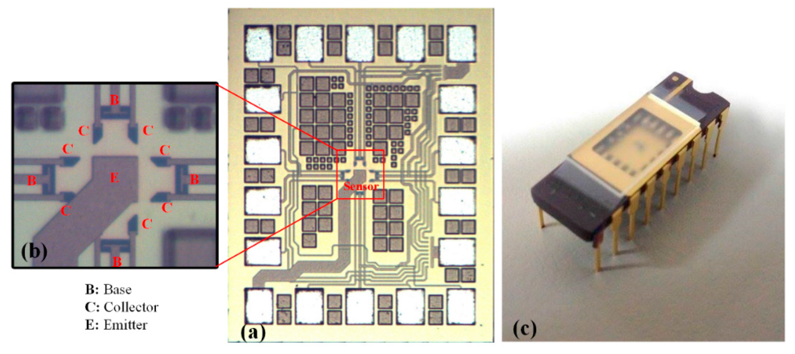
A standard 0.18 μm CMOS process of Taiwan Semiconductor Manufacturing Company (TSMC) was utilized to make the MF microsensor [10]. According to the MF microsensor model in Figure 1, we designed the layout of the MF microsensor. The microsensor layout had to fit the design rules of TSMC. The chip of the MF microsensor was thus fabricated utilizing the CMOS process in accordance with the sensor layout. Figure 10a demonstrates an image of the MF microsensor chip after the CMOS process. The microsensor did not require any post-processing, so its fabrication was simpler than other MEMS magnetic field microsensor [16,17,18]. Figure 10b illustrates a magnification of the MF microsensor. As illustrated in Figure 10b, the microsensor contained a ring emitter, four bases, and eight collectors. The emitter was n-type silicon doped with phosphorus. The bases were p-type silicon doped with boron. The collectors were constructed out of n-type silicon doped with phosphorus. The STI oxide is utilized to decrease leakage current and confine current direction, and it surrounded the emitter edge to limit current moving. The STI oxide was also utilized to eliminate vertical p–n-junction effects. Finally, the MF microsensor chip was packaged, and it was wire-bonded on a frame. Figure 10c demonstrates the MF microsensor image after packaging.
4. Results
The MF microsensor characteristics were measured using a magnetic testing system. The system contained an MF detector, a magnetic field generator, and an oscilloscope. The function of a magnetic generator produced an MF supplied to the microsensor. The MF detector calibrated the magnitude of the MF generated by magnetic generator. The MF microsensor output signal was measured with an oscilloscope.
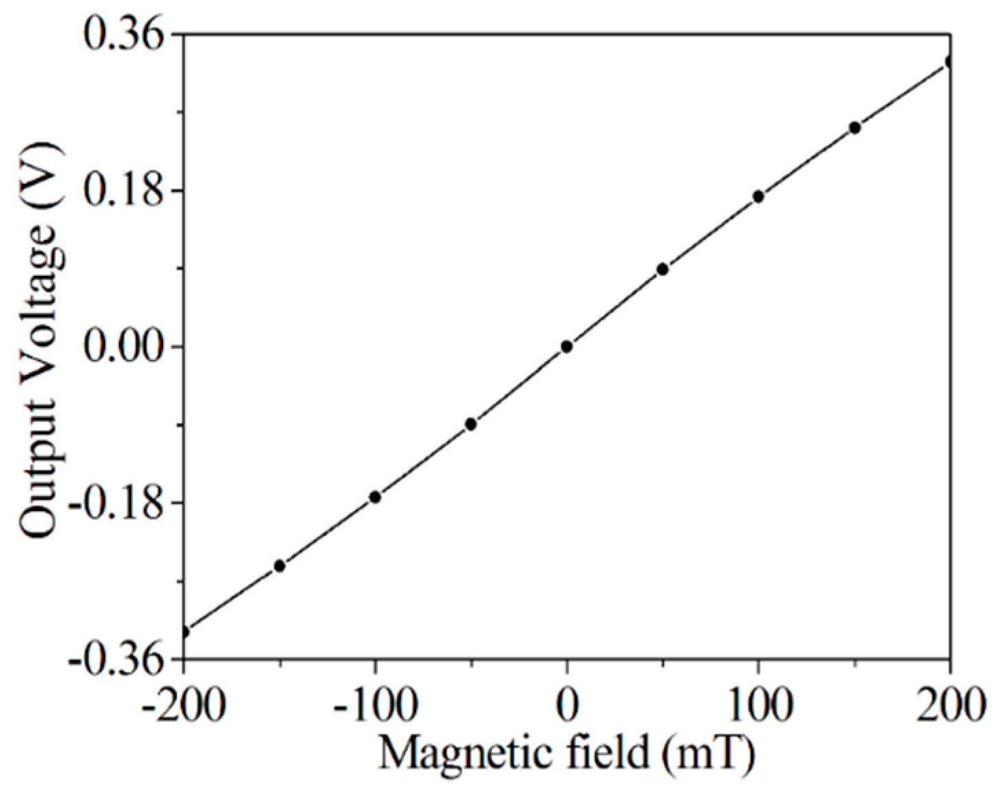
To characterize the MF microsensor with amplifier circuitry, its performances were tested. The MF microsensor was set in the magnetic testing system. A 4 mA current and a 1.8 V voltage were applied to the microsensor. The magnetic field generator supplied an MF range of −200–200 mT to the microsensor, and MF intensity was detected utilizing the MF detector. First, a magnetic field in the x-direction was applied to the microsensor. The oscilloscope was used to measure the output voltage of the microsensor. The sensing response of the microsensor in the x-direction MF was recorded. Figure 11 illustrates the measured output voltage versus the applied magnetic field in the x-direction. As depicted in Figure 11, the microsensor output voltage was −0.17 mV at −100 mT and 0.171 at 100 mT. The results depicted that the microsensor output voltage varied from −0.289 at −100 mT to 0.29 mV at 200 mT. The slope of the curve in Figure 11 was about 1.45 V/T, which was the measured sensitivity of the MF microsensor with amplifier circuitry in the x-direction MF. The microsensor power consumption was 7.2 mW.
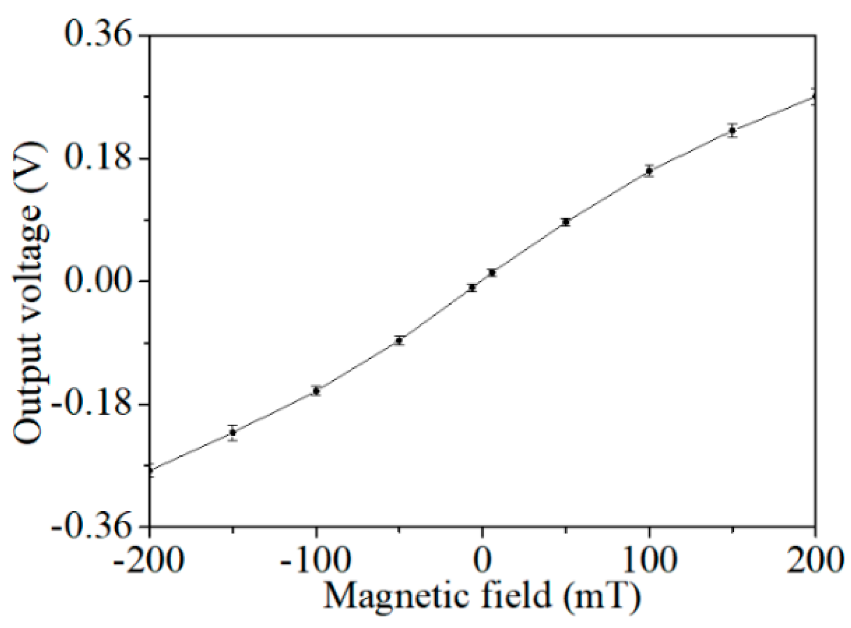
To understand the sensing performance of the microsensor with amplifier circuitry in the y-direction MF, the microsensor was tested with the same approach. The magnetic field was applied to the microsensor in the y-direction, and the microsensor output voltage was measured with an oscilloscope. The sensing response of the microsensor in the y-direction MF was measured. Figure 12 illustrates the measured output voltage versus the applied magnetic field in the y-direction. As presented in Figure 12, the microsensor output voltage was −0.16 mV at −100 mT and 0.161 at 100 mT. The microsensor output voltage changed from −0.277 at −200 mT to 0.271 mV at 200 mT. Therefore, the measured sensitivity of the microsensor with amplifier circuitry in the y-direction MF was 1.37 V/T.
The characteristics of the microsensor with amplifier circuitry in the z-direction MF was also tested. The magnetic field was supplied to the microsensor in the z-direction, and the oscilloscope was used to record the microsensor output voltage. The sensing response of the microsensor in the z-direction MF was recorded. Figure 13 depicts measured output voltage versus applied magnetic field in the z-direction. As illustrated in Figure 13, the microsensor output voltage was −0.017 mV at −100 mT and 0.016 mV at 100 mT. The microsensor output voltage varied from −0.035 at −200 mT to 0.03 mV at 200 mT. Therefore, the measured sensitivity of the microsensor with amplifier circuitry in the z-direction MF was 0.163 V/T.
As depicted in Figure 8, the evaluated sensitivity of the microsensor in the x-direction MF was 1.65 V/T. The measurement results in Figure 11 indicate that the measured sensitivity of the microsensor in the x-direction MF was 1.45 V/T. Comparing evaluation and measurement, the sensitivity of the microsensor in the x-direction MF has an error percentage of 12%. The microsensor structure is a symmetric, so the characteristic of the microsensor in the x- and y-directions MF should the same. In fact, the measurement results in Figure 12 revealed that the microsensor sensitivity in the y-direction MF was 1.37 V/T. The microsensor sensitivity in the x- and y-directions MF has little difference, resulting from the deviation of fabrication and packaging. The measurement results in Figure 13 showed that the microsensor sensitivity in the z-direction MF was 0.163 V/T. Therefore, the microsensor along the x- and y-axes was more sensitive than that in the z-axis.
A Hall MF microsensor proposed by Estrada et al. [19] had a sensitivity of 0.02 mV/T. Leepattarapongpan et al. [30] developed an MF microsensor with a 110 mV/T sensitivity. Tseng et al. [10] made an MF microsensor whose sensitivity was 354 mV/T. The sensitivity of the MF microsensor in this work was higher than those of all three of these studies. The evaluated results in Figure 5 and Figure 6 show that the microsensor is linear output. In fact, the measured results in Figure 11, Figure 12 and Figure 13 show that the microsensor with circuits has little nonlinear output. The reason is that the sensor and circuits are not integrated on-chip, which results in noise and interference.
5. Conclusions
A three-axis MF microsensor was implemented utilizing a standard CMOS technology. Fabrication of the MF microsensor without any post-processing was simpler than that of other MEMS MF microsensors [16,17,18]. In the MF microsensor design, the STI oxide was adopted to surround the emitter edge to counteract current moving and decrease the vertical p–n-junction effect, eliminating the current from the magnetotransistor surface and reducing leakage current. The voltage difference of the bases and collectors in the MF microsensor was not large. Amplifier circuitry was employed to enlarge the output signal of the MF microsensor. The experiments revealed that the MF microsensor had a sensitivity of 1.45 V/T along the x-axis, a sensitivity of 1.37 V/T along the y-axis, and a sensitivity of 0.163 V/T along the z-axis.
Acknowledgments
The authors would like to thank the National Science Council of R.O.C. for financially supporting this research under Contract Nos. MOST 105-2221-E-005-037-MY3 and MOST 106-2221-E-005-050-MY2.
Author Contributions
Jian-Zhi Tseng carried out the fabrication and measurement of the magnetic field microsensor. Po-Jen Shih evaluated the performance of the microsensor. Cheng-Chih Hsu designed the amplifier circuitry for the magnetic field microsensor. Ching-Liang Dai supervised the work of Jian-Zhi Tseng and wrote the paper. All authors read and approved the final manuscript.
Conflicts of Interest
The authors declare no conflict of interest.
References
- Bouvier, B.; Duprey, S.; Claudon, L.; Dumas, R.; Savescu, A. Upper Limb kinematics using inertial and magnetic sensors: Comparison of sensor-to-segment calibrations. Sensors 2015, 15, 18813–18833. [Google Scholar] [CrossRef] [PubMed]
- Brugger, S.; Paul, O. Field-concentrator-based resonant magnetic sensor with integrated planar coils. J. Microelectromech. Syst. 2009, 18, 1432–1443. [Google Scholar] [CrossRef]
- García, A.; Morón, C.; Tremps, E. Magnetic sensor for building structural vibrations. Sensors 2014, 14, 2468–2475. [Google Scholar] [CrossRef] [PubMed]
- Ali, E.; Memari, A.R. Effects of Magnetic Field of Power Lines and Household Appliances on Human and Animals and Its Mitigation. In Proceedings of the 2010 IEEE Middle East Conference on Antennas and Propagation (MECAP), Cairo, Egypt, 20–22 October 2010; pp. 1–7. [Google Scholar]
- Lu, C.C.; Huang, J. A 3-axis miniature magnetic sensor based on a planar fluxgate magnetometer with an orthogonal fluxguide. Sensors 2015, 15, 14727–14744. [Google Scholar] [CrossRef] [PubMed]
- Kao, P.H.; Dai, C.L.; Hsu, C.C.; Lee, C.Y. Fabrication and characterization of a tunable In-plane resonator with low driving voltage. Sensors 2009, 9, 2062–2075. [Google Scholar] [CrossRef]
- Dai, C.L.; Peng, H.J.; Liu, M.C.; Wu, C.C.; Hsu, H.M.; Yang, L.J. A micromachined microwave switch fabricated by the complementary metal-oxide semiconductor post-process of etching silicon dioxide. Jpn. J. Appl. Phys. 2005, 44, 6804–6809. [Google Scholar] [CrossRef]
- Dennis, J.O.; Ahmad, F.; Khir, M.H.B.M.; Hamid, N.H.B. Optical characterization of Lorentz force based CMOS-MEMS magnetic field sensor. Sensors 2015, 15, 18256–18269. [Google Scholar] [CrossRef] [PubMed]
- Gardner, J.W.; Varadan, V.K.; Awadelkarim, O.O. Microsensors MEMS and Smart Devices; John Wiley & Son Ltd.: Chichester, UK, 2001. [Google Scholar]
- Tseng, J.Z.; Wu, C.C.; Dai, C.L. Modeling and manufacturing of a micromachined magnetic sensor using the CMOS process without any post-process. Sensors 2014, 14, 6722–6733. [Google Scholar] [CrossRef] [PubMed] [Green Version]
- Wattanasarn, S.; Matsumoto, K.; Shimoyama, I. 3D Lorentz force Magnetic Sensor Using Ultra-Thin Piezoresistive Cantilevers. In Proceedings of the 2013 IEEE 26th International Conference on Micro Electro Mechanical Systems (MEMS), Taipei, Taiwan, 20–24 January 2013; pp. 693–696. [Google Scholar]
- Dai, C.L.; Tai, Y.W.; Kao, P.H. Modeling and fabrication of micro FET pressure sensor with Circuits. Sensors 2007, 7, 3386–3398. [Google Scholar] [CrossRef] [PubMed]
- Yin, X.; Jiao, Q.; Yuan, L. MEMS torsion oscillator magnetic field sensor. IEEE Trans. Magn. 2013, 49, 3890–3892. [Google Scholar] [CrossRef]
- Zhang, W.; Lee, J.E.Y. Characterization and model validation of a micromechanical resonant magnetic field sensor. In Proceedings of the 17th International Conference on Solid-State Sensors, Actuators and Microsystems, Barcelona, Spain, 16–20 June 2013; pp. 1859–1862. [Google Scholar]
- Huang, W.S.; Lu, C.C.; Jeng, J.T. A novel 3D CMOS micro-fluxgate magnetic sensor for low magnetic field detection. In Proceedings of the IEEE Sensors, Waikoloa, HI, USA, 1–4 November 2010; pp. 1791–1794. [Google Scholar]
- Avram, M.; Neagoe, O. Bipolar magnetic microsensor for longitudinal fields. Sens. Actuators A 2004, 110, 259–263. [Google Scholar] [CrossRef]
- Song, Y.G.; Ryu, J.G. Fabrication and characteristics of the suppressed sidewall injection magnetotransistor using a CMOS process. Sens. Actuators A 2006, 130–131, 99–104. [Google Scholar] [CrossRef]
- Yu, C.P.; Sung, G.M. Two-dimensional folded CMOS Hall device with interacting lateral magnetotransistor and magnetoresistor. Sens. Actuators A 2012, 182, 6–15. [Google Scholar] [CrossRef]
- Estrada, H.V. A MEMS-SOI 3D-magnetic field sensor. In Proceedings of the 2011 IEEE 24th International Conference on Micro Electro Mechanical Systems (MEMS), Cancun, Mexico, 23–27 January 2011; pp. 664–667. [Google Scholar]
- Wang, Y.T.; Hu, Y.C.; Chu, W.C.; Chang, P.Z. The fringe-capacitance of etching holes for CMOS-MEMS. Micromachines 2015, 6, 1617–1628. [Google Scholar] [CrossRef]
- Dai, C.L.; Chiou, J.H.; Lu, M.S.C. A maskless post-CMOS bulk micromachining process and its application. J. Micromech. Microeng. 2005, 15, 2366–2371. [Google Scholar] [CrossRef]
- Cheng, Y.C.; Dai, C.L.; Lee, C.Y.; Chen, P.H.; Chang, P.Z. A circular micromirror array fabricated by a maskless post-CMOS process. Microsyst. Technol. 2005, 11, 444–451. [Google Scholar] [CrossRef]
- Huang, J.Q.; Li, F.; Zhao, M.; Wang, K. A surface micromachined CMOS MEMS humidity sensor. Micromachines 2015, 6, 1569–1576. [Google Scholar] [CrossRef]
- Yang, M.Z.; Dai, C.L.; Lin, W.Y. Fabrication and characterization of polyaniline/PVA humidity microsensors. Sensors 2011, 11, 8143–8151. [Google Scholar] [CrossRef] [PubMed]
- Dai, C.L.; Chen, Y.C.; Wu, C.C.; Kuo, C.F. Cobalt oxide nanosheet and CNT micro carbon monoxide sensor integrated with readout circuit on chip. Sensors 2010, 10, 1753–1764. [Google Scholar] [CrossRef] [PubMed]
- Beroulle, V.; Bertrand, Y.; Latorre, L.; Nouet, P. Monolithic piezoresistive CMOS magnetic field sensors. Sens. Actuators A Phys. 2003, 103, 23–32. [Google Scholar] [CrossRef]
- Skucha, K.; Gambini, S.; Liu, P.; Megens, M.; Kim, J.; Boser, B.E. Design Considerations for CMOS-Integrated Hall-Effect Magnetic Bead Detectors for Biosensor Applications. J. Microelectromech. Syst. 2013, 22, 1327–1338. [Google Scholar] [CrossRef] [PubMed]
- Lu, C.C.; Liu, Y.T.; Jhao, F.Y.; Jeng, J.T. Responsivity and noise of a wire-bonded CMOS micro-fluxgate sensor. Sens. Actuators A Phys. 2012, 179, 39–43. [Google Scholar] [CrossRef]
- Sedra, A.S.; Smith, K.C. Microelectronic Circuits; Oxford University Press: New York, NY, USA, 1998. [Google Scholar]
- Leepattarapongpan, C.; Penpondee, N.; Phetchakul, T.; Phengan, W.; Chaowicharat, E.; Hruanun, C.; Poyai, A. Merged Three-Terminal Magnetotransistor Based on the Carrier Recombination-Deflection Effect. In Proceedings of the 2008 IEEE Sensors, Lecce, Italy, 26–29 October 2008; pp. 399–402. [Google Scholar]
Figure 1.
The MF microsensor structure: (a) tap view; (b) cross-sectional view.

Figure 2.
Equivalent circuit of the MF microsensor.

Figure 3.
MF microsensor carrier density with (a) 0 mT and (b) 200 mT in the x-direction MF.

Figure 4.
Carrier density of the MF microsensor with (a) 0 mT and (b) 200 mT in the z-direction MF.

Figure 5.
Voltage difference of bases in x-direction MF.

Figure 6.
Voltage difference of collectors in the z-direction MF.

Figure 7.
Amplifier circuitry.

Figure 8.
Evaluated output voltage in the x-direction MF.

Figure 9.
Evaluated output voltage in the z-direction MF.

Figure 10.
The MF microsensor image: (a) chip; (b) magnification; (c) packaging.

Figure 11.
Measured output voltage in the x-direction MF.

Figure 12.
Measured output voltage in the y-direction MF.

Figure 13.
Measured output voltage in the z-direction MF.

© 2017 by the authors. Licensee MDPI, Basel, Switzerland. This article is an open access article distributed under the terms and conditions of the Creative Commons Attribution (CC BY) license (http://creativecommons.org/licenses/by/4.0/).
Share and Cite
MDPI and ACS Style
Tseng, J.-Z.; Shih, P.-J.; Hsu, C.-C.; Dai, C.-L. A Three-Axis Magnetic Field Microsensor Fabricated Utilizing a CMOS Process. Appl. Sci. 2017, 7, 1289. https://doi.org/10.3390/app7121289
AMA Style
Tseng J-Z, Shih P-J, Hsu C-C, Dai C-L. A Three-Axis Magnetic Field Microsensor Fabricated Utilizing a CMOS Process. Applied Sciences. 2017; 7(12):1289. https://doi.org/10.3390/app7121289
Chicago/Turabian StyleTseng, Jian-Zhi, Po-Jen Shih, Cheng-Chih Hsu, and Ching-Liang Dai. 2017. "A Three-Axis Magnetic Field Microsensor Fabricated Utilizing a CMOS Process" Applied Sciences 7, no. 12: 1289. https://doi.org/10.3390/app7121289
Note that from the first issue of 2016, this journal uses article numbers instead of page numbers. See further details here.