Flexible and Organic Neural Interfaces: A Review


Department of Information Engineering, University of Padova, 35131 Padova, Italy
*
Author to whom correspondence should be addressed.
Appl. Sci. 2017, 7(12), 1292; https://doi.org/10.3390/app7121292
Submission received: 9 November 2017
/
Revised: 29 November 2017
/
Accepted: 8 December 2017
/
Published: 12 December 2017
(This article belongs to the Special Issue Novel Applications of Organic Bioelectronics)
Abstract
:Featured Application
Authors are encouraged to provide a concise description of the specific application or a potential application of the work. This section is not mandatory.
Abstract
Neural interfaces are a fundamental tool to interact with neurons and to study neural networks by transducing cellular signals into electronics signals and vice versa. State-of-the-art technologies allow both in vivo and in vitro recording of neural activity. However, they are mainly made of stiff inorganic materials that can limit the long-term stability of the implant due to infection and/or glial scars formation. In the last decade, organic electronics is digging its way in the field of bioelectronics and researchers started to develop neural interfaces based on organic semiconductors, creating more flexible and conformable neural interfaces that can be intrinsically biocompatible. In this manuscript, we are going to review the latest achievements in flexible and organic neural interfaces for the recording of neuronal activity.
1. Introduction
Organic electronics, in spite of being more recent with respect to conventional electronics, dates back to the fifties. Indeed, many organic compounds had been shown to have semiconducting [1] as well as photoconductive [2] properties, thus stimulating the interest of the physics and chemistry communities [3].
In 1963, Bolto et al. reported the first example of high conductive polymer on polypyrrole with a conductivity up to 1 S∙cm−1 [4]. The same group also showed that polypyrrole can behave as an intrinsic or extrinsic semiconductor with n- or p-type characteristic [5]. Later in 1968, Berets et al. investigated the electrical properties of linear polyacetylene showing that its conductivity depends on the extent of the sample oxidation [6]. In 1977, the Nobel Prizes Alan J. Heeger, Hideki Shirakawa and Alan G. MacDiarmid found that doped polyacetylene features controlled semiconducting properties with a conductivity that can be varied over a range of eleven orders of magnitude depending of the doping type and concentration [7].
Since then, the interest of the scientific community in organic electronics has seen a dramatic increase and, in the last 40 years, there have been a lot of technological improvements and findings. An example is the first organic electroluminescence diode, in 1970, that was originally based on a single layer of anthracene [8]. Then, in 1987, the structure was improved using two different layers to enhance the injection of both electrons and holes [9], hence developing what is considered the first organic light-emitting diode (OLED). Few years later, in 1990, the use of conjugated polymers to realize more robust structures [10] opened the way to the development of today’s OLED displays.
Aside OLED technology, organic electronics covers a wide interdisciplinary research area that includes organic solar cells (from the first heterojunction solar cell [11], to high efficient perovskite-based dye sensitized solar cells [12]), thin film transistors (from the first all-organic thin-film transistor [13], to light-emitting field-effect transistors [14]) and organic sensors for both chemical and biological sensors [15], leading to embedded, flexible and wearable circuits [16] and point-of-care applications [17].
Among these applications, in the last decade organic electronics is digging its way in the field of bioelectronics and researchers started to develop neural interfaces based on organic semiconductors and polymers. The interest in such technologies arises from the intrinsic properties of organic materials, such as their flexibility [18] and the suitability in realizing all organic printed systems [19]. Moreover, there are many other interesting properties that make organic platform so appealing [20], including (i) transparency of the thin-film materials, which allows optical investigation of the tissue in direct contact with the sensor; (ii) polymers and molecules can be tuned to meet the desired specifications in different kind of sensors [21,22]; (iii) organic semiconductors are soft material that can be self-assembled and self-organized mimicking the biological structures [23,24]; (iv) organic compounds can be functionalized by means of bio-molecular groups thus promoting cell viability [25]; and (v) organic electronics devices and biosensors can be fabricated using natural, cheap, bio-degradable and bio-resorbable materials [26,27].
Despite these remarkable properties, organic neural interfaces have not yet reached the market, because organic transistors and sensors still show poor electrochemical stability when exposed to light, air, moisture and water environments [28]. In addition, organic transistor-based sensors typically feature much smaller mobilities and, consequently, lower performances with respect to their inorganic counterpart [29].
However, these limits are mainly ascribable to the relatively novelty of the technology. In fact, organic field-effect transistors featuring high air [30], thermal [31] and bending [32] stability, as well as high carrier mobility have been recently reported for both p-type [33,34] and n-type [35,36] semiconductors. Therefore, organic electronics holds great promise for future reliable and durable neural interfaces for both in vitro and in vivo applications.
In this review, we explore the world of flexible and organic biosensors for sensing neural activity. We will first discuss specifications and requirements that need to be considered in designing a new neural interface. Then, flexible neural interfaces and organic thin-film transistors to sense and stimulate cells electrical activity will be reviewed. Later on, we will discuss how neural interfaces can be modelled to study and analyse how a living cell and a neural interface interact each to other. Finally, conclusions will be drawn and some future perspectives will be given.
2. Neural Interfaces Specifications and Requirements
In order to develop targeted therapy, the understanding of neurons behaviour is a critical step to study neuronal and neurodegenerative diseases, such as Parkinson, Alzheimer, spinal injury, stroke and others brain and neuronal diseases [37]. At this purpose, non-invasive techniques such as functional magnetic resonance imaging, positron-emission tomography and electroencephalography allowing three-dimensional analysis have been developed [38,39]. However, such techniques suffer from low spatial and temporal resolution [40]. It is therefore highly important to develop technologies capable to record a large amount of data from as many neurons as possible whit both high spatial and high temporal resolutions [41].
For brain analysis, as depicted in Figure 1, three classes of neural interfaces and signals can be identified [42]: electroencephalogram (EEG) electrodes, for low frequency signals (<100 Hz); electrocortiogram (ECoG) interfaces, for low frequency signals (<200 Hz); and penetrating interfaces, for local field potentials (<200 Hz) and action potentials (around 1 kHz). Despite being non-invasive, EEG recording suffer from low spatial resolution and poor signal-to-noise ratio (SNR), hence in this review we will focused our attention to implantable neural interfaces (i.e., ECOG and penetrating electrodes).
On the one hand, penetrating electrodes allow more accurate recording with a good spatiotemporal resolution. On the other hand, ECoG interfaces are less invasive, still allowing good SNRs. Anyway, during the design and development of implantable neural interfaces (either ECoG or penetrating sensors), the following properties and requirements should be considered:
- Device sensitivity and selectivity
- Long term stability
- Surface properties
- Mechanical and optical properties, such as flexibility, conformability and transparency
2.1. Device Sensitivity and Selectivity
Sensitivity and selectivity are two important figures of merit to assess the quality of a biosensor. In general, the sensitivity is the capability to discriminate small differences in concentration of the test analyte, whereas the selectivity is the capability of the sensor to discriminate the analyte from interfering components [43].
For a neural interface, the analyte corresponds to the membrane potential of the cell under analysis, that can be either the intracellular potential or the extracellular potential. Hence, the device sensitivity becomes the capability to discriminate small perturbation in the membrane potentials, whereas the selectivity becomes the capability to discriminate and sense a single cell from a bunch of neurons or a neural network.
It is clear that, to achieve high SNRs, in a bio-sensing device, both selectivity and sensitivity should be maximized. However, this is not always possible and a good SNR is obtained only by a trade-off between sensitivity and selectivity [42]. For instance, using a planar micro-electrode array (MEA) technology, lowering the electrodes size increase the sensors selectivity but it lowers the electrodes capacitance and consequently the sensitivity. Conversely, increasing the electrode size improves the sensitivity but leads to a lower selectivity.
2.2. Long Term Stability
One of the most important reliability issues is the long term stability of the neural interface [44]. As reported in Figure 2, many different mechanisms can cause the failure of the neural implant (for a good review see [45]) Indeed, such kind of sensors are required to operate in water environments with a high concentration of ions [46,47]. In these conditions, electrochemical reactions could take place causing the device failure [48].
Other causes of failures are due to the inflammation of the neural tissues nearby the implant typically associated to a poor biocompatibility of the implant itself [49,50], i.e., the living cells and/or tissues do not accept the implant. A measure of the neuron density as a function of the distance from the implant can be used to quantitative evaluate the biocompatibility of the neural interface, as well the extension of the inflammation [51] and mechanisms behind the failure of the neural interface can be investigated by either electrochemical impedance spectroscopy [52] or optical analysis [53].
It is clear that, to improve the reliability of the device, it is necessary to improve its biocompatibility. Hence, several different approaches have been proposed, including chemical and physical modification of the surface sensing area [50,54], scaling of the sensor size to make the implant less invasive [55], development of more soft, flexible and conformable materials [27,56] and implementation of a rejuvenation protocol to prolong the implant life time [57,58].
2.3. Surface Properties
Many materials (metals and organic compounds) have proved to be biocompatible and suitable for the realization of neural interfaces [42,50]. However, the device sensitive interface, which has the role to transduce the bioelectrical signals in electrical signals (and vice versa), must be carefully designed in order to ensure good performances of the sensor as well as its long-term stability.
One important requirement in developing a good bidirectional device is the sensing surface roughness. In fact, for assure the device performance, good cells attachment onto surfaces must be guaranteed. Unlike most of the electronic devices, a device with an optimized surface roughness does not mean it has a perfectly flat and homogenous surface. In fact, it was shown that, to improve cells adhesion, a certain degree of average roughness (from ten to hundreds of nanometres, depending the material and the kind of neurons used) must be provided [59,60].
To further improve the interaction between cells and sensor, the chemical properties of the sensing surface play a crucial role. At this purpose, many chemical functionalizations have been proposed. In fact, to improve cells attachment, the device sensing surface can be treated and/or coated with different approaches such as blending, physical adhesion, covalent bonding, electrostatic attachment and electrochemical polymerization (see [61] and references cited therein).
Since water is known to be highly biocompatible, the idea behind chemical modification is to increase the surface hydrophilicity and therefore wettability, by chemical modifications such as plasma treatment [62], coating with molecules and/or polymers [63,64,65] and cross-linking with different compounds [66,67,68]. In addition, technique like self-assembled monolayer can be used to functionalize the biosensor surface without interposing a thick layer of material, which can separate the real sensing layer from the neuron and in turn, affecting device sensitivity [69]. Among them, the most widely used surface treatments are the functionalization with adhesion molecules like poly-d-lysine (PDL) or poly-l-lysine (PLL) [61,70], the use of protein like laminin [71,72,73] and the combination of PDL (or PLL) and laminin [74,75,76].
Notice that, proper surface modifications are not only important to enhance the biocompatibility of the implant and to improve cells attachment during in vitro experiments but are also important to promote neurons adhesion to the implanted electrodes and sensors to help in vivo neurons regeneration [77,78,79]. For instance, organosilica sol-gel coatings that promote neuronal growth against astrocytes growth—hence limiting glial scar responses—have been recently reported [80].
Among the other requirements, we may cite the electrical properties of the interfacing devices. Indeed, the processes of stimulation and recording are characterized by movement of charge from the implant toward the cell and vice versa. However, the amount of charge during stimulation is much larger than the amount of charge during recording and, since any faradaic and corrosive processes should be avoided, the neural interface capacitance should be large enough to promote non-faradaic charge transfer only [81,82]. Hence, stimulating and sensing electrodes and sensors can feature different designs to promote stimulation rather than recording or, conversely, to enhance sensing rather than stimulation [44].
2.4. Mechanical and Optical Properties
The mechanical properties of a neural interface are extremely important during in vivo applications. Stiff and strong neural interfaces can provide easy and reliable implants. However, for what concerns the long-term stability and biocompatibility of the implant, soft and conformable materials are more eligible [44]. In fact, mainly due to micromotions, stiff implants are often able to operate for a limited time before the formation of cracks in the sensor substrate, delamination of the interfacial layer of the sensor [83], or formation of gaps between neurons and sensors [84]. Moreover, micromotions between the neural tissue and the implant can cause an inflammatory response, thus leading to the device failure [85]. On the other hand, soft and flexible materials allow to fabricate conformable interfaces able to adapt to irregular surfaces [27,86], hence they provide a better match between implants and neural tissues with consequent reduction of inflammations and rejections.
Finally, another desirable specification that may be required to a bio-sensor device is the partial or complete transparency of the device, allowing the direct inspection and monitor of the cells and tissues during the experiments. This would permit to check the presence of eventual inflammations in vivo [87,88], or to simply follow growth and differentiation of neurons by means of confocal microscopy in vitro [89,90], as well using illumination to perform cell stimulation (both in vitro and in vivo) [91].
3. Devices for Flexible and Organic Neural Interfaces
In the 1780s, using a brass hook and a steel scalpel, Luigi Galvani found that he was able to stimulate the muscular activity of a dead frog. Since then, a lot of electrophysiology experiments were carried out to gain knowledge about living cells and tissues by means of electrical measurements, with particular interest in neurons (neuroscience).
Nowadays, state-of-the-art technologies consist in rigid and penetrating micro-electrode arrays (MEAs) that, thanks to the development of silicon technology and photolithography techniques, allow to integrate a large number of electrodes in a small chip [48,92,93]. In addition, CMOS fabrication processes allow the integration of on-chip electronics to pre-amplify and to multiplex signals from a neural network [94,95]. Moreover, silicon transistors can be directly interfaced with neurons to perform neuronal recording with high SNRs [96,97,98].
However, the mechanical mismatch between inorganic materials and biological tissues limits the biocompatibility of the implants since, due to micromotions, the rigidity of the implanted devices might cause an inflammation of the surrounding tissues and therefore the rejection of the implant itself [40]. For this reason, soft, lightweight, flexible and organic materials able to mimic the nature of the living tissues are getting more and more interesting to develop neural interfaces for in vivo applications. Given the softness of these materials, organic neural interfaces usually consist in non-penetrating implant and are typically oriented towards the ECoG implants.
ECoG electrodes allow less invasive implants as respect to penetrating electrodes. By way of example, Figure 3a reports several Utah arrays implanted in the brain of a monkey, whereas Figure 3b reports a flexible ECoG for multisite recording, showing that, unlike penetrating electrodes, ECoG stimulation and recording can be performed with minimum risk of damaging the brain tissues. Moreover, ECoG implants, despite suffering for less selectivity as respect to penetrating electrodes, they can be used to map the brain activity and to perform activity recognitions such as the prediction of the limbs movements [99].
3.1. Flexible Microelectrodes
The latest improvements in organic and flexible bioelectronics have proven that flexible MEAs are becoming a mature technology with performance comparable, or exceeding, with the inorganic counterpart. For instance, unlike inorganic and penetrating MEAs, organic and flexible ECoG electrodes can be successfully combined with computer tomographic (CT) and magnetic resonance (MR). Indeed, Ahamdi et al. have shown that the presence of an ECoG grid fabricated onto an organic substrate does not induce artefacts on CT and MR images [102]. Moreover, the temperature increase during MR imaging, was recorded to be 3.84 °C without any electrodes, 4.05 °C with the ECoG electrodes onto the organic substrate and 10.13 °C with standard inorganic ECoG electrodes.
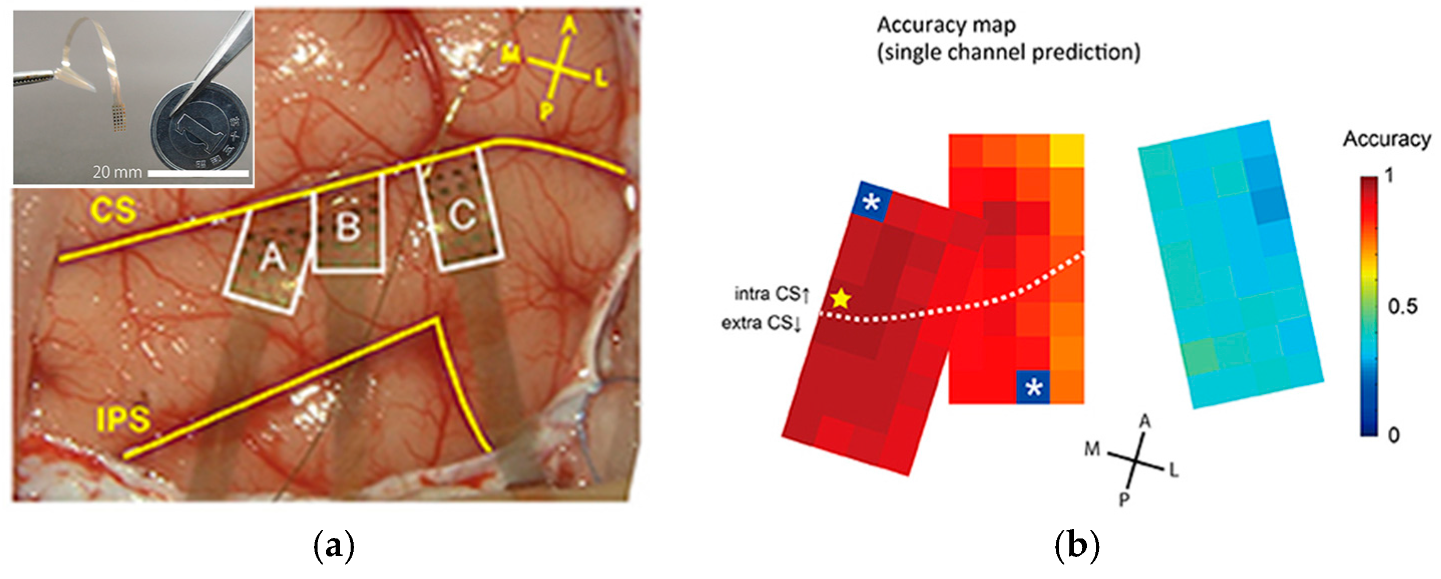
Another recent example was reported by Kaiju et al. that performed somatosensory evoked potentials (SEPs) analysis on macaque monkeys [103]. They made use of three MEAs, each of them counting 32 gold electrodes deposited onto a flexible parylene-C substrate, where a golden wire was used as a reference electrode (Figure 4a). Stimulating the brain activity by means of a coil electrode for finger stimulation, the authors were able to predict (with maximum accuracy reached in less than 15 ms) which finger was stimulated and the intensity of the stimulation (a map of the accuracy is reported in Figure 4b). Their results are comparable to those obtained by multi-unit studies using penetrating electrodes [104,105], promoting the suitability of flexible ECoG electrodes in recording neural activity. Moreover, unlike penetrating electrodes, the position of soft and flexible ECoG arrays can be easily adjusted during surgery without damaging the brain tissues, thus ensuring that the implant perfectly adheres to the curved surface of the brain.
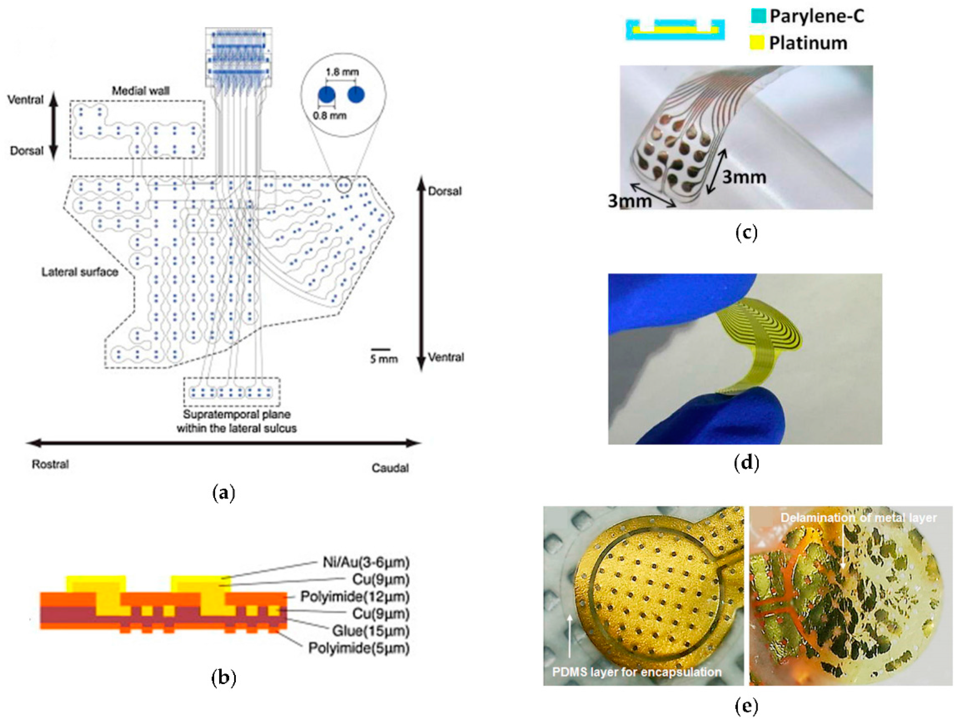
Another important advantage of flexible ECoG electrodes is that the implants fabricated onto organic substrates can be easily fabricated in a lot of different forms and shapes. This is a very interesting and important feature which allows to design electrodes optimized for the recording of specific areas. Thanks to these properties, Fukushima et al. developed an ECoG array consisting in 256 electrodes for bipolar recording at 128 sites (Figure 5a) to record neural activity simultaneously from the medial and lateral cortical surface and from the supratemporal plane (STP) in monkeys [101]. Figure 5b shows a cross section of the MEA used in [101], which consist in a very thin polyimide (PI) substrate with copper electrodes that were insulated by 12-µm thick PI, except for the exposed pad that were plated in gold, hence ensuring the biocompatibility of the implant. Another common organic material used to fabricate flexible substrates and biocompatible encapsulation is parylene-C [106,107,108]. Such highly versatile material features a high purity that reduces the charge trapping phenomena, hence it allows the fabrication of highly stable structures [109]. An example is reported in Figure 5c, where a 16 platinum electrodes (one of which working as reference electrode) array was fabricated onto 12-µm thick flexible parylene-C substrate [110].
Notice that, in order to allow minimal implantation damage and to fit the curved surface of the neuronal tissues, device thickness, flexibility and bio-compatibility are the criteria to design functional ECoG electrodes that allow in vivo recording during behaviour. However, another important criterion is the electrochemical impedance of the implanted electrodes that should be as small as possible. For this reason, Dong et al. fabricated a 32 channel MEAs with Cr/Ag/Cr electrodes (Figure 5d) showing that the less expensive silver electrodes feature a much smaller impedance as respect to standard gold and platinum electrodes [111].
Despite all the advantages with respect to standard electrodes, one major failure mechanism of flexible MEAs is the delamination of the metal electrodes (e.g., gold) on top of the organic substrate. Lee et al. solved this issue by encapsulating the electrodes using polydimethylsiloxane (PDMS) [112]. Figure 5e shows the comparison between gold electrodes with and without PDMS encapsulation. Remarkably, despite the increase of the electrode impedance, the PDMS-coated electrode is still able to correctly detect the biological signals through capacitive coupling with the living tissue while preventing the delamination of the gold electrode.
Instead of using PDMS as a dielectric insulator, a trade-off between low impedance electrodes and long-term stability can be achieved by means of conductive polymers like polypyrrole and poly(3,4-ethylenedioxythiophene) (PEDOT), that are typically doped with poly(styrene sulfonate) (PSS) [113,114]. The organic coatings help to prevent delamination and corrosion of the metal layer that is no-longer in direct contact with the ionic solution. At the same time, the increased roughness of the coated electrodes allows the realization of micro-electrodes with a larger effective area and with the capability of transport both electronic and ionic charges, hence reducing the overall electrodes impedance up to two orders of magnitude with respect to bare gold electrodes.
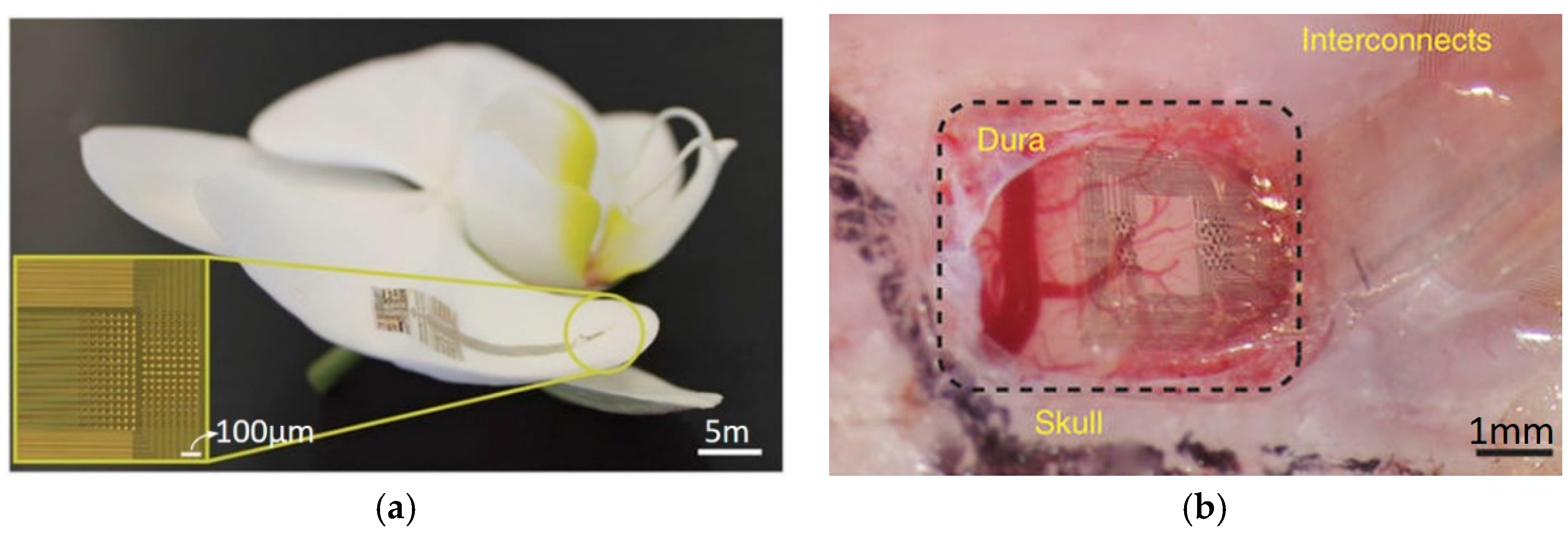
Following this idea, Khodagholy et al. developed an array of 256 PEDOT:PSS electrodes onto a parylene C substrate [115] (Figure 6). Featuring an interelectrode spacing of 30 µm, such flexible and organic ECoG MEA was able to carry out in vivo recording of both local field and action potentials with an excellent implant stability, paving the way to all organic conformable neural interfaces.
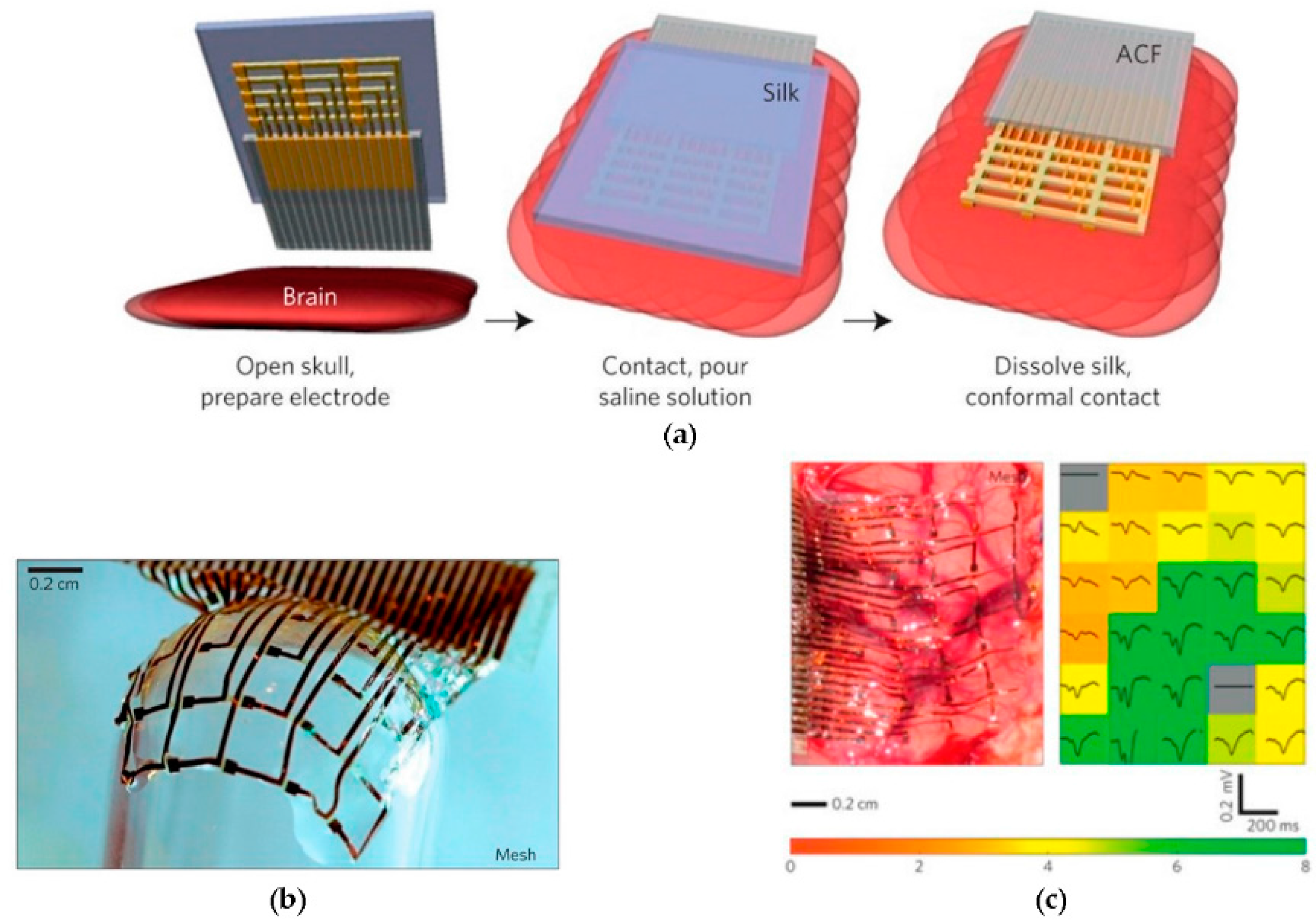
Another outstanding result was achieved by Kim et al. who created a mesh of 30 gold electrodes fabricated on top of a silk bio-resorbable substrate [27]. They first fabricated MEAs on top of PI substrates featuring different thicknesses (from 2.5 µm up to 76 µm), showing that the adhesion between the sensor and the irregular brain surface increases reducing the thickness of the device. Hence, they fabricated a mesh of electrodes onto a silk support that, once applied to the wet surface of the brain, starts to dissolve leaving exposed only the electrodes that get conformally wrapped to the brain surface creating a perfect adhesion (Figure 7). The dissolved silk substrate gets resorbed by the brain tissue.
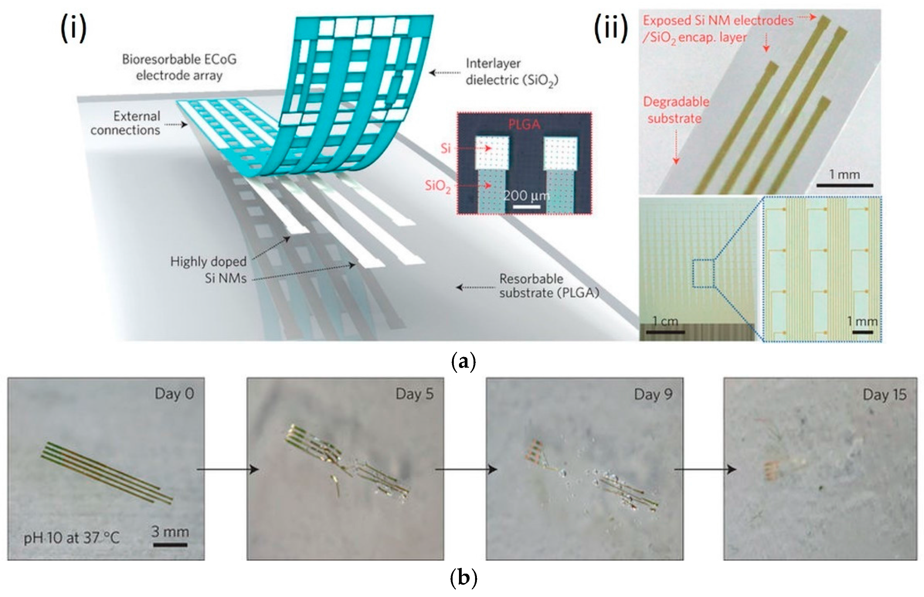
Remarkably, fully resorbable flexible neural interfaces have been recently reported [116,117]. The authors, using standard CMOS technology, fabricated silicon electrodes and transistors that were subsequently transferred onto a dissolvable polymer. Figure 8a shows the structure of the silicon grid, whereas Figure 8b reports an accelerated dissolution test showing the almost complete dissolution of the neural interface. The time for complete dissolution of the device immersed in biofluid at 37 °C has been estimated to be less than two months, hence making such technology suitable for epilepsy patients.
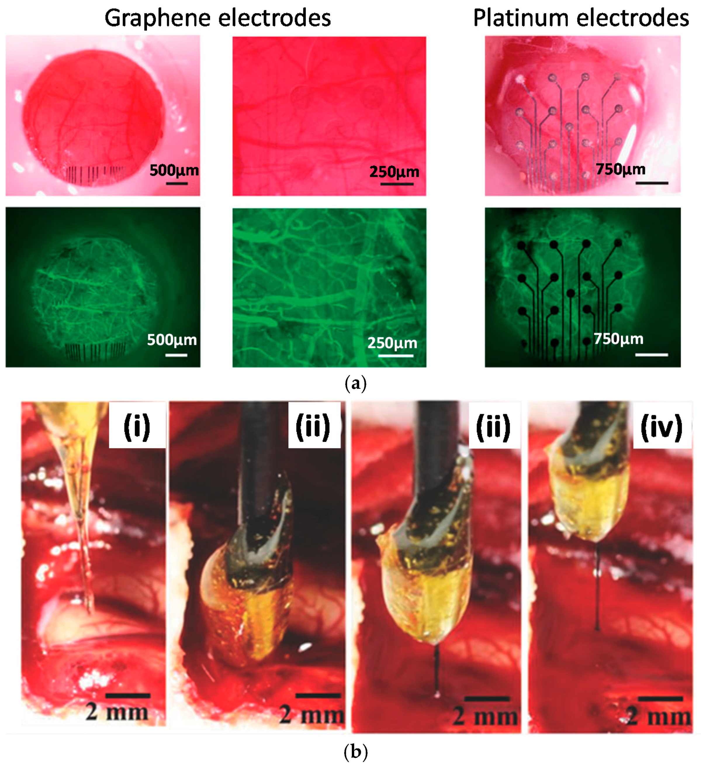
At last, graphene and penetrating electrodes are worth to be mentioned. Graphene electrodes have a slightly higher impedance and smaller charge injection capacity compared to platinum and gold electrodes. However, metal electrodes have a low light transmission, limiting their usefulness in combining electrical recording/stimulation with optical imaging, calcium imaging or optogenetic stimulation of cells [118]. Hence, to overcame this limitation, Park et al. fabricated an array of graphene-based electrodes on top of a parylene-C substrate and they performed bright-field and fluorescence images comparing the results with standard platinum electrodes (Figure 9a) [119].
Aside planar graphene electrodes, carbon nanofiber impregnated into conductive polyethylene [120] and graphene oxide microfibers insulated with parylene-C [121] flexible and penetrating electrodes have been developed. These flexible organic and hybrid electrodes can be introduced deep in the brain through releasable injection microneedles [122] or capillary syringe needles [123], can be stereotaxically implanted after rapid freezing in liquid nitrogen [124] or by coating the electrodes with a rigid and dissolvable sucrose carrier needle [121] (Figure 9b). Such techniques allow the insertion of flexible probes able to perform deep brain stimulations by reducing the risk of tissues damaging after the implant due to motions of the implant itself.
3.2. Organic Field-Effect Transistors
Organic and flexible MEAs have proven to allow reliable in vivo recording by reducing the risk of rejection of the implant as respect to their inorganic counterpart. However, since passive electrodes can provide a limited SNR, organic transistor-based sensors that are able to perform in-situ amplification of the recorded signals are being investigated. Such transistors can be classified in two categories: organic electrochemical transistors (OECTs) and electrolyte-gated organic field-effect transistors (EGOFETs).
OECTs date back to 1984 and polypyrrole was used as conductive polymer [125]. Now, the most commonly used material is PEDOT that can be doped with PSS as well as glycosaminoglycan to enhance its conductivity and/or its biocompatibility [126]. In a OECT, the source-to-drain current is modulated by ions penetrating the polymer hence doping/de-doping the material and consequently modulating the concentration of carriers contributing to the current [127]. Therefore, such interaction between ionic and electronic worlds promote the use of OECTs to realize flexible and biocompatible neural interfaces with high SNR.
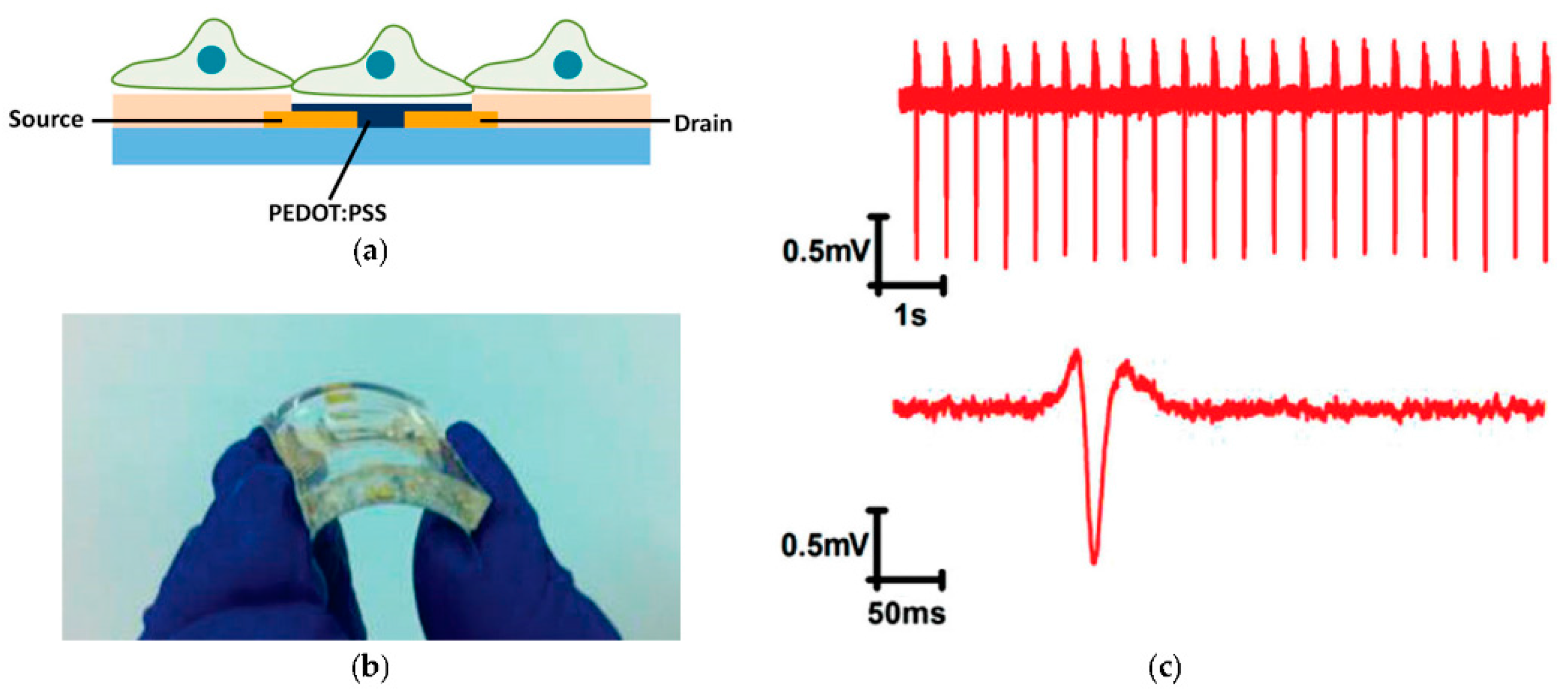
An example was recently reported by Yao et al. who fabricated OECTs sensors on both rigid and flexible substrates (Figure 10a,b), demonstrating SNRs as high as 20 dB during in vitro recording of spontaneously firing cardiomyocyte-like cells (Figure 10b) [128].
Another example was reported by Khodagholy et al. who designed an ECoG probe, where each OECT was juxtapose by a surface electrode, both fabricated using PEDOT:PSS as conductive polymer deposited onto a thin parylene film (Figure 11a) [129]. The authors performed in vivo recording experiments on a rat brain (Figure 11b) and they compare their PEDOT-based sensors with a silicon-base penetrating MEA counting 16 iridium electrodes. The OECT devices were wired in a common source configuration as shown in Figure 11b, with the grounded screw used as the gate electrode. Figure 11c shows the comparison between the three different neural interfaces (OECT, organic surface electrode and inorganic penetrating electrode) simultaneously recording from the same subject and from the same area of the rat brain. Remarkably, the two organic ECoG sensors (OECT and surface electrode) reported higher SNR as respect to the Ir-penetrating electrodes. Moreover, OECT devices yielded to SNRs up to 44 dB, against a 24 dB of simple surface electrodes, highlighting the great advantages of in-situ amplification provided by organic transistors-based neural interfaces.
The same research group realized the architecture reported in [129] over a rigid and removable shuttle, hence fabricating a penetrating and flexible neural interface, where an OECT and an adjacent surface electrode can be inserted deep into the brain [130]. The surface electrode could be used as a local gate for each transistor, as a sink for stimulation currents, or as a simple recording and/or stimulating electrode. Figure 11d shows the penetrating probe (flexible neural interface and shuttle) as well as the representation of how the probe is inserted and how the shuttle is delaminated from the parylene substrate and therefore removed from the brain.
Similarly to OECT technology, electrolyte-gated organic field-effect transistors (EGOFETs)—also known as water-gated OFETs—are worth mentioning. EGOFETs can operate either with pure water or saline solutions as gate medium and they can be fabricated using many different semiconductors (both p- and n-type) [47,131,132,133]. Such transistors are characterized by currents that are much smaller than the OECT counterpart [134,135]. However, in an OECT, the on/off switch is produced by ions transfer from the electrolyte and the semiconductor (doping/de-doping) [136], whereas only capacitive processes occur for EGOFETs, without charge transfer [137]. Consequently, EGOFETs are intrinsically faster and more stable than OECTs [134], hence they can be successfully employed as sensors for different kind of analytes (for a review see [137]).
Cramer et al. deposited a thin film of pentacene, with a thickness of 9 nm, to fabricate EGOFET devices to perform in vitro recording and stimulation (using the liquid gate as stimulating electrode) of neural network activity (Figure 12a) [138]. They showed that murine neural stem cells can be adhered on top of functional devices without the need of an additional layer of cell-adhesive molecules (e.g., PDL) and then differentiated into neuronal networks (Figure 12b). The EGOFET-based sensor exhibited a very good stability under standard cell culture conditions for nine days and, after liquid-gate stimulation, it was able to successfully detect the neural network activity (Figure 12c). The same group recently showed that EGOFETs devices with incorporated gold nanoparticles (Figure 12d) can behave both as a transistor and as a memristor [139], hence opening the door to new multifunctional bio-sensing devices.
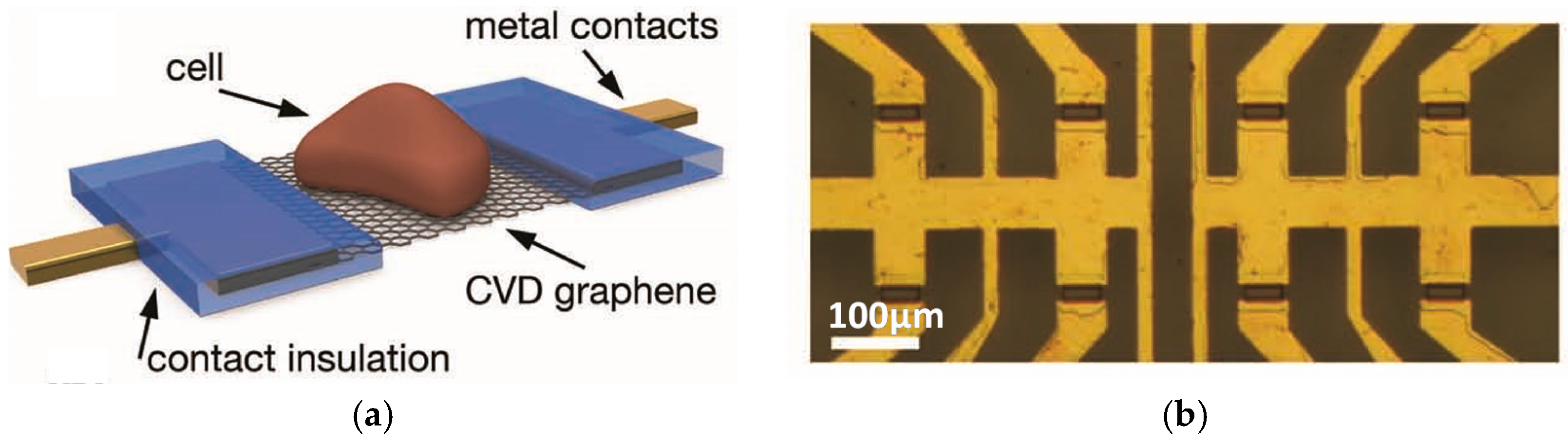
Graphene solution-gated field-effect transistors (G-SGFETs) depicted in Figure 13a, are another alternative to stiff inorganic neural interfaces. Hess et al. fabricated an array of graphene transistors onto a rigid substrate (Figure 13b) and demonstrated that G-SGFETs are capable to record cell signals with SNRs surpassing state-of-the-art devices for bioelectronic applications [140]. Subsequently, the same research group reported the fabrication of flexible arrays of G-SGFETs on polyimide, showing that the electronic properties of their devices do not degrade during repeated bending [141]. After cell culture, they demonstrated that it is possible to perform recording of cell action potentials from cardiomyocyte-like cells with a high SNR. Moreover, in vivo recording of brain activity was recently reported by the same research group [142], proving that graphene-based sensors could pave the way to new high performance neural interfaces for in vivo recording.
Finally, it is important to notice that, each neural interface described so far require the presence of a reference electrode to set the MEA reference potential or to set the operative point of the transistor-based sensor (gate electrode). However, to maximize the suitability for in vivo recording and to overcame the drawback of the presence of an additional and often invasive, electrode, it is highly desirable to avoid the presence of the reference electrode.
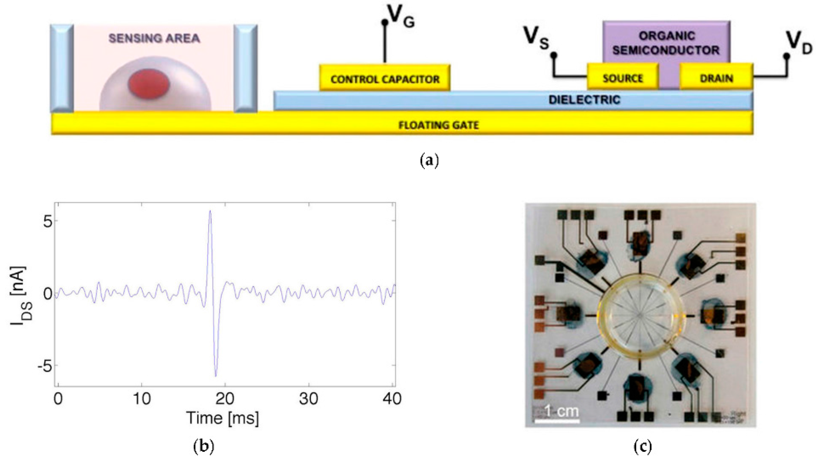
For this reason, Spanu et al. developed a reference-less organic transistor-based sensor called organic charge modulated field-effect transistor (OCMFET) [143]. The OCMFET device depicted in Figure 14a is characterized by a floating gate and a control gate. The latter set the operative point of the transistor, whereas the floating gate, i.e., the OCMFET sensing area, extends outside of the active area of the transistor. Ionic charge variations occurring in proximity of the sensing area determine a charge separation in the floating gate corresponding to a variation of the threshold voltage of the transistor, hence modulating the drain-to-source current. Since the modulation of current is induced only by the variation of ions in the proximity of the floating gate sensing area, cell activity can be successfully recorded without need of any reference electrode (Figure 14b). Remarkably, the OCMFET architecture allows to separate the sensing area from the transducing transistor (Figure 14c), hence the organic transistor can be design and optimized regardless its chemical stability, since it does not need to be in direct contact with any solutions and it can be opportunely encapsulated.
4. Modelling Neural Interfaces
In the previous sections, we reviewed different neural interfaces, focusing our attention to the latest findings in the field of flexible and organic bio-electronics. Now it is important to spend few words about the modelling of such systems and therefore to understand how to interpret the collected data.
Figure 15 shows the simplest equivalent circuit model that can be adapted to describe the interaction between the cell membrane and a micro-electrode (Figure 15a) as well as a generic transistor (Figure 15b). Despite their simplicity, such models are very useful to understand the general working principle of extracellular recording. Indeed, the neuronal activity is given by ionic currents flowing across the cell membrane, changing both the intracellular potential, VM and extracellular potential, VJ. The extracellular potential leads to an electrochemical current at the electrode/electrolyte interface (Figure 15a) or drives the gate of the transistor-base sensor modulating its drain-to-source current (Figure 15b) [40].
Although such simple models can help in the understanding of the bio-sensors working principles, they do not allow an intimate knowledge of the cell activity and how the recorded signals are affected by the interaction between neurons and sensors. This is still a subject of intense investigation that had led to a significant number of publications in the last two decades [144,145,146,147,148,149,150,151,152].
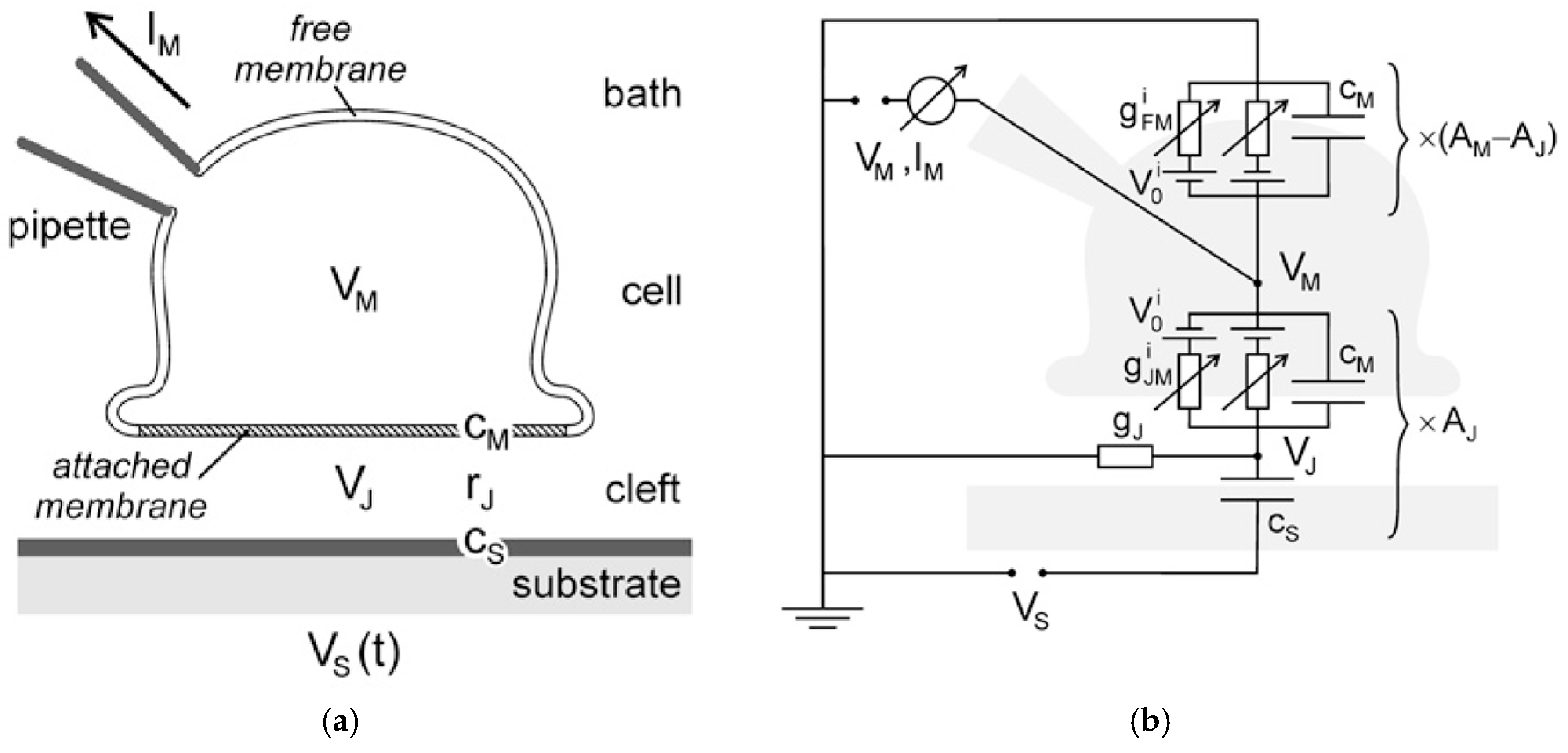
Figure 16 shows the equivalent circuit model for a neuron interfacing a biosensor. Even though such model dates back to the nineties [146], it is a very powerful tool in understanding cells behaviour under current and voltage stimuli as well as in the interpretation of the recorded data both from micro-electrodes and transistors. Moreover, all the different models until now proposed are derived (with suitable modifications) from the model of Figure 16b [147,149,150,151,152].
Using the equivalent circuit of Figure 16b, Fromherz proposed the approximation of a fast (the relaxation of the junction is fast compared with the dynamics of the response), weak (the ionic channels’ conductance are much smaller than the junction conductance gJ) and small (the area of the attached membrane is much smaller than the area of the free membrane) cell-silicon junction to interpret the data recorded by a EOSFET (Figure 17a) [146].
In addition, the model in Figure 16b can be used to rationalize the mechanism behind extracellular stimulations by means of a capacitive electrode [148]. Neuronal excitation is elicited under current-clamp by two mechanisms: (i) falling voltage ramps and pulses depolarize the attached membrane triggering an action potential (Figure 17b); (ii) rising voltage ramps and pulses, instead, depolarize the free membrane, hence an action potential is triggered (Figure 17c).
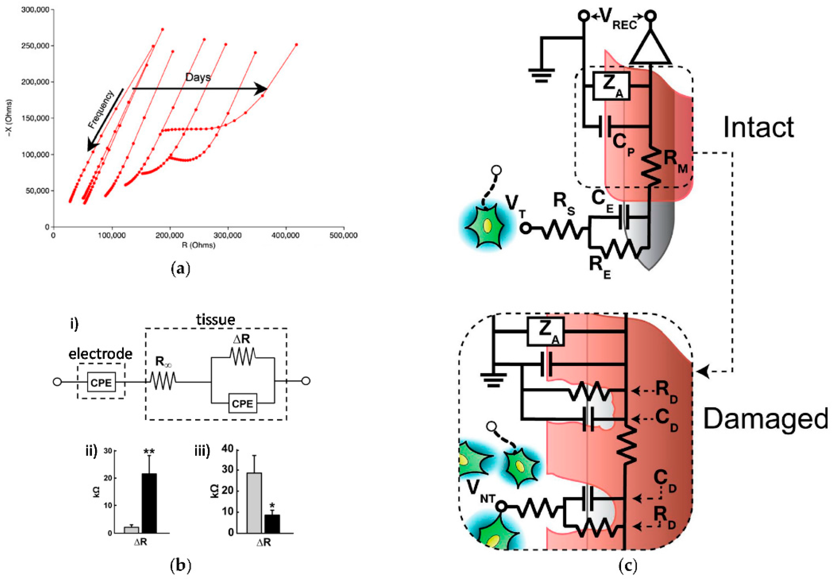
Finally, to underline the importance of equivalent circuit models in investigating the nature of the sensor/electrolyte interface, it is worth to remark that electrochemical impedance spectroscopy (EIS) is a powerful tool that can help to rationalize the different phenomena occurring at the interface between neurons and sensors [153,154,155,156]. Remarkably, opportune equivalent impedance models can be combined with in vivo electrochemical impedance spectroscopy to monitor the state of the implant during time [52,157,158,159,160,161,162]. For instance, Williams et al. performed EIS measurements of implanted electrodes upon implants duration from 7 up to 21 days [52]. Figure 18a reports an example of impedance variation due to an extensive histological reaction that lead to a significant increase of the measured impedance and consequently, to the implant failure.
Another example of using EIS as a tool to characterize the implant during in vivo applications was reported by Lempka et al. [157]. They characterized deep-brain stimulation electrodes using the model in Figure 18b, where they separated the tissue components by the electrode components and they monitor variations in the model parameters after implantations and after a neural stimulation. As previously reported by Williams et al. following the implantation, the electrode impedance increases. Remarkably, the stimulation produces a rapid decrease in electrode impedance with extensive changes in the tissue component promoting the use of voltage pulses to improve the performance of implanted electrodes [57,58].
Similarly, Caldwell et al. performed EIS measurement to investigated the formation of undesired conductive paths and consequent loss of functionality in the implant [162]. By analysing the impedance of the implant, the authors showed that such unwanted paths are due to the damaging of the electrode insulator, as reported in the model of Figure 18c. In fact, a comprehensive model of the metal/organic semiconductor/electrolyte describing the percolation of solution through the organic material has been recently proposed [156].
Hence proving how the combination of EIS measurements and proper models can pave the way to intimately understand and optimize neural interfaces for long term in vivo implants.
5. Conclusions and Future Perspective
The latest achievements in flexible and organic neural interfaces have been reviewed. State-of-the-art inorganic technologies allow both in vivo and in vitro recording of neural activity. However, the rigidity and stiffness of the inorganic materials do not fully meet the biocompatibility requirements needed to achieve long term stability and reliability in vivo. Hence, to promote a good interaction between living tissues and implants, reducing the risk of implant rejection and/or of inflammatory responses, suitable coatings and functionalizations with soft and biocompatible polymers are required.
For these reasons, organic electronics appears to be a valid alternative to conventional technologies, allowing the realization of more flexible and conformable neural interfaces that can be intrinsically biocompatible, since the nature of the organic semiconductors is similar to that of the living tissues as respect with the inorganic counterpart. Moreover, organic materials can be tuned to enhance the device sensitivity to a particular analyte and flexible neural interfaces can be fabricated onto transparent substrate promoting the combination of optical and electrical analysis.
The most attractive technology is that based on organic field-effect transistors (both OECTs and EGOFETs) that allow the integration of sensing and amplification in a single device. Such neural interfaces have proven a SNR higher than inorganic-based sensors, paving the way to new all-organic biosensors for in vivo recording of brain activity with minimum risk of tissues damaging. Furthermore, organic neural interfaces that does not need the presence of an external reference electrode have been recently proposed.
Despite all these achievements, the understanding of the transduction mechanism between cells and transistor-based sensors did not progress as fast as the development of new technologies. Moreover, organic transistors and organic transistor based sensors are a relative novel technology that differs in many aspects from standard silicon transistors. In order to master the transduction mechanism behind an organic neural interface working principle, it is therefore important the development of new tools and techniques to characterize and describe the physics of charge transport in organic transistors, as well to fully understand and to model the interaction between ionic solution and organic semiconductor. Lastly, organic neural interfaces still suffer from a low selectivity due to a reduced integration capability with respect to the CMOS technology.
Therefore, it is important to develop new fabrication processes and new technologies to achieve in vivo single-cell bidirectional communication. In addition, to maximize the suitability for in vivo applications, it is desirable to develop new reference-less neural interfaces that, unlike what so far reported, might be suitable for the fabrication of new ECoG arrays with a high integration of reference-less sensors, each able to simultaneous stimulation and recording of cell activity.
Conflicts of Interest
The authors declare no conflict of interest.
References
- Eley, D.D.; Parfitt, G.D.; Perry, M.J.; Taysum, D.H. The semiconductivity of organic substances. Part 1. Trans. Faraday Soc. 1953, 49, 79–86. [Google Scholar] [CrossRef]
- Akamatu, H.; Inokuchi, H. Photoconductivity of Violanthrone. J. Chem. Phys. 1952, 20, 1481–1483. [Google Scholar] [CrossRef]
- Brophy, J.J. Organic semiconductors. Phys. Today 1961, 14, 40–41. [Google Scholar] [CrossRef]
- McNeill, R.; Siudak, R.; Wardlaw, J.; Weiss, D. Electronic Conduction in Polymers. I. The Chemical Structure of Polypyrrole. Aust. J. Chem. 1963, 16, 1056–1075. [Google Scholar] [CrossRef]
- Bolto, B.; McNeill, R.; Weiss, D. Electronic Conduction in Polymers. III. Electronic Properties of Polypyrrole. Aust. J. Chem. 1963, 16, 1090–1103. [Google Scholar] [CrossRef]
- Berets, D.J.; Smith, D.S. Electrical properties of linear polyacetylene. Trans. Faraday Soc. 1968, 64, 823–828. [Google Scholar] [CrossRef]
- Chiang, C.K.; Fincher, C.R.; Park, Y.W.; Heeger, A.J.; Shirakawa, H.; Louis, E.J.; Gau, S.C.; MacDiarmid, A.G. Electrical Conductivity in Doped Polyacetylene. Phys. Rev. Lett. 1977, 39, 1098–1101. [Google Scholar] [CrossRef]
- Williams, D.F.; Schadt, M. A simple organic electroluminescent diode. Proc. IEEE 1970, 58, 476. [Google Scholar] [CrossRef]
- Tang, C.W.; VanSlyke, S.A. Organic electroluminescent diodes. Appl. Phys. Lett. 1987, 51, 913–915. [Google Scholar] [CrossRef]
- Burroughes, J.H.; Bradley, D.D.C.; Brown, A.R.; Marks, R.N.; Mackay, K.; Friend, R.H.; Burns, P.L.; Holmes, A.B. Light-emitting diodes based on conjugated polymers. Nature 1990, 347, 539–541. [Google Scholar] [CrossRef]
- Tang, C.W. Two-layer organic photovoltaic cell. Appl. Phys. Lett. 1986, 48, 183–185. [Google Scholar] [CrossRef]
- Shin, S.S.; Yeom, E.J.; Yang, W.S.; Hur, S.; Kim, M.G.; Im, J.; Seo, J.; Noh, J.H.; Seok, S.I. Colloidally prepared La-doped BaSnO3 electrodes for efficient, photostable perovskite solar cells. Science 2017, 356, 167–171. [Google Scholar] [CrossRef] [PubMed]
- Garnier, F.; Horowitz, G.; Peng, X.; Fichou, D. An all-organic “soft” thin film transistor with very high carrier mobility. Adv. Mater. 1990, 2, 592–594. [Google Scholar] [CrossRef]
- Hepp, A.; Heil, H.; Weise, W.; Ahles, M.; Schmechel, R.; von Seggern, H. Light-Emitting Field-Effect Transistor Based on a Tetracene Thin Film. Phys. Rev. Lett. 2003, 91, 157406. [Google Scholar] [CrossRef] [PubMed]
- Lin, P.; Yan, F. Organic Thin-Film Transistors for Chemical and Biological Sensing. Adv. Mater. 2012, 24, 34–51. [Google Scholar] [CrossRef] [PubMed]
- An, B.W.; Shin, J.H.; Kim, S.-Y.; Kim, J.; Ji, S.; Park, J.; Lee, Y.; Jang, J.; Park, Y.-G.; Cho, E.; et al. Smart Sensor Systems for Wearable Electronic Devices. Polymers 2017, 9, 303. [Google Scholar] [CrossRef]
- Khan, R.S.; Khurshid, Z.; Yahya Ibrahim Asiri, F. Advancing Point-of-Care (PoC) Testing Using Human Saliva as Liquid Biopsy. Diagnostics 2017, 7, 39. [Google Scholar] [CrossRef] [PubMed]
- Gustafsson, G.; Cao, Y.; Treacy, G.M.; Klavetter, F.; Colaneri, N.; Heeger, A.J. Flexible light-emitting diodes made from soluble conducting polymers. Nature 1992, 357, 477–479. [Google Scholar] [CrossRef]
- Sirringhaus, H.; Kawase, T.; Friend, R.H.; Shimoda, T.; Inbasekaran, M.; Wu, W.; Woo, E.P. High-Resolution Inkjet Printing of All-Polymer Transistor Circuits. Science 2000, 290, 2123–2126. [Google Scholar] [CrossRef] [PubMed]
- Berggren, M.; Richter-Dahlfors, A. Organic Bioelectronics. Adv. Mater. 2007, 19, 3201–3213. [Google Scholar] [CrossRef]
- Khan, M.S.; Misra, S.K.; Wang, Z.; Daza, E.; Schwartz-Duval, A.S.; Kus, J.M.; Pan, D.; Pan, D. Paper-Based Analytical Biosensor Chip Designed from Graphene-Nanoplatelet-Amphiphilic-diblock-co-Polymer Composite for Cortisol Detection in Human Saliva. Anal. Chem. 2017, 89, 2107–2115. [Google Scholar] [CrossRef] [PubMed]
- Khan, M.S.; Misra, S.K.; Schwartz-Duval, A.S.; Daza, E.; Ostadhossein, F.; Bowman, M.; Jain, A.; Taylor, G.; McDonagh, D.; Labriola, L.T.; et al. Real-Time Monitoring of Post-Surgical and Post-Traumatic Eye Injuries Using Multilayered Electrical Biosensor Chip. ACS Appl. Mater. Interfaces 2017, 9, 8609–8622. [Google Scholar] [CrossRef] [PubMed]
- Khan, M.S.; Dosoky, N.S.; Williams, J.D. Engineering Lipid Bilayer Membranes for Protein Studies. Int. J. Mol. Sci. 2013, 14, 21561–21597. [Google Scholar] [CrossRef] [PubMed]
- Khan, M.S.; Dosoky, N.S.; Berdiev, B.K.; Williams, J.D. Electrochemical impedance spectroscopy for black lipid membranes fused with channel protein supported on solid-state nanopore. Eur. Biophys. J. 2016, 45, 843–852. [Google Scholar] [CrossRef] [PubMed]
- Tengvall, P.; Lundström, I.; Liedberg, B. Protein adsorption studies on model organic surfaces: An ellipsometric and infrared spectroscopic approach. Biomaterials 1998, 19, 407–422. [Google Scholar] [CrossRef]
- Głowacki, E.D.; Irimia-Vladu, M.; Kaltenbrunner, M.; Gsiorowski, J.; White, M.S.; Monkowius, U.; Romanazzi, G.; Suranna, G.P.; Mastrorilli, P.; Sekitani, T.; et al. Hydrogen-Bonded Semiconducting Pigments for Air-Stable Field-Effect Transistors. Adv. Mater. 2013, 25, 1563–1569. [Google Scholar] [CrossRef] [PubMed]
- Kim, D.-H.; Viventi, J.; Amsden, J.J.; Xiao, J.; Vigeland, L.; Kim, Y.-S.; Blanco, J.A.; Panilaitis, B.; Frechette, E.S.; Contreras, D.; et al. Dissolvable films of silk fibroin for ultrathin conformal bio-integrated electronics. Nat. Mater. 2010, 9, 511–517. [Google Scholar] [CrossRef] [PubMed]
- Sirringhaus, H. Reliability of Organic Field-Effect Transistors. Adv. Mater. 2009, 21, 3859–3873. [Google Scholar] [CrossRef]
- Klauk, H. Organic thin-film transistors. Chem. Soc. Rev. 2010, 39, 2643–2666. [Google Scholar] [CrossRef] [PubMed]
- Huang, K.-M.; Lin, H.-C.; Kawashima, K.; Osaka, I.; Zan, H.-W.; Meng, H.-F.; Takimiya, K. 2-V operated flexible vertical organic transistor with good air stability and bias stress reliability. Org. Electron. 2017, 50, 325–330. [Google Scholar] [CrossRef]
- Kuribara, K.; Wang, H.; Uchiyama, N.; Fukuda, K.; Yokota, T.; Zschieschang, U.; Jaye, C.; Fischer, D.; Klauk, H.; Yamamoto, T.; et al. Organic transistors with high thermal stability for medical applications. Nat. Commun. 2012, 3, 723. [Google Scholar] [CrossRef] [PubMed]
- Sekitani, T.; Zschieschang, U.; Klauk, H.; Someya, T. Flexible organic transistors and circuits with extreme bending stability. Nat. Mater. 2010, 9, 1015–1022. [Google Scholar] [CrossRef] [PubMed]
- Takeya, J.; Yamagishi, M.; Tominari, Y.; Hirahara, R.; Nakazawa, Y.; Nishikawa, T.; Kawase, T.; Shimoda, T.; Ogawa, S. Very high-mobility organic single-crystal transistors with in-crystal conduction channels. Appl. Phys. Lett. 2007, 90, 102120. [Google Scholar] [CrossRef]
- Kang, I.; Yun, H.-J.; Chung, D.S.; Kwon, S.-K.; Kim, Y.-H. Record High Hole Mobility in Polymer Semiconductors via Side-Chain Engineering. J. Am. Chem. Soc. 2013, 135, 14896–14899. [Google Scholar] [CrossRef] [PubMed]
- Sun, B.; Hong, W.; Yan, Z.; Aziz, H.; Li, Y. Record High Electron Mobility of 6.3 cm2 V−1 s−1 Achieved for Polymer Semiconductors Using a New Building Block. Adv. Mater. 2014, 26, 2636–2642. [Google Scholar] [CrossRef] [PubMed]
- Wang, L.; Zhang, X.; Dai, G.; Deng, W.; Jie, J.; Zhang, X. High-mobility air-stable n-type field-effect transistors based on large-area solution-processed organic single-crystal arrays. Nano Res. 2017. [Google Scholar] [CrossRef]
- Buzsáki, G.; Anastassiou, C.A.; Koch, C. The origin of extracellular fields and currents—EEG, ECoG, LFP and spikes. Nat. Rev. Neurosci. 2012, 13, 407–420. [Google Scholar] [CrossRef] [PubMed]
- Peyron, R.; Laurent, B.; García-Larrea, L. Functional imaging of brain responses to pain. A review and meta-analysis (2000). Neurophysiol. Clin. Neurophysiol. 2000, 30, 263–288. [Google Scholar] [CrossRef]
- Menon, V.; Ford, J.M.; Lim, K.O.; Glover, G.H.; Pfefferbaum, A. Combined event-related fMRI and EEG evidence for temporal—Parietal cortex activation during target detection. NeuroReport 1997, 8, 3029–3037. [Google Scholar] [CrossRef] [PubMed]
- Fang, Y.; Li, X.; Fang, Y. Organic bioelectronics for neural interfaces. J. Mater. Chem. C 2015, 3, 6424–6430. [Google Scholar] [CrossRef]
- Alivisatos, A.P.; Andrews, A.M.; Boyden, E.S.; Chun, M.; Church, G.M.; Deisseroth, K.; Donoghue, J.P.; Fraser, S.E.; Lippincott-Schwartz, J.; Looger, L.L.; et al. Nanotools for Neuroscience and Brain Activity Mapping. ACS Nano 2013, 7, 1850–1866. [Google Scholar] [CrossRef] [PubMed]
- Fattahi, P.; Yang, G.; Kim, G.; Abidian, M.R. A Review of Organic and Inorganic Biomaterials for Neural Interfaces. Adv. Mater. 2014, 26, 1846–1885. [Google Scholar] [CrossRef] [PubMed]
- Torsi, L.; Magliulo, M.; Manoli, K.; Palazzo, G. Organic field-effect transistor sensors: A tutorial review. Chem. Soc. Rev. 2013, 42, 8612–8628. [Google Scholar] [CrossRef] [PubMed]
- Kotov, N.A.; Winter, J.O.; Clements, I.P.; Jan, E.; Timko, B.P.; Campidelli, S.; Pathak, S.; Mazzatenta, A.; Lieber, C.M.; Prato, M.; et al. Nanomaterials for Neural Interfaces. Adv. Mater. 2009, 21, 3970–4004. [Google Scholar] [CrossRef]
- Chen, R.; Canales, A.; Anikeeva, P. Neural recording and modulation technologies. Nat. Rev. Mater. 2017, 2, 16093. [Google Scholar] [CrossRef]
- Deslouis, C.; Moustafid, T.E.; Musiani, M.M.; Tribollet, B. Mixed ionic-electronic conduction of a conducting polymer film. Ac impedance study of polypyrrole. Electrochim. Acta 1996, 41, 1343–1349. [Google Scholar] [CrossRef]
- Porrazzo, R.; Bellani, S.; Luzio, A.; Lanzarini, E.; Caironi, M.; Antognazza, M.R. Improving mobility and electrochemical stability of a water-gated polymer field-effect transistor. Org. Electron. 2014, 15, 2126–2134. [Google Scholar] [CrossRef]
- Negi, S.; Bhandari, R.; Rieth, L.; Wagenen, R.V.; Solzbacher, F. Neural electrode degradation from continuous electrical stimulation: Comparison of sputtered and activated iridium oxide. J. Neurosci. Methods 2010, 186, 8–17. [Google Scholar] [CrossRef] [PubMed]
- Polikov, V.S.; Tresco, P.A.; Reichert, W.M. Response of brain tissue to chronically implanted neural electrodes. J. Neurosci. Methods 2005, 148, 1–18. [Google Scholar] [CrossRef] [PubMed]
- Heiduschka, P.; Thanos, S. Implantable bioelectronic interfaces for lost nerve functions. Prog. Neurobiol. 1998, 55, 433–461. [Google Scholar] [CrossRef]
- Edell, D.J.; Toi, V.V.; McNeil, V.M.; Clark, L.D. Factors influencing the biocompatibility of insertable silicon microshafts in cerebral cortex. IEEE Trans. Biomed. Eng. 1992, 39, 635–643. [Google Scholar] [CrossRef] [PubMed]
- Williams, J.C.; Hippensteel, J.A.; Dilgen, J.; Shain, W.; Kipke, D.R. Complex impedance spectroscopy for monitoring tissue responses to inserted neural implants. J. Neural Eng. 2007, 4, 410–423. [Google Scholar] [CrossRef] [PubMed]
- McLaughlin, B.L.; Kampasi, K.; Perlin, G.E.; LeBlanc, J.; Achyuta, A.K.H.; Kumar, P.; Cook, G.; Segura, C.; Mittal, V.; Kipke, D. Bi-directional Optrode for quantitative prediction of neural interface failure. In Proceedings of the 2013 6th International IEEE/EMBS Conference on Neural Engineering (NER), San Diego, CA, USA, 6–8 November 2013; pp. 915–918. [Google Scholar]
- Moxon, K.A.; Hallman, S.; Aslani, A.; Kalkhoran, N.M.; Lelkes, P.I. Bioactive properties of nanostructured porous silicon for enhancing electrode to neuron interfaces. J. Biomater. Sci. Polym. Ed. 2007, 18, 1263–1281. [Google Scholar] [CrossRef] [PubMed]
- Szarowski, D.H.; Andersen, M.D.; Retterer, S.; Spence, A.J.; Isaacson, M.; Craighead, H.G.; Turner, J.N.; Shain, W. Brain responses to micro-machined silicon devices. Brain Res. 2003, 983, 23–35. [Google Scholar] [CrossRef]
- Rousche, P.J.; Pellinen, D.S.; Pivin, D.P.; Williams, J.C.; Vetter, R.J.; Kipke, D.R. Flexible polyimide-based intracortical electrode arrays with bioactive capability. IEEE Trans. Biomed. Eng. 2001, 48, 361–371. [Google Scholar] [CrossRef] [PubMed]
- Johnson, M.D.; Otto, K.J.; Kipke, D.R. Repeated voltage biasing improves unit recordings by reducing resistive tissue impedances. IEEE Trans. Neural Syst. Rehabil. Eng. 2005, 13, 160–165. [Google Scholar] [CrossRef] [PubMed]
- Otto, K.J.; Johnson, M.D.; Kipke, D.R. Voltage pulses change neural interface properties and improve unit recordings with chronically implanted microelectrodes. IEEE Trans. Biomed. Eng. 2006, 53, 333–340. [Google Scholar] [CrossRef] [PubMed]
- Khan, S.P.; Auner, G.G.; Newaz, G.M. Influence of nanoscale surface roughness on neural cell attachment on silicon. Nanomed. Nanotechnol. Biol. Med. 2005, 1, 125–129. [Google Scholar] [CrossRef] [PubMed]
- Yang, F.; Xu, C.Y.; Kotaki, M.; Wang, S.; Ramakrishna, S. Characterization of neural stem cells on electrospun poly(l-lactic acid) nanofibrous scaffold. J. Biomater. Sci. Polym. Ed. 2004, 15, 1483–1497. [Google Scholar] [CrossRef] [PubMed]
- Kim, Y.H.; Baek, N.S.; Han, Y.H.; Chung, M.-A.; Jung, S.-D. Enhancement of neuronal cell adhesion by covalent binding of poly-d-lysine. J. Neurosci. Methods 2011, 202, 38–44. [Google Scholar] [CrossRef] [PubMed]
- Piskin, E. Plasma processing of biomaterials. J. Biomater. Sci. Polym. Ed. 1993, 4, 45–60. [Google Scholar] [CrossRef]
- Kishida, A.; Iwata, H.; Tamada, Y.; Ikada, Y. Cell behaviour on polymer surfaces grafted with non-ionic and ionic monomers. Biomaterials 1991, 12, 786–792. [Google Scholar] [CrossRef]
- Arshady, R. Microspheres for biomedical applications: Preparation of reactive and labelled microspheres. Biomaterials 1993, 14, 5–15. [Google Scholar] [CrossRef]
- Amiji, M.; Park, K. Surface modification of polymeric biomaterials with poly(ethylene oxide), albumin and heparin for reduced thrombogenicity. J. Biomater. Sci. Polym. Ed. 1993, 4, 217–234. [Google Scholar] [CrossRef] [PubMed]
- Guidoin, R.; Marceau, D.; Couture, J.; Rao, T.J.; Merhi, Y.; Roy, P.-E.; Faye, D.D. la Collagen coatings as biological sealants for textile arterial prostheses. Biomaterials 1989, 10, 156–165. [Google Scholar] [CrossRef]
- Marois, Y.; Chakfé, N.; Guidoin, R.; Duhamel, R.C.; Roy, R.; Marois, M.; King, M.W.; Douville, Y. An albumin-coated polyester arterial graft: In vivo assessment of biocompatibility and healing characteristics. Biomaterials 1996, 17, 3–14. [Google Scholar] [CrossRef]
- Marois, Y.; Chakfé, N.; Deng, X.; Marois, M.; How, T.; King, M.W.; Guidoin, R. Carbodiimide cross-linked gelatin: A new coating for porous polyester arterial prostheses. Biomaterials 1995, 16, 1131–1139. [Google Scholar] [CrossRef]
- Widge, A.S.; Jeffries-El, M.; Cui, X.; Lagenaur, C.F.; Matsuoka, Y. Self-assembled monolayers of polythiophene conductive polymers improve biocompatibility and electrical impedance of neural electrodes. Biosens. Bioelectron. 2007, 22, 1723–1732. [Google Scholar] [CrossRef] [PubMed]
- Muzzio, N.E.; Pasquale, M.A.; Moya, S.E.; Azzaroni, O. Tailored polyelectrolyte thin film multilayers to modulate cell adhesion. Biointerphases 2017, 12, 04E403. [Google Scholar] [CrossRef] [PubMed]
- Kleinman, H.K.; Cannon, F.B.; Laurie, G.W.; Hassell, J.R.; Aumailley, M.; Terranova, V.P.; Martin, G.R.; DuBois-Dalcq, M. Biological activities of laminin. J. Cell. Biochem. 1985, 27, 317–325. [Google Scholar] [CrossRef] [PubMed]
- Matsuzawa, M.; Liesi, P.; Knoll, W. Chemically modifying glass surfaces to study substratum-guided neurite outgrowth in culture. J. Neurosci. Methods 1996, 69, 189–196. [Google Scholar] [CrossRef]
- Offenhäusser, A.; Sprössler, C.; Matsuzawa, M.; Knoll, W. Electrophysiological development of embryonic hippocampal neurons from the rat grown on synthetic thin films. Neurosci. Lett. 1997, 223, 9–12. [Google Scholar] [CrossRef]
- Joo, S.; Yeon Kim, J.; Lee, E.; Hong, N.; Sun, W.; Nam, Y. Effects of ECM protein micropatterns on the migration and differentiation of adult neural stem cells. Sci. Rep. 2015, 5, 13043. [Google Scholar] [CrossRef] [PubMed]
- White, K.M.R.; Sabatino, J.A.; He, M.; Davis, N.; Tang, N.; Bearer, C.F. Toluene disruption of the functions of L1 cell adhesion molecule at concentrations associated with occupational exposures. Pediatr. Res. 2016, 80, 145–150. [Google Scholar] [CrossRef] [PubMed]
- Tam, W.Y.; Au, N.P.B.; Ma, C.H.E. The association between laminin and microglial morphology in vitro. Sci. Rep. 2016, 6, 28580. [Google Scholar] [CrossRef] [PubMed]
- Suzuki, Y.; Tanihara, M.; Ohnishi, K.; Suzuki, K.; Endo, K.; Nishimura, Y. Cat peripheral nerve regeneration across 50 mm gap repaired with a novel nerve guide composed of freeze-dried alginate gel. Neurosci. Lett. 1999, 259, 75–78. [Google Scholar] [CrossRef]
- Cheng, C.-Y.; Yao, C.-H.; Liu, B.-S.; Liu, C.-J.; Chen, G.-W.; Chen, Y.-S. The role of astragaloside in regeneration of the peripheral nerve system. J. Biomed. Mater. Res. A 2006, 76A, 463–469. [Google Scholar] [CrossRef] [PubMed]
- Goulart, C.O.; Lopes, F.R.P.; Monte, Z.O.; Dantas, S.V.; Souto, A.; Oliveira, J.T.; Almeida, F.M.; Tonda-Turo, C.; Pereira, C.C.; Borges, C.P.; et al. Evaluation of biodegradable polymer conduits—Poly(l-lactic acid)—For guiding sciatic nerve regeneration in mice. Methods 2016, 99, 28–36. [Google Scholar] [CrossRef] [PubMed]
- Capeletti, L.B.; Cardoso, M.B.; dos Santos, J.H.Z.; He, W. Hybrid Thin Film Organosilica Sol–Gel Coatings to Support Neuronal Growth and Limit Astrocyte Growth. ACS Appl. Mater. Interfaces 2016, 8, 27553–27563. [Google Scholar] [CrossRef] [PubMed]
- Harnack, D.; Winter, C.; Meissner, W.; Reum, T.; Kupsch, A.; Morgenstern, R. The effects of electrode material, charge density and stimulation duration on the safety of high-frequency stimulation of the subthalamic nucleus in rats. J. Neurosci. Methods 2004, 138, 207–216. [Google Scholar] [CrossRef] [PubMed]
- Merrill, D.R.; Bikson, M.; Jefferys, J.G.R. Electrical stimulation of excitable tissue: Design of efficacious and safe protocols. J. Neurosci. Methods 2005, 141, 171–198. [Google Scholar] [CrossRef] [PubMed]
- Cogan, S.F.; Guzelian, A.A.; Agnew, W.F.; Yuen, T.G.H.; McCreery, D.B. Over-pulsing degrades activated iridium oxide films used for intracortical neural stimulation. J. Neurosci. Methods 2004, 137, 141–150. [Google Scholar] [CrossRef] [PubMed]
- Twardoch, U.M. Integrity of ultramicro-stimulation electrodes determined from electrochemical measurements. J. Appl. Electrochem. 1994, 24, 835–857. [Google Scholar] [CrossRef]
- Chestek, C.A.; Gilja, V.; Nuyujukian, P.; Foster, J.D.; Fan, J.M.; Kaufman, M.T.; Churchland, M.M.; Rivera-Alvidrez, Z.; Cunningham, J.P.; Ryu, S.I.; et al. Long-term stability of neural prosthetic control signals from silicon cortical arrays in rhesus macaque motor cortex. J. Neural Eng. 2011, 8, 045005. [Google Scholar] [CrossRef] [PubMed]
- Someya, T.; Kato, Y.; Sekitani, T.; Iba, S.; Noguchi, Y.; Murase, Y.; Kawaguchi, H.; Sakurai, T. Conformable, flexible, large-area networks of pressure and thermal sensors with organic transistor active matrixes. Proc. Natl. Acad. Sci. USA 2005, 102, 12321–12325. [Google Scholar] [CrossRef] [PubMed]
- Shiraishi, A.; Uno, T.; Oka, N.; Hara, Y.; Yamaguchi, M.; Ohashi, Y. In Vivo and In Vitro Laser Confocal Microscopy to Diagnose Acanthamoeba Keratitis. Cornea 2010, 29. [Google Scholar] [CrossRef] [PubMed]
- Kapnisis, K.K.; Pitsillides, C.M.; Prokopi, M.S.; Lapathitis, G.; Karaiskos, C.; Eleftheriou, P.C.; Brott, B.C.; Anderson, P.G.; Lemons, J.E.; Anayiotos, A.S. In vivo monitoring of the inflammatory response in a stented mouse aorta model. J. Biomed. Mater. Res. A 2016, 104, 227–238. [Google Scholar] [CrossRef] [PubMed]
- Suter, D.M. Live cell imaging of neuronal growth cone motility and guidance in vitro. Methods Mol. Biol. 2011, 769, 65–86. [Google Scholar] [CrossRef] [PubMed]
- Chen, Z.; Lee, H.; Henle, S.J.; Cheever, T.R.; Ekker, S.C.; Henley, J.R. Primary Neuron Culture for Nerve Growth and Axon Guidance Studies in Zebrafish (Danio rerio). PLoS ONE 2013, 8, e57539. [Google Scholar] [CrossRef] [PubMed]
- Wiegert, J.S.; Gee, C.E.; Oertner, T.G. Stimulating Neurons with Heterologously Expressed Light-Gated Ion Channels. Cold Spring Harb. Protoc. 2017, 2017, pdb.top089714. [Google Scholar] [CrossRef] [PubMed]
- Badi, A.N.; Kertesz, T.R.; Gurgel, R.K.; Shelton, C.; Normann, R.A. Development of a Novel Eighth-Nerve Intraneural Auditory Neuroprosthesis. Laryngoscope 2003, 113, 833–842. [Google Scholar] [CrossRef] [PubMed]
- Barz, F.; Livi, A.; Lanzilotto, M.; Maranesi, M.; Bonini, L.; Paul, O.; Ruther, P. Versatile, modular 3D microelectrode arrays for neuronal ensemble recordings: From design to fabrication, assembly and functional validation in non-human primates. J. Neural Eng. 2017, 14, 036010. [Google Scholar] [CrossRef] [PubMed]
- Eversmann, B.; Jenkner, M.; Hofmann, F.; Paulus, C.; Brederlow, R.; Holzapfl, B.; Fromherz, P.; Merz, M.; Brenner, M.; Schreiter, M.; et al. A 128 × 128 CMOS biosensor array for extracellular recording of neural activity. IEEE J. Solid-State Circuits 2003, 38, 2306–2317. [Google Scholar] [CrossRef]
- Thewes, R.; Bertotti, G.; Dodel, N.; Keil, S.; Schröder, S.; Boven, K.H.; Zeck, G.; Mahmud, M.; Vassanelli, S. Neural tissue and brain interfacing CMOS devices—An introduction to state-of-the-art, current and future challenges. In Proceedings of the 2016 IEEE International Symposium on Circuits and Systems (ISCAS), Montreal, QC, Canada, 22–25 May 2016; pp. 1826–1829. [Google Scholar]
- Poghossian, A.; Ingebrandt, S.; Offenhäusser, A.; Schöning, M.J. Field-effect devices for detecting cellular signals. Semin. Cell. Dev. Biol. 2009, 20, 41–48. [Google Scholar] [CrossRef] [PubMed]
- Felderer, F.; Fromherz, P. Transistor needle chip for recording in brain tissue. Appl. Phys. A 2011, 104, 1. [Google Scholar] [CrossRef]
- Vassanelli, S. Multielectrode and Multitransistor Arrays for In Vivo Recording. In Nanotechnology and Neuroscience: Nano-Electronic, Photonic and Mechanical Neuronal Interfacing; De Vittorio, M., Martiradonna, L., Assad, J., Eds.; Springer: New York, NY, USA, 2014; pp. 239–267. ISBN 978-1-4899-8038-0. [Google Scholar]
- Pistohl, T.; Ball, T.; Schulze-Bonhage, A.; Aertsen, A.; Mehring, C. Prediction of arm movement trajectories from ECoG-recordings in humans. J. Neurosci. Methods 2008, 167, 105–114. [Google Scholar] [CrossRef] [PubMed]
- Nicolelis, M.A.L.; Dimitrov, D.; Carmena, J.M.; Crist, R.; Lehew, G.; Kralik, J.D.; Wise, S.P. Chronic, multisite, multielectrode recordings in macaque monkeys. Proc. Natl. Acad. Sci. USA 2003, 100, 11041–11046. [Google Scholar] [CrossRef] [PubMed]
- Fukushima, M.; Saunders, R.C.; Mullarkey, M.; Doyle, A.M.; Mishkin, M.; Fujii, N. An electrocorticographic electrode array for simultaneous recording from medial, lateral and intrasulcal surface of the cortex in macaque monkeys. J. Neurosci. Methods 2014, 233, 155–165. [Google Scholar] [CrossRef] [PubMed]
- Ahmadi, E.; Katnani, H.A.; Besheli, L.D.; Gu, Q.; Atefi, R.; Villeneuve, M.Y.; Eskandar, E.; Lev, M.H.; Golby, A.J.; Gupta, R.; et al. An Electrocorticography Grid with Conductive Nanoparticles in a Polymer Thick Film on an Organic Substrate Improves CT and MR Imaging. Radiology 2016, 280, 595–601. [Google Scholar] [CrossRef] [PubMed]
- Kaiju, T.; Doi, K.; Yokota, M.; Watanabe, K.; Inoue, M.; Ando, H.; Takahashi, K.; Yoshida, F.; Hirata, M.; Suzuki, T. High Spatiotemporal Resolution ECoG Recording of Somatosensory Evoked Potentials with Flexible Micro-Electrode Arrays. Front. Neural Circuits 2017, 11, 20. [Google Scholar] [CrossRef] [PubMed]
- Nelson, R.J.; Sur, M.; Felleman, D.J.; Kaas, J.H. Representations of the body surface in postcentral parietal cortex of Macaca fascicularis. J. Comp. Neurol. 1980, 192, 611–643. [Google Scholar] [CrossRef] [PubMed]
- Pons, T.P.; Wall, J.T.; Garraghty, P.E.; Cusick, C.G.; Kaas, J.H. Consistent Features of the Representation of the Hand in Area 3b of Macaque Monkeys. Somatosens. Res. 1987, 4, 309–331. [Google Scholar] [CrossRef] [PubMed]
- Takeuchi, S.; Ziegler, D.; Yoshida, Y.; Mabuchi, K.; Suzuki, T. Parylene flexible neural probes integrated with microfluidic channels. Lab Chip 2005, 5, 519–523. [Google Scholar] [CrossRef] [PubMed]
- Seymour, J.P.; Kipke, D.R. Neural probe design for reduced tissue encapsulation in CNS. Biomaterials 2007, 28, 3594–3607. [Google Scholar] [CrossRef] [PubMed]
- Chang, T.Y.; Yadav, V.G.; De Leo, S.; Mohedas, A.; Rajalingam, B.; Chen, C.-L.; Selvarasah, S.; Dokmeci, M.R.; Khademhosseini, A. Cell and Protein Compatibility of Parylene-C Surfaces. Langmuir 2007, 23, 11718–11725. [Google Scholar] [CrossRef] [PubMed]
- Marszalek, T.; Gazicki-Lipman, M.; Ulanski, J. Parylene C as a versatile dielectric material for organic field-effect transistors. Beilstein J. Nanotechnol. 2017, 8, 1532–1545. [Google Scholar] [CrossRef] [PubMed]
- Chang, C.-W.; Chiou, J.-C. A Wireless and Batteryless Microsystem with Implantable Grid Electrode/3-Dimensional Probe Array for ECoG and Extracellular Neural Recording in Rats. Sensors 2013, 13, 4624–4639. [Google Scholar] [CrossRef] [PubMed]
- Dong, S.; Chen, W.; Wang, X.; Zhang, S.; Xu, K.; Zheng, X. Flexible ECoG electrode for implantation and neural signal recording applications. Vacuum 2017, 140, 96–100. [Google Scholar] [CrossRef]
- Lee, S.M.; Byeon, H.J.; Kim, B.H.; Lee, J.; Jeong, J.Y.; Lee, J.H.; Moon, J.-H.; Park, C.; Choi, H.; Lee, S.-H.; et al. Flexible and implantable capacitive microelectrode for bio-potential acquisition. BioChip J. 2017, 11, 153–163. [Google Scholar] [CrossRef]
- Cui, X.; Hetke, J.F.; Wiler, J.A.; Anderson, D.J.; Martin, D.C. Electrochemical deposition and characterization of conducting polymer polypyrrole/PSS on multichannel neural probes. Sens. Actuators Phys. 2001, 93, 8–18. [Google Scholar] [CrossRef]
- Cui, X.; Martin, D.C. Electrochemical deposition and characterization of poly(3,4-ethylenedioxythiophene) on neural microelectrode arrays. Sens. Actuators B Chem. 2003, 89, 92–102. [Google Scholar] [CrossRef]
- Khodagholy, D.; Gelinas, J.N.; Thesen, T.; Doyle, W.; Devinsky, O.; Malliaras, G.G.; Buzsáki, G. NeuroGrid: Recording action potentials from the surface of the brain. Nat. Neurosci. 2014, 18, 310–315. [Google Scholar] [CrossRef] [PubMed]
- Yu, K.J.; Kuzum, D.; Hwang, S.-W.; Kim, B.H.; Juul, H.; Kim, N.H.; Won, S.M.; Chiang, K.; Trumpis, M.; Richardson, A.G.; et al. Bioresorbable silicon electronics for transient spatiotemporal mapping of electrical activity from the cerebral cortex. Nat. Mater. 2016, 15, 782–791. [Google Scholar] [CrossRef] [PubMed]
- Fang, H.; Zhao, J.; Yu, K.J.; Song, E.; Farimani, A.B.; Chiang, C.-H.; Jin, X.; Xue, Y.; Xu, D.; Du, W.; et al. Ultrathin, transferred layers of thermally grown silicon dioxide as biofluid barriers for biointegrated flexible electronic systems. Proc. Natl. Acad. Sci. USA 2016, 113, 11682–11687. [Google Scholar] [CrossRef] [PubMed]
- Harris, A.R.; Wallace, G.G. Organic Electrodes and Communications with Excitable Cells. Adv. Funct. Mater. 2017. [Google Scholar] [CrossRef]
- Park, D.-W.; Schendel, A.A.; Mikael, S.; Brodnick, S.K.; Richner, T.J.; Ness, J.P.; Hayat, M.R.; Atry, F.; Frye, S.T.; Pashaie, R.; et al. Graphene-based carbon-layered electrode array technology for neural imaging and optogenetic applications. Nat. Commun. 2014, 5, 5258. [Google Scholar] [CrossRef] [PubMed]
- Guo, Y.; Jiang, S.; Grena, B.J.B.; Kimbrough, I.F.; Thompson, E.G.; Fink, Y.; Sontheimer, H.; Yoshinobu, T.; Jia, X. Polymer Composite with Carbon Nanofibers Aligned during Thermal Drawing as a Microelectrode for Chronic Neural Interfaces. ACS Nano 2017, 11, 6574–6585. [Google Scholar] [CrossRef] [PubMed]
- Apollo, N.V.; Maturana, M.I.; Tong, W.; Nayagam, D.A.X.; Shivdasani, M.N.; Foroughi, J.; Wallace, G.G.; Prawer, S.; Ibbotson, M.R.; Garrett, D.J. Soft, Flexible Freestanding Neural Stimulation and Recording Electrodes Fabricated from Reduced Graphene Oxide. Adv. Funct. Mater. 2015, 25, 3551–3559. [Google Scholar] [CrossRef]
- Kim, T.; McCall, J.G.; Jung, Y.H.; Huang, X.; Siuda, E.R.; Li, Y.; Song, J.; Song, Y.M.; Pao, H.A.; Kim, R.-H.; et al. Injectable, Cellular-Scale Optoelectronics with Applications for Wireless Optogenetics. Science 2013, 340, 211–216. [Google Scholar] [CrossRef] [PubMed]
- Liu, J.; Fu, T.-M.; Cheng, Z.; Hong, G.; Zhou, T.; Jin, L.; Duvvuri, M.; Jiang, Z.; Kruskal, P.; Xie, C.; et al. Syringe-injectable electronics. Nat. Nano 2015, 10, 629–636. [Google Scholar] [CrossRef] [PubMed]
- Xie, C.; Liu, J.; Fu, T.-M.; Dai, X.; Zhou, W.; Lieber, C.M. Three-dimensional macroporous nanoelectronic networks as minimally invasive brain probes. Nat. Mater. 2015, 14, 1286–1292. [Google Scholar] [CrossRef] [PubMed]
- White, H.S.; Kittlesen, G.P.; Wrighton, M.S. Chemical derivatization of an array of three gold microelectrodes with polypyrrole: Fabrication of a molecule-based transistor. J. Am. Chem. Soc. 1984, 106, 5375–5377. [Google Scholar] [CrossRef]
- Mantione, D.; del Agua, I.; Schaafsma, W.; Diez-Garcia, J.; Castro, B.; Sardon, H.; Mecerreyes, D. Poly(3,4-ethylenedioxythiophene):GlycosAminoGlycan Aqueous Dispersions: Toward Electrically Conductive Bioactive Materials for Neural Interfaces. Macromol. Biosci. 2016, 16, 1227–1238. [Google Scholar] [CrossRef] [PubMed]
- Bernards, D.A.; Malliaras, G.G. Steady-State and Transient Behavior of Organic Electrochemical Transistors. Adv. Funct. Mater. 2007, 17, 3538–3544. [Google Scholar] [CrossRef]
- Yao, C.; Li, Q.; Guo, J.; Yan, F.; Hsing, I.-M. Rigid and Flexible Organic Electrochemical Transistor Arrays for Monitoring Action Potentials from Electrogenic Cells. Adv. Healthc. Mater. 2015, 4, 528–533. [Google Scholar] [CrossRef] [PubMed]
- Khodagholy, D.; Doublet, T.; Quilichini, P.; Gurfinkel, M.; Leleux, P.; Ghestem, A.; Ismailova, E.; Hervé, T.; Sanaur, S.; Bernard, C.; et al. In vivo recordings of brain activity using organic transistors. Nat. Commun. 2013, 4, 1575. [Google Scholar] [CrossRef] [PubMed]
- Williamson, A.; Ferro, M.; Leleux, P.; Ismailova, E.; Kaszas, A.; Doublet, T.; Quilichini, P.; Rivnay, J.; Rózsa, B.; Katona, G.; et al. Localized Neuron Stimulation with Organic Electrochemical Transistors on Delaminating Depth Probes. Adv. Mater. 2015, 27, 4405–4410. [Google Scholar] [CrossRef] [PubMed]
- Kergoat, L.; Herlogsson, L.; Braga, D.; Piro, B.; Pham, M.-C.; Crispin, X.; Berggren, M.; Horowitz, G. A Water-Gate Organic Field-Effect Transistor. Adv. Mater. 2010, 22, 2565–2569. [Google Scholar] [CrossRef] [PubMed]
- Cramer, T.; Kyndiah, A.; Murgia, M.; Leonardi, F.; Casalini, S.; Biscarini, F. Double layer capacitance measured by organic field effect transistor operated in water. Appl. Phys. Lett. 2012, 100, 143302. [Google Scholar] [CrossRef]
- Porrazzo, R.; Luzio, A.; Bellani, S.; Bonacchini, G.E.; Noh, Y.-Y.; Kim, Y.-H.; Lanzani, G.; Antognazza, M.R.; Caironi, M. Water-Gated n-Type Organic Field-Effect Transistors for Complementary Integrated Circuits Operating in an Aqueous Environment. ACS Omega 2017, 2, 1–10. [Google Scholar] [CrossRef] [PubMed]
- Larsson, O.; Laiho, A.; Schmickler, W.; Berggren, M.; Crispin, X. Controlling the Dimensionality of Charge Transport in an Organic Electrochemical Transistor by Capacitive Coupling. Adv. Mater. 2011, 23, 4764–4769. [Google Scholar] [CrossRef] [PubMed]
- Khodagholy, D.; Rivnay, J.; Sessolo, M.; Gurfinkel, M.; Leleux, P.; Jimison, L.H.; Stavrinidou, E.; Herve, T.; Sanaur, S.; Owens, R.M.; et al. High transconductance organic electrochemical transistors. Nat. Commun. 2013, 4, 2133. [Google Scholar] [CrossRef] [PubMed]
- Kergoat, L.; Piro, B.; Berggren, M.; Horowitz, G.; Pham, M.-C. Advances in organic transistor-based biosensors: From organic electrochemical transistors to electrolyte-gated organic field-effect transistors. Anal. Bioanal. Chem. 2012, 402, 1813–1826. [Google Scholar] [CrossRef] [PubMed]
- Wang, D.; Noël, V.; Piro, B. Electrolytic Gated Organic Field-Effect Transistors for Application in Biosensors—A Review. Electronics 2016, 5, 9. [Google Scholar] [CrossRef]
- Cramer, T.; Chelli, B.; Murgia, M.; Barbalinardo, M.; Bystrenova, E.; de Leeuw, D.M.; Biscarini, F. Organic ultra-thin film transistors with a liquid gate for extracellular stimulation and recording of electric activity of stem cell-derived neuronal networks. Phys. Chem. Chem. Phys. 2013, 15, 3897–3905. [Google Scholar] [CrossRef] [PubMed]
- Desbief, S.; Lauro, M.d.; Casalini, S.; Guerin, D.; Tortorella, S.; Barbalinardo, M.; Kyndiah, A.; Murgia, M.; Cramer, T.; Biscarini, F.; et al. Electrolyte-gated organic synapse transistor interfaced with neurons. Org. Electron. 2016, 38, 21–28. [Google Scholar] [CrossRef]
- Hess, L.H.; Jansen, M.; Maybeck, V.; Hauf, M.V.; Seifert, M.; Stutzmann, M.; Sharp, I.D.; Offenhäusser, A.; Garrido, J.A. Graphene Transistor Arrays for Recording Action Potentials from Electrogenic Cells. Adv. Mater. 2011, 23, 5045–5049. [Google Scholar] [CrossRef] [PubMed]
- Blaschke, B.M.; Lottner, M.; Drieschner, S.; Calia, A.B.; Stoiber, K.; Rousseau, L.; Lissourges, G.; Garrido, J.A. Flexible graphene transistors for recording cell action potentials. 2D Mater. 2016, 3, 025007. [Google Scholar] [CrossRef]
- Blaschke, B.M.; Tort-Colet, N.; Guimerà-Brunet, A.; Weinert, J.; Rousseau, L.; Heimann, A.; Drieschner, S.; Kempski, O.; Villa, R.; Sanchez-Vives, M.V.; et al. Mapping brain activity with flexible graphene micro-transistors. 2D Mater. 2017, 4, 025040. [Google Scholar] [CrossRef]
- Spanu, A.; Lai, S.; Cosseddu, P.; Tedesco, M.; Martinoia, S.; Bonfiglio, A. An organic transistor-based system for reference-less electrophysiological monitoring of excitable cells. Sci. Rep. 2015, 5, 8807. [Google Scholar] [CrossRef] [PubMed] [Green Version]
- Bove, M.; Grattarola, M.; Martinoia, S.; Verreschi, G. Interfacing cultured neurons to planar substrate microelectrodes: Characterization of the neuron-to-microelectrode junction. Bioelectrochem. Bioenerg. 1995, 38, 255–265. [Google Scholar] [CrossRef]
- Weis, R.; Fromherz, P. Frequency dependent signal transfer in neuron transistors. Phys. Rev. E 1997, 55, 877–889. [Google Scholar] [CrossRef]
- Fromherz, P. Extracellular recording with transistors and the distribution of ionic conductances in a cell membrane. Eur. Biophys. J. 1999, 28, 254–258. [Google Scholar] [CrossRef] [PubMed]
- Jianhui, L.; Xiaoming, W.; Pengsheng, H.; Tianling, R.; Litian, L. A 16-site neural recording probe array and its circuit model simulation. In Proceedings of the 2005 First International Conference on Neural Interface and Control, Wuhan, China, 26–28 May 2005; pp. 68–71. [Google Scholar]
- Schoen, I.; Fromherz, P. The Mechanism of Extracellular Stimulation of Nerve Cells on an Electrolyte-Oxide-Semiconductor Capacitor. Biophys. J. 2007, 92, 1096–1111. [Google Scholar] [CrossRef] [PubMed]
- Joye, N.; Schmid, A.; Leblebici, Y. Electrical modeling of the cell–electrode interface for recording neural activity from high-density microelectrode arrays. Neurocomputing 2009, 73, 250–259. [Google Scholar] [CrossRef]
- Joucla, S.; Yvert, B. Modeling extracellular electrical neural stimulation: From basic understanding to MEA-based applications. J. Physiol. 2012, 106, 146–158. [Google Scholar] [CrossRef] [PubMed]
- Thakore, V.; Molnar, P.; Hickman, J.J. An Optimization-Based Study of Equivalent Circuit Models for Representing Recordings at the Neuron—Electrode Interface. IEEE Trans. Biomed. Eng. 2012, 59, 2338–2347. [Google Scholar] [CrossRef] [PubMed]
- Massobrio, P.; Massobrio, G.; Martinoia, S. Interfacing Cultured Neurons to Microtransducers Arrays: A Review of the Neuro-Electronic Junction Models. Front. Neurosci. 2016, 10, 282. [Google Scholar] [CrossRef] [PubMed]
- Bonora, P.L.; Deflorian, F.; Fedrizzi, L. Electrochemical impedance spectroscopy as a tool for investigating underpaint corrosion. Electrochim. Acta 1996, 41, 1073–1082. [Google Scholar] [CrossRef]
- Franks, W.; Schenker, I.; Schmutz, P.; Hierlemann, A. Impedance characterization and modeling of electrodes for biomedical applications. IEEE Trans. Biomed. Eng. 2005, 52, 1295–1302. [Google Scholar] [CrossRef] [PubMed]
- Randviir, E.P.; Banks, C.E. Electrochemical impedance spectroscopy: An overview of bioanalytical applications. Anal. Methods 2013, 5, 1098–1115. [Google Scholar] [CrossRef]
- Lago, N.; Cester, A.; Wrachien, N.; Natali, M.; Quiroga, S.D.; Bonetti, S.; Barbato, M.; Rizzo, A.; Benvenuti, E.; Benfenati, V.; et al. A physical-based equivalent circuit model for an organic/electrolyte interface. Org. Electron. 2016, 35, 176–185. [Google Scholar] [CrossRef]
- Lempka, S.F.; Miocinovic, S.; Johnson, M.D.; Vitek, J.L.; McIntyre, C.C. In vivo impedance spectroscopy of deep brain stimulation electrodes. J. Neural Eng. 2009, 6, 046001. [Google Scholar] [CrossRef] [PubMed]
- McConnell, G.C.; Butera, R.J.; Bellamkonda, R.V. Bioimpedance modeling to monitor astrocytic response to chronically implanted electrodes. J. Neural Eng. 2009, 6, 055005. [Google Scholar] [CrossRef] [PubMed]
- Sankar, V.; Patrick, E.; Dieme, R.; Sanchez, J.C.; Prasad, A.; Nishida, T. Electrode impedance analysis of chronic tungsten microwire neural implants: Understanding abiotic vs. biotic contributions. Front. Neuroeng. 2014, 7, 13. [Google Scholar] [CrossRef] [PubMed]
- Venuto, D.D.; Ledochowitsch, P.; Maharabitz, M.; Rabaey, J. Impedance modeling of the intracortical microelectrode for a reliable design of a brain activity recording system. In Proceedings of the Fifteenth International Symposium on Quality Electronic Design, Santa Clara, CA, USA, 3–5 March 2014; pp. 380–385. [Google Scholar]
- Hébert, C.; Cottance, M.; Degardin, J.; Scorsone, E.; Rousseau, L.; Lissorgues, G.; Bergonzo, P.; Picaud, S. Monitoring the evolution of boron doped porous diamond electrode on flexible retinal implant by OCT and in vivo impedance spectroscopy. Mater. Sci. Eng. C 2016, 69, 77–84. [Google Scholar] [CrossRef] [PubMed]
- Caldwell, R.; Sharma, R.; Takmakov, P.; Street, M.G.; Solzbacher, F.; Tathireddy, P.; Rieth, L. Neural electrode resilience against dielectric damage may be improved by use of highly doped silicon as a conductive material. J. Neurosci. Methods 2018, 293, 210–225. [Google Scholar] [CrossRef] [PubMed]
Figure 1.
(a) Schematic of neural signals (EEGs, ECoGs, LFPs and spikes) and their properties; (b) Schematic of EEG electrode on the skull, ECoG electrode on the surface of brain and penetrating electrodes. Reproduced with permission from [42], Wiley, copyright 2014.
Figure 1.
(a) Schematic of neural signals (EEGs, ECoGs, LFPs and spikes) and their properties; (b) Schematic of EEG electrode on the skull, ECoG electrode on the surface of brain and penetrating electrodes. Reproduced with permission from [42], Wiley, copyright 2014.

Figure 2.
Failure modes of neural probes, manifested as a loss of neural recording capability, can be classified into those related to device design and those related to foreign-body response. Design failure mechanisms include mechanical failure of interconnects, degradation and cracking of the insulation, electrode corrosion and delamination of probe layers. Biological failure mechanisms include initial tissue damage during insertion; breach of the blood-brain barrier; elastic mismatch and tissue micromotion; disruption of glial networks; formation of a glial scar; and neuronal death associated with the above-mentioned factors, as well as with materials neurotoxicity and chemical mismatch. Reprinted by permission from Macmillan Publishers Ltd.: Nature Reviews Materials [45], copyright 2017.

Figure 3.
(a) Multisite 672-microwire implant; (b) ECoG Electrodes on the lateral sulcus surface. (a) Reproduced with permission from [100], Copyright 2003 National Academy of Sciences; (b) Reprinted from [101]. Copyright 2014, with permission from Elsevier.

Figure 4.
(a) Operative view of electrode placement. The three areas surrounded by the white line represent each electrode patch. Patches A and B were partially overlapped. Each patch was flexible and curved along the brain surface. A section of each patch was inserted into the central sulcus. The insert shows the photograph of one MEA; (b) Accuracy obtained from single-channel predictions are showed by pseudo colours. The yellow star indicates the channel with maximum accuracy. The two asterisks indicate broken channels. Reproduced with permission from [103], Frontiers Research Foundation, copyright 2017.

Figure 5.
(a) Spatial layout of the 256 electrodes array for multisite recording [101]. The three sections outlined by the dashed lines, were designed for the medial wall (26 electrodes), the lateral surface (212 electrodes) and the supratemporal plane of the lateral sulcus (18 electrodes, STP array), respectively. A pair of electrodes designed for bipolar recording is magnified in the insert; (b) Schematic representation of a section of the array reported in (a). The total thickness of the electrode is 53–56 μm; (c) Photograph and schematic cross section of the 16 electrodes array reported in [110]; (d) Demonstration of the flexibility of the 32 electrodes array reported in [111]; (e) PDMS-encapsulated (left) and non-encapsulation (right) electrodes, retrieved 4 weeks after subcutaneous in vivo implantation. (a,b) Reprinted from [101]. Copyright 2014, with permission from Elsevier; (c) Reproduced with permission from [110], MDPI, copyright 2013; (d) Reprinted from [111]. Copyright 2017, with permission from Elsevier; (e) Reproduced from [112]. Copyright 2017, with permission of Springer.

Figure 6.
(a) Flexible and organic ECoG conforms to the surface of an orchid petal. Inset, optical micrograph of a 256-electrode ECoG. Electrodes are 10 × 10 μm2 with 30-μm interelectrode spacing; (b) Flexible and organic ECoG conforms to the surface of the rat somatosensory cortex. The edge of the resected dura is visible at top left of the craniotomy. Reprinted by permission from Macmillan Publishers Ltd.: Nature Neuroscience [115], copyright 2014.

Figure 7.
(a) Schematic illustration of clinical use of a representative device in an ultrathin mesh geometry with a dissolvable silk support; (b) Image of the mesh electrodes array; (c) Image of the mesh electrode array on a feline brain (left) and the average evoked response from each electrode (right) with the colour showing the ratio of the rms amplitude of each average electrode response in a 200 ms window. Reprinted by permission from Macmillan Publishers Ltd.: Nature Materials [27], copyright 2010.

Figure 8.
(a) (i) Schematic exploded-view illustration of the construction of a passive, bioresorbable neural electrode array for ECoG and subdermal EEG measurements; (ii) Photographs of bioresorbable neural electrode arrays with 4 channels (top) and 256 (16 × 16 configuration) channels (bottom); (b) Images collected at several stages of accelerated dissolution induced by immersion in an aqueous buffer solution (pH 10) at 37 °C. Reprinted by permission from Macmillan Publishers Ltd.: Nature Materials [116], copyright 2016.

Figure 9.
(a) Bright-field (top) and fluorescence images (bottom) of semi-transparent graphene-based electrodes (left) compared to platinum electrodes (right); (b) Flexible electrode insertion into feline visual cortex. (i) the electrode is coated in a rigid sucrose carrier needle and (ii) implanted into the brain. (iii) and (iv) the electrode is removed from brain after 15 min of recording; sugar needle is completely dissolved. (a) Reprinted by permission from Macmillan Publishers Ltd.: Nature Communications [119], copyright (2014); (b) Reproduced with permission from [121], Wiley, copyright 2015.

Figure 10.
(a) Schematic view of cardiomyocyte-like cells integrated with an OECT; (b) Photographs of a flexible OECT array device in bent condition; (c) Representative traces of continuous and single APs recorded by an OECTs (on rigid substrate). Current traces were converted to voltage through a 10 kΩ resistor and amplified by a factor 100. Reproduced with permission from [128], Wiley, copyright 2015.

Figure 11.
(a) Optical micrograph (left) and schematic layout (right) of the channel of OECT and surface electrode (left), in which the Au films that act as source (S), drain (D) and electrode pad (E) are identified; (b) Optical micrograph of the ECoG probe placed over the somatosensory cortex (left) with the craniotomy surrounded by dashed lines; and wiring layout of the transistor (right) with the blue box indicating the brain of the animal; (c) Recordings from an OECT (pink), a PEDOT:PSS surface electrode (blue) and an Ir-penetrating electrode (black). The transistor was biased with VDS = −0.4 V and VGS = −0.3 V and the scale of 10 mV is for both surface and penetrating electrodes; (d) Layout of the entire probe showing the parylene and the shuttle parts (top), corresponding optical micrograph (bottom) and principle of delamination (right). (a–c) Reprinted by permission from Macmillan Publisher Ltd.: Nature Communications [129], copyright 2013; (d) Reproduced with permission from [130], Wiley, copyright 2015.

Figure 12.
(a) Schematic of the pentacene-based EGOFET interfaced with neurons; (b) SEM micrographs: details of neurons on active devices at day 9 after performing the electrical analysis; (c) Current traces measured after stimulations of varying intensity; (d) Schematic representation of the EGOFET with gold nanoparticles incorporated in the semiconductor. (a–c) Reproduced from [138] with permission of the PCCP Owner Societies. Copyright 2013. https://doi.org/10.1039/C3CP44251A; (d) Reprinted from [139]. Copyright 2016, with permission from Elsevier.

Figure 13.
(a) Schematic view of a G-SGFET with a cell on the gate area; (b) Optical microscopy image showing eight transistors in the central area of a G-SGFET array. (a,b) Reproduced with permission from [140], Wiley, copyright 2011.
Figure 13.
(a) Schematic view of a G-SGFET with a cell on the gate area; (b) Optical microscopy image showing eight transistors in the central area of a G-SGFET array. (a,b) Reproduced with permission from [140], Wiley, copyright 2011.

Figure 14.
(a) Cross section of an OCMFET device; (b) Single action potential measured with an OCMFET; (c) A complete device with 8 OCMFETs and 8 microelectrodes; in the centre of the substrate, the sensing pads are surrounded by a glass ring that allows confining the culture medium with the cells. Reproduced with permission from [143], Nature Publishing Group, copyright 2015.

Figure 15.
(a) Simple equivalent circuit model for extracellular recording with a micro-electrode; (b) Simple equivalent circuit model for extracellular recording with a micro-electrode. Reproduced from [40] with permission of The Royal Society of Chemistry. Copyright 2015. https://doi.org/10.1039/C5TC00569H.

Figure 16.
(a) Schematic view of a neuron interfaced with a capacitor; (b) Equivalent circuit of the neural interface in (a), where AM is the area of the cell membrane, AJ is the area of the cell/sensor junction and AM–AJ is the area of the free membrane. Reprinted from [148]. Copyright 2007, with permission from Elsevier.

Figure 17.
(a) Intracellular voltage VM elicited by injection of current measured with a micropipette (upper row) and extracellular voltage VJ measured with a EOSFET (lower row): (i) capacitive response; (ii) ohmic response; (iii) anti-capacitive response; (iv) Early anti-capacitive response; (v) Early capacitive response with secondary positive response; (b) Capacitive stimulation under current-clamp by falling ramps; (c) Capacitive stimulation under current-clamp by rising ramps. (a) Reproduced from [146]. Copyright 1999, with permission of Springer; (b,c) Reprinted from [148]. Copyright 2007, with permission from Elsevier.

Figure 18.
(a) Nyquist plots for an electrode characterized by an extensive reaction. Data are presented immediately following implant and on each of the first 7 days post-implant; (b) (i) Equivalent circuit model discriminating the electrode component and the tissue component; (ii) example of resistance increase after 15 days implantation (iii) example of resistance decrease after stimulation; (c) Dielectric coating on a neural electrode emphasizing how the insulation damage creates undesired current pathways. (a) From [52], copyright 2007. © IOP Publishing. Reproduced with permission. All rights reserved. https://doi.org/10.1088/1741-2560/4/4/007; (b) From [157], copyright 2009. © IOP Publishing. Reproduced with permission. All rights reserved. https://doi.org/10.1088/1741-2560/6/4/046001; (c) Reprinted from [162]. Copyright 2017, with permission from Elsevier.

© 2017 by the authors. Licensee MDPI, Basel, Switzerland. This article is an open access article distributed under the terms and conditions of the Creative Commons Attribution (CC BY) license (http://creativecommons.org/licenses/by/4.0/).
Share and Cite
MDPI and ACS Style
Lago, N.; Cester, A. Flexible and Organic Neural Interfaces: A Review. Appl. Sci. 2017, 7, 1292. https://doi.org/10.3390/app7121292
AMA Style
Lago N, Cester A. Flexible and Organic Neural Interfaces: A Review. Applied Sciences. 2017; 7(12):1292. https://doi.org/10.3390/app7121292
Chicago/Turabian StyleLago, Nicolò, and Andrea Cester. 2017. "Flexible and Organic Neural Interfaces: A Review" Applied Sciences 7, no. 12: 1292. https://doi.org/10.3390/app7121292
Note that from the first issue of 2016, this journal uses article numbers instead of page numbers. See further details here.