Electromagnetically Induced Transparency in All-Dielectric U-Shaped Silicon Metamaterials


State Key Laboratory of Precision Spectroscopy, East China Normal University, Shanghai 200062, China
*
Author to whom correspondence should be addressed.
Appl. Sci. 2018, 8(10), 1799; https://doi.org/10.3390/app8101799
Submission received: 28 August 2018
/
Revised: 20 September 2018
/
Accepted: 26 September 2018
/
Published: 1 October 2018
(This article belongs to the Special Issue Dielectric Metamaterials)
Abstract
:Featured Application
All-dielectric U-shaped silicon metamaterials show a potential application in slow-light devices, optical sensors and storage of quantum information.
Abstract
An analogy of electromagnetically induced transparency (EIT) based on all-dielectric metamaterial is theoretically demonstrated in this paper. The U-shaped Silicon-based metamaterial unit cell comprises a dipole antenna supported by one horizontal nanoscale bar and a quadrupolar antenna supported by two vertical nanoscale bars. The near-field coupling between the two antennas and the reduction of absorption loss lead to a narrow EIT-like transmission window with a high quality-factor of 130, which exhibits a refractive index sensitivity with a figure-of-merit of 29. The group delay of 0.75 ps and the group index of 2035 are obtained in the transmission window. Due to these unique optical properties, the proposed metamaterial structure can find many applications including slow-light devices, optical sensors, enhancement of non-linear processes, and storage of quantum information.
1. Introduction
Electromagnetically induced transparency (EIT) as a quantum interference phenomenon has been a research topic in quantum optics in recent years. EIT is a coherent process. It was initially demonstrated in a three-level atomic system, where the resonant coupling between the dipole-allowed transition of the ground state (|0>) to an upper energy level (|1>) and the transition of the energy level (|1>) to a metastable level (|2>) by two coherent laser pump leads to a destructive interference between two transition pathways, namely, |0> → |1> and |0> → |1> → |2> → |1> [1]. This results in a narrow transmission window (NTW). The NTW allows that the light can propagate freely through a medium that is initially optically opaque but becomes transparent due to the light–matter interactions. This phenomenon contributes to the understanding of the optical properties and processes of media [2,3]. It has been proved that the properties of EIT, especially high transmission and strong dispersion, are crucial for a number of potential applications such as optical sensing [4,5], slow-light devices [6,7,8,9,10], and storage of quantum information [11,12].
The implementation of EIT in atomic systems requires stringent experimental conditions including cryogenic temperature and high-intensity laser [13], so the analogue of EIT based on metamaterials has attracted much attention in the last several years, which is not limited by the above experimental conditions. Metamaterials are artificially engineered media with unit cells smaller than the operating wavelength [14,15] and can be used to achieve EIT-like phenomenon at room temperature. The previous work about classical analogue of EIT mainly focused on metal plasmonic metamaterials, which rely on a Fano-type interference between a broadband bright mode resonator and a narrowband dark mode resonator [16,17,18]. The bright mode can couple to the incident light whereas the dark mode can only couple to the bright mode. The near-field coupling between them can produce a destructive interference and result in a narrow transmission window, which is analogous to the EIT effect. However, it has been indicated that a large non-radiative loss caused by ohmic damping is an important disadvantage for metal plasmonic Fano-resonant systems [19,20], which restricts the achievement of high transmittance and quality-factor (Q-factor) of the EIT-like effect. An effective solution to the issue of material loss is to appeal the high refractive index silicon-based dielectric structures, which can reach a higher Q-factor and minimal absorption loss [21,22]. Recently, several geometries of Si dielectric metamaterials, such as rectangular bar-ring resonator [23], rectangular bar-cylinder resonator [24,25], asymmetric Si nanobar pairs [26], straight and bent Si nanorod dimer [27], cross rectangular bars [28], and E-shaped Si array [29], have been proposed to achieve low-loss EIT with high Q-factor, and have shown potential applications from biosensors to low-loss optical modulation devices.
In this paper, we design a new U-shaped Si-based structure consisting of two vertical nanoscale bars and one horizontal nanoscale bar, and theoretically investigate the characteristic EIT-like response based on finite-difference time-domain (FDTD) method [30]. The achievement of a high Q-factor of 130 and a transmittance of 92% depends largely on coherent interaction among the bar resonators. In addition, the sensitivity of the Si metamaterial on the change of refractive index as well as slow-light effect is also surveyed. The proposed Si-based metamaterials with a simple shape exhibit higher Q-factor and refractive index sensitivity than many Fano-resonant and EIT-like plasmonic metal nanostructures, and render the possibility of using such metamaterials for the application in bio/chemical sensing, enhancing optical radiation, optical switching, and low-loss slow-light devices.
2. Simulation Methods
The numerical simulations were executed in a commercial calculation software (FDTD Solutions, Version 8.19.1584, Lumerical Solution, Inc., Vancouver, BC, Canada). The simulation domain containing one unit cell of the U-shaped Si metamaterial array was illuminated by a plane wave source with spectral range from 800 to 1200 nm. Periodic boundary condition was used in both x and y directions and perfectly matched layers were employed in the z direction. The Si metamaterial array was placed on a quartz substrate. The experimentally measured Si dielectric constant (Palik) was used in the simulation [31] and the refractive index of the surrounding medium was assumed to be n = 1.0. A three-dimensional uniform meshing with a 5-nm mesh size was used. The transmittance and reflectance spectra of the Si metamaterial as well as spatial maps of the electric field at the interesting wavelengths were obtained from power monitors and frequency domain field profile monitors.
3. Results and Discussion
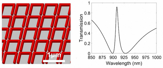
The geometry of the designed Si metamaterial structure deposited on a quartz substrate is illustrated in Figure 1a, which is arranged periodically in free space. Each unit cell depicted in Figure 1b comprises two vertical nanoscale bars and one horizontal nanoscale bar. The period of one unit structure is P = 615 nm in both x and y directions. The horizontal bar acts as a dipole antenna and can be excited supporting a bright mode resonance when coupling to the incident electromagnetic wave (Figure 1c). Two vertical bars serve as a quadrupolar antenna which cannot be directly excited by the external light and support a dark mode (Figure 1c). The dark mode resonator can only be excited by the near-field coupling with the bright mode resonator. When the plane wave is incident along the negative direction of the z axis with polarization along the x axis, the destructive interference between the bright mode and the dark mode leads to a narrow transmission window shown in Figure 1c, displaying a characteristic EIT-like behavior. The transmission peak is located at 908.5 nm with a high transmittance of 92%. The two transmission dips are located at 898.5 nm and 928 nm, respectively. The Q-factor can be calculated by the following formula:
where λ0 is the wavelength of transmission peak at the EIT-like window, and the FWHM is the full width at half maximum of transmission peak. The FWHM is 7 nm, and the calculated Q-factor is 130. It should be noted that when fixing the lengths and widths of the three nanoscale bars (see captions in Figure 1a) the thickness of the bars has an optimal value of 110 nm. When further reducing or increasing the thickness the FWHM of EIT transmission peak will become wider, and as a result the Q-factor will be reduced and the sensing performing of the Si metamaterial will be deteriorated.
To better understand the underlying physical mechanism of EIT-like effect in the proposed metamaterial structure, the field distribution maps in the x-y plane are plotted in Figure 2. The electric field distributions at transmission dips of 898.5 nm and 928 nm are shown in Figure 2a,b, respectively. It is seen that the horizontal nanoscale bar is mainly excited by the incident light. The emergence of the dipole mode with two nodes of electric fields at two tips of the bar and displacement currents along the horizontal nanoscale bar can hardly induce the resonance of two vertical nanoscale bars, leading to the transmission dips. Figure 2c shows the electric field distribution at transmission peak of 908.5 nm. The near-field resonant coupling between the two resonators causes the bright mode to couple energetically to the dark mode, which produces the destructive interference and achieve the EIT transmission peak, and suppresses the radiation of the dipole mode oscillation in the horizontal bar [32]. The quadrupole mode with three electric field nodes (two at the tips of the bars and one at the inner side of the bars) along the vertical Si bars is clearly observed. It is obvious that the induced surface field intensity at the peak is stronger than those at two dips. Furthermore, the high refractive index contrast between air and the all-dielectric metamaterial makes the local electric field on the edges of the structure stronger. All in all, the damping of radiation loss and high refractive index contrast are helpful for the metamaterials to achieve high transmission.
Next we investigated the effect of the period size of the unit structure on the EIT-like transmission window and Q-factor, the simulated transmission spectra with different period sizes are shown in Figure 3a. It is clear that although the transmittance does not change much, the resonance peak shifts towards the long wavelength and the FWHM of the EIT peak becomes wider as the period size increases, which indicates that the coupling coefficient decreases, resulting in a decrease in the Q-factor, as is shown in Figure 3b. The Si metamaterials with period of smaller than 615 nm were also checked. However, the near field interaction of nearby unit cells occurs due to the close distance between them when the period is smaller than 615 nm, which results in an off-resonance coupling between the dipole mode of the horizontal bar and the quadrupole mode of two vertical bars with an asymmetric shape of EIT transmission peak. Therefore, it can be found that the optimal period size is 615 nm.
The generation of EIT depends on the coherent interaction of the bright mode resonator and the dark mode resonator, and the incident polarization angle θ plays a key role in the effective excitation of the bright mode resonance [28]. In order to explore the effect of incident polarization angle on the EIT-like response of the dielectric metamaterial, the transmission spectra for the metamaterial with different incident polarization angles are demonstrated in Figure 4. The transmittance decreases as the angle θ changes from 0° to 90°, accompanied by a negligible shift of the transmission peak towards the short wavelength. When the angle increases to 90°, the transmission peak disappears completely, and only a transmission dip is observed. This is because when the incident electric field is parallel to the vertical bars, the bright mode dipole resonance of the horizontal bar cannot be excited while the dipole resonance of the dark mode resonator can be excited. However, the bright mode resonator cannot be excited by the dark mode dipole resonance, leading to the EIT peak vanishing [33].
The group velocity of light in a medium depends on the dispersion property of the medium which is the change of refractive index with the frequency of light. Due to the absorption and refraction properties of the medium are correlative, EIT must change the refractive index of the system when changing the absorption property [34]. The propagation velocity of wave decreases with the increase of group refractive index. A strong dispersion occurs due to the continuous steep change of phase in the transmission window, and this change reflects the speed of wave propagation. Therefore, the analogue of EIT is usually concomitant with slow-light effect [35,36]. The group delay is used to describe the slow-light effect and is defined as [37]:
where is the transmission phase shift. And the corresponding group index is defined as
where c is the velocity of light in free space, and are group velocity and delay time in the metamaterial respectively, and D is the thickness of the metamaterial. Figure 5a clearly shows that there are two frequency segments in the transmission phase spectrum, which are caused by anomalous phase dispersion and normal phase dispersion respectively [38]. The corresponding group index can reach 2035 due to strong dispersion of the transmission phase, which is shown in Figure 5b. The maximum optical delay indicated in Figure 5c is 0.75 ps in the transmission window. These values indicates that the proposed Si metamaterial can be used in efficient slow-light devices.
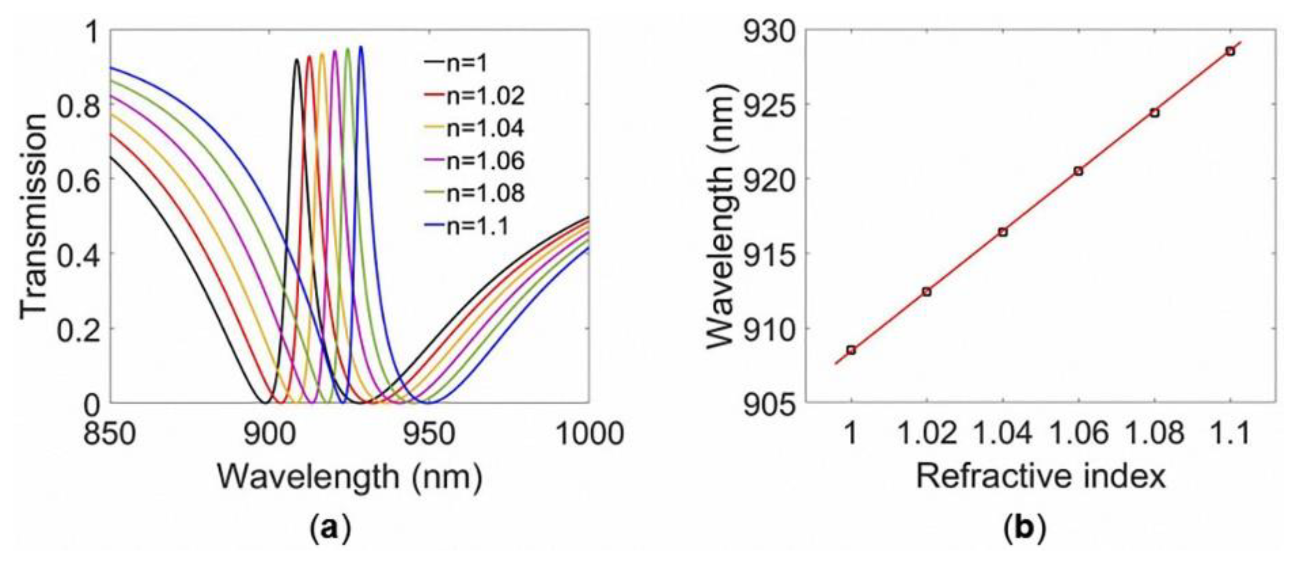
Optical sensing is also a potential application of the EIT metamaterial. When the refractive index of the surrounding medium changes (such as different liquids), the transmission peak tends to shift. Figure 6a shows the simulated transmission spectra of the designed dielectric metamaterial which immersed in different media with refractive index ranging from 1 to 1.1. It is clear that the peak position shifts towards the long wavelength despite the index changes very small. The figure-of-merit is an important parameter used to evaluate the sensing property and is determined as [39]
where is the sensitivity towards the environment refractive index, and is the resonance linewidth of the EIT-like transmission window. A linear fit between the wavelength shift of the transmission peak and the external refractive index is shown in Figure 6b, and the slope of the linear fit gives a sensitivity S of 203 nm/RIU. The corresponding FOM is 29 and is higher than Fano-resonant plasmonic sensors in the previous work [40,41,42].
4. Conclusions
We have numerically investigated the EIT-like phenomena in the proposed all-dielectric Si metamaterial. A characteristic EIT-like resonance peak with the high Q-factor and the high transmission is observed due to the coupling and interference between the bright mode supported by the horizontal nanoscale bar and the dark mode supported by the two vertical nanoscale bars. A nanoscale metamaterial refractive index sensor with high sensitivity and FOM has been achieved. The proposed Si metamaterials have a simple shape and can be easily fabricated by electron beam lithography [23,24,25,27]. The excellent optical performance enable the dielectric Si metamaterial with a wide range of potential applications including slow-light devices, sensing and storage of quantum information.
Author Contributions
B.W. and E.W. conceived and supervised all the simulation; M.Q. performed the simulation; M.Q., C.P. and Y.C. analyzed the data; Q.M. and S.L. contributed to the simulation software usage; M.Q. and B.W. wrote the manuscript; B.W. and E.W. revised the manuscript.
Funding
This research was funded by the National Nature Science Foundation of China (11674099, 61378033 and 11621404), Natural Science Foundation of Shanghai (16ZR1409400), Shuguang Program (15SG22), Shanghai International Cooperation Project (16520710600), and the 111 Project (B12024).
Conflicts of Interest
The authors declare no conflict of interest.
References
- Fleischhauer, M.; Imamoglu, A.; Marangos, J.P. Electromagnetically induced transparency: Optics in coherent media. Rev. Mod. Phys. 2005, 77, 633–673. [Google Scholar] [CrossRef] [Green Version]
- Harris, S.E. Electromagnetically induced transparency. Phys. Today 1997, 50, 36–42. [Google Scholar] [CrossRef]
- Boller, K.J.; Imamoğlu, A.; Harris, S.E. Observation of electromagnetically induced transparency. Phys. Rev. Lett. 1991, 66, 2593–2596. [Google Scholar] [CrossRef] [PubMed]
- Dong, Z.G.; Liu, H.; Cao, J.X.; Li, T.; Wang, S.M.; Zhu, S.N.; Zhang, X. Enhanced sensing performance by the plasmonic analog of electromagnetically induced transparency in active metamaterials. Appl. Phys. Lett. 2010, 97, 114101. [Google Scholar] [CrossRef] [Green Version]
- Liu, N.; Weiss, T.; Mesch, M.; Langguth, L.; Eigenthaler, U.; Hirscher, M.; Sönnichsen, C.; Giessen, H. Planar metamaterial analogue of electromagnetically induced transparency for plasmonic sensing. Nano Lett. 2009, 10, 1103–1107. [Google Scholar] [CrossRef] [PubMed]
- Khurgin, J.B. Optical buffers based on slow light in electromagnetically induced transparent media and coupled resonator structures: Comparative analysis. J. Opt. Soc. Am. B 2005, 22, 1062–1074. [Google Scholar] [CrossRef]
- Hau, L.V.; Harris, S.E.; Dutton, Z.; Behroozi, C.H. Light speed reduction to 17 metres per second in an ultracold atomic gas. Nature 1999, 397, 594–598. [Google Scholar] [CrossRef]
- Cong, J.W.; Zheng, G.G.; Yun, B.F.; Zhou, Z.Q. Simultaneous enhancement of bandwidth and group index of slow light via metamaterial induced transparency with double bright resonators. IEEE J. Sel. Top. Quantum Electron. 2015, 21, 295–300. [Google Scholar] [CrossRef]
- Papasimakis, N.; Fedotov, V.A.; Zheludev, N.I.; Prosvirnin, S.L. Metamaterial analog of electromagnetically induced transparency. Phys. Rev. Lett. 2008, 101, 253903. [Google Scholar] [CrossRef] [PubMed]
- Zhu, L.; Meng, F.Y.; Fu, J.H.; Wu, Q.; Hua, J. Multi-band slow light metamaterial. Opt. Express 2012, 20, 4494–4502. [Google Scholar] [CrossRef] [PubMed]
- Liu, C.; Dutton, Z.; Behroozi, C.H.; Hau, L.V. Observation of coherent optical information storage in an atomic medium using halted light pulses. Nature 2001, 409, 490–493. [Google Scholar] [CrossRef] [PubMed]
- Fleischhauer, M.; Lukin, M.D. Dark-state polaritons in electromagnetically induced transparency. Phys. Rev. Lett. 2000, 84, 5094–5097. [Google Scholar] [CrossRef] [PubMed]
- Zhu, Z.H.; Yang, X.; Gu, J.Q.; Jiang, J.; Yue, W.S.; Tian, Z.; Tonouchi, M.; Han, J.G.; Zhang, W.L. Broadband plasmon induced transparency in terahertz metamaterials. Nanotechnology 2013, 24, 214003. [Google Scholar] [CrossRef] [PubMed]
- Shalaev, V.M. Optical negative-index metamaterials. Nat. Photonic 2007, 1, 41–48. [Google Scholar] [CrossRef]
- Soukoulis, C.M.; Linden, S.; Wegener, M. Negative refractive index at optical wavelengths. Science 2007, 315, 47–49. [Google Scholar] [CrossRef] [PubMed]
- Luk’yanchuk, B.; Zheludev, N.I.; Maier, S.A.; Halas, N.J.; Nordlander, P.; Giessen, H.; Chong, C.T. The Fano resonance in plasmonic nanostructures and metamaterials. Nat. Mater. 2010, 9, 707–715. [Google Scholar] [CrossRef] [PubMed]
- Zhang, S.; Genov, D.A.; Wang, Y.; Liu, M.; Zhang, X. Plasmon-induced transparency in metamaterials. Phys. Rev. Lett. 2008, 101, 047401. [Google Scholar] [CrossRef] [PubMed]
- Zhang, J.J.; Xiao, S.S.; Jeppesen, C.; Kristensen, A.; Mortensen, N.A. Electromagnetically induced transparency in metamaterials at near-infrared frequency. Opt. Express 2010, 18, 17187–17192. [Google Scholar] [CrossRef] [PubMed]
- Muhammad, N.; Khan, A.D. Electromagnetically Induced Transparency and Sharp Asymmetric Fano Line Shapes in All-Dielectric Nanodimer. Plasmonics 2017, 12, 1399–1407. [Google Scholar] [CrossRef]
- Sun, B.; Zhao, L.X.; Wang, C.; Yi, X.Y.; Liu, Z.Q.; Wang, G.H.; Li, J.M. Tunable Fano resonance in E-shape plasmonic nanocavities. J. Phys. Chem. C 2014, 118, 25124–25131. [Google Scholar] [CrossRef]
- Yang, Y.M.; Wang, W.Y.; Moitra, P.; Kravchenko, I.I.; Briggs, D.P.; Valentine, J. Dielectric meta-reflectarray for broadband linear polarization conversion and optical vortex generation. Nano Lett. 2014, 14, 1394–1399. [Google Scholar] [CrossRef] [PubMed]
- O’Brien, S.; Pendry, J.B. Photonic band-gap effects and magnetic activity in dielectric composites. J. Phys. Condens. Matter 2002, 14, 4035–4044. [Google Scholar] [CrossRef] [Green Version]
- Yang, Y.M.; Kravchenko, I.I.; Briggs, D.P.; Valentine, J. All-dielectric metasurface analogue of electromagnetically induced transparency. Nat. Commun. 2014, 5, 5753. [Google Scholar] [CrossRef] [PubMed] [Green Version]
- Yang, Y.M.; Wang, W.Y.; Boulesbaa, A.; Kravchenko, I.I.; Briggs, D.P.; Puretzky, A.; Geohegan, D.; Valentine, J. Nonlinear Fano-resonant dielectric metasurfaces. Nano Lett. 2015, 15, 7388–7393. [Google Scholar] [CrossRef] [PubMed]
- Liu, H.Z.; Guo, C.; Vampa, G.; Zhang, J.L.; Sarmiento, T.; Xiao, M.; Bucksbaum, P.H.; Vučković, J.; Fan, S.H.; Reis, D.A. Enhanced high-harmonic generation from an all-dielectric metasurface. Nat. Phys. 2018, 1. [Google Scholar] [CrossRef]
- Zhang, Y.B.; Liu, W.W.; Li, Z.C.; Li, Z.; Cheng, H.; Chen, S.Q.; Tian, J.G. High-quality-factor multiple Fano resonances for refractive index sensing. Opt. Express 2018, 43, 1842–1845. [Google Scholar] [CrossRef] [PubMed]
- Wu, C.; Arju, N.; Kelp, G.; Fan, J.A.; Dominguez, J.; Gonzales, E.; Tutuc, E.; Brener, I.; Shvets, G. Spectrally selective chiral silicon metasurfaces based on infrared Fano resonances. Nat. Commun. 2014, 5, 3892. [Google Scholar] [CrossRef] [PubMed] [Green Version]
- Wei, Z.C.; Li, X.P.; Zhong, N.F.; Tan, X.P.; Zhang, X.M.; Liu, H.Z.; Meng, H.Y.; Liang, R.S. Analogue electromagnetically induced transparency based on low-loss metamaterial and its application in nanosensor and slow-light device. Plasmonics 2017, 12, 641–647. [Google Scholar] [CrossRef]
- Han, B.; Li, X.; Sui, C.; Diao, J.; Jing, X.; Hong, Z. Analog of electromagnetically induced transparency in an E-shaped all-dielectric metasurface based on toroidal dipolar response. Opt. Mater. Express 2018, 8, 2197–2207. [Google Scholar] [CrossRef]
- Taflove, A.; Hagness, S.C. Computational Electrodynamics: The Finite-Difference Time-Domain Method, 3rd ed.; Artech House: Boston, MA, USA, 2005; pp. 1–30. ISBN 978-1-58053-832-9. [Google Scholar]
- Palik, E.D. Handbook of Optical Constants of Solids, 1st ed.; Academic Press: New York, NY, USA, 1985; pp. 547–569. ISBN 978-0-08-054721-3. [Google Scholar]
- Jenkins, S.D.; Ruostekoski, J. Metamaterial transparency induced by cooperative electromagnetic interactions. Phys. Rev. Lett. 2013, 111, 147401. [Google Scholar] [CrossRef] [PubMed]
- He, J.N.; Wang, J.Q.; Ding, P.; Fan, C.Z.; Arnaut, L.R.; Liang, E.J. Optical switching based on polarization tunable plasmon-induced transparency in disk/rod hybrid metasurfaces. Plasmonics 2015, 10, 1115–1121. [Google Scholar] [CrossRef]
- Pitchappa, P.; Manjappa, M.; Ho, C.P.; Singh, R.; Singh, N.; Lee, C. Active control of electromagnetically induced transparency analog in terahertz MEMS metamaterial. Opt. Mater. 2016, 4, 541–547. [Google Scholar] [CrossRef]
- Zhang, F.L.; Huang, X.C.; Zhao, Q.; Chen, L.; Wang, Y.; Li, Q.; He, X.; Li, C.; Chen, K. Fano resonance of an asymmetric dielectric wire pair. Appl. Phys. Lett. 2014, 105, 172901. [Google Scholar] [CrossRef]
- Gu, J.Q.; Singh, R.; Liu, X.J.; Zhang, X.Q.; Ma, Y.F.; Zhang, S.; Maier, S.A.; Tian, Z.; Azad, A.K.; Chen, H.T.; et al. Active control of electromagnetically induced transparency analogue in terahertz metamaterials. Nat. Commun. 2012, 3, 1151. [Google Scholar] [CrossRef] [PubMed]
- Lu, H.; Liu, X.M.; Mao, D. Plasmonic analog of electromagnetically induced transparency in multi-nanoresonator-coupled waveguide systems. Phys. Rev. A 2012, 85, 053803. [Google Scholar] [CrossRef]
- Wang, J.Q.; Yuan, B.H.; Fan, C.Z.; He, J.N.; Ding, P.; Xue, Q.Z.; Liang, E.J. A novel planar metamaterial design for electromagnetically induced transparency and slow light. Opt. Express 2013, 21, 25159–25166. [Google Scholar] [CrossRef] [PubMed]
- Anker, J.N.; Hall, W.P.; Lyandres, O.; Shah, N.C.; Zhao, J.; Van Duyne, R.P. Biosensing with plasmonic nanosensors. Nat. Mater. 2008, 7, 442–453. [Google Scholar] [CrossRef] [PubMed]
- Hu, J.; Lang, T.T.; Hong, Z.; Shen, C.Y.; Shi, G.H. Comparison of Electromagnetically Induced Transparency Performance in Metallic and All-Dielectric Metamaterials. J. Lightw. Technol. 2018, 36, 2083–2093. [Google Scholar] [CrossRef]
- Zhang, S.P.; Bao, K.; Halas, N.J.; Xu, H.X.; Nordlander, P. Substrate-induced Fano resonances of a plasmonic nanocube: A route to increased-sensitivity localized surface plasmon resonance sensors revealed. Nano Lett. 2011, 11, 1657–1663. [Google Scholar] [CrossRef] [PubMed]
- Lassiter, J.B.; Sobhani, H.; Fan, J.A.; Kundu, J.; Capasso, F.; Nordlander, P.; Halas, N.J. Fano resonances in plasmonic nanoclusters: Geometrical and chemical tunability. Nano Lett. 2010, 10, 3184–3189. [Google Scholar] [CrossRef] [PubMed]
Figure 1.
(a) Schematic of the dielectric metamaterial structure deposited on a quartz substrate. (b) Schematic of a metamaterial unit cell with the period size P of 615 nm comprising two vertical silicon nanoscale bars and one horizontal silicon nanoscale bar. The geometrical parameters are: a = 580 nm, b = 590 nm, c = 510 nm, d = 80 nm, e = 80 nm, h1 = 110 nm, h2 = 100 nm. (c) Simulated transmission spectra of the metamaterial structure as well as the bright and dark modes supported by the horizontal and vertical bars respectively.
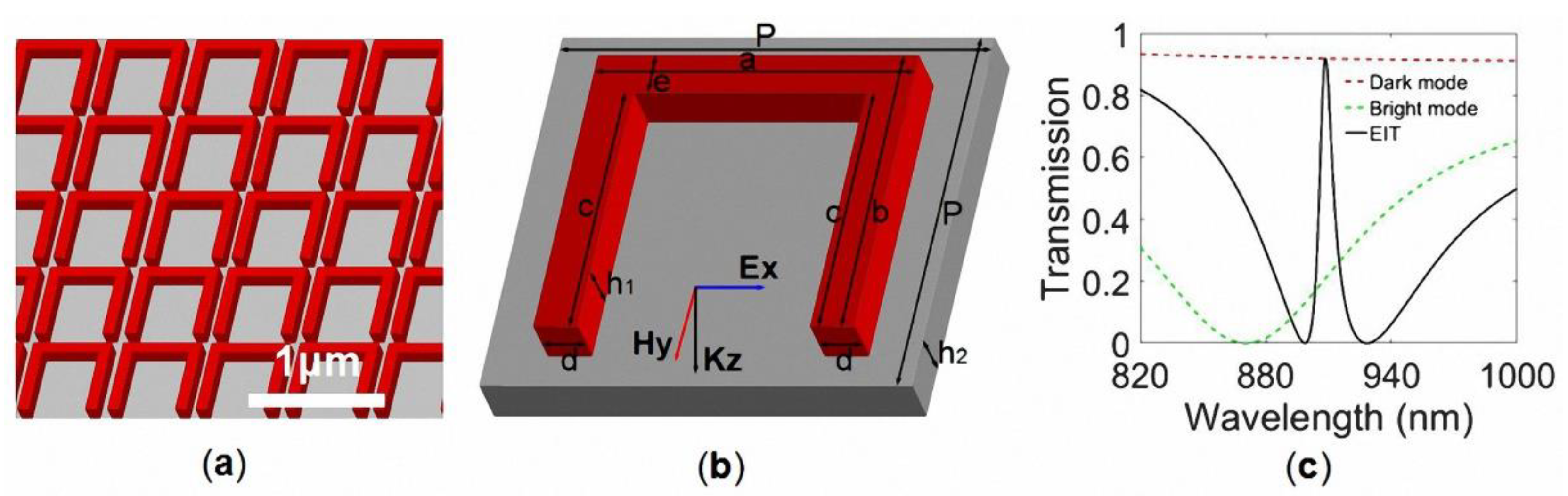
Figure 2.
Electric field distributions of the dielectric metamaterial at different wavelengths. (a), (b) and (c) correspond to the wavelengths of 898.5 nm, 928 nm and 908.5 nm, respectively. The other geometrical parameters are the same as in Figure 1b.
Figure 2.
Electric field distributions of the dielectric metamaterial at different wavelengths. (a), (b) and (c) correspond to the wavelengths of 898.5 nm, 928 nm and 908.5 nm, respectively. The other geometrical parameters are the same as in Figure 1b.
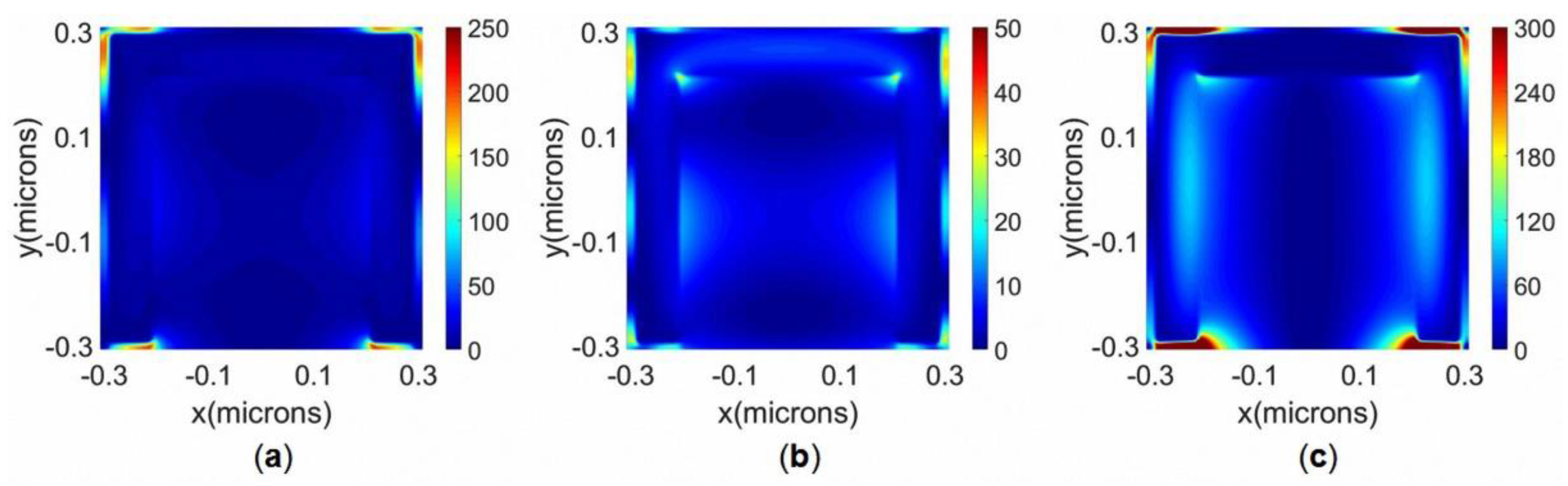
Figure 3.
(a) Simulated transmission spectra with different period sizes. (b) The Q-factors of the EIT-like resonance with different period sizes.
Figure 3.
(a) Simulated transmission spectra with different period sizes. (b) The Q-factors of the EIT-like resonance with different period sizes.

Figure 4.
Simulated transmission spectra with different incident polarization angles.
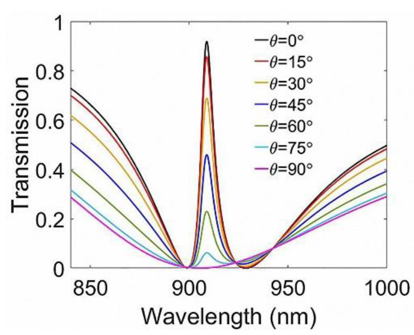
Figure 5.
Simulated transmission phase shift (a), group index (b), and group delay (c) of the dielectric metamaterial with geometrical parameters are the same as shown in Figure 1b.
Figure 5.
Simulated transmission phase shift (a), group index (b), and group delay (c) of the dielectric metamaterial with geometrical parameters are the same as shown in Figure 1b.

Figure 6.
(a) Simulated transmission spectra of the metamaterial structure with refractive index ranging from 1 to 1.1. (b) The EIT-like peak wavelength of the metamaterial structure as a function of refractive index. The squares are the measured data, and the red line is the linear fit.
Figure 6.
(a) Simulated transmission spectra of the metamaterial structure with refractive index ranging from 1 to 1.1. (b) The EIT-like peak wavelength of the metamaterial structure as a function of refractive index. The squares are the measured data, and the red line is the linear fit.

© 2018 by the authors. Licensee MDPI, Basel, Switzerland. This article is an open access article distributed under the terms and conditions of the Creative Commons Attribution (CC BY) license (http://creativecommons.org/licenses/by/4.0/).
Share and Cite
MDPI and ACS Style
Qin, M.; Pan, C.; Chen, Y.; Ma, Q.; Liu, S.; Wu, E.; Wu, B. Electromagnetically Induced Transparency in All-Dielectric U-Shaped Silicon Metamaterials. Appl. Sci. 2018, 8, 1799. https://doi.org/10.3390/app8101799
AMA Style
Qin M, Pan C, Chen Y, Ma Q, Liu S, Wu E, Wu B. Electromagnetically Induced Transparency in All-Dielectric U-Shaped Silicon Metamaterials. Applied Sciences. 2018; 8(10):1799. https://doi.org/10.3390/app8101799
Chicago/Turabian StyleQin, Mengyao, Chengda Pan, Yu Chen, Qiang Ma, Shikang Liu, E Wu, and Botao Wu. 2018. "Electromagnetically Induced Transparency in All-Dielectric U-Shaped Silicon Metamaterials" Applied Sciences 8, no. 10: 1799. https://doi.org/10.3390/app8101799
Note that from the first issue of 2016, this journal uses article numbers instead of page numbers. See further details here.