Quality-Improved GaN Epitaxial Layers Grown on Striped Patterned Sapphire Substrates Ablated by Femtosecond Laser
by
Yichao Xu
1, 
Jun Zou
2,*,
Xiaoyan Lin
2,*,
Wenjuan Wu
2,
Wenbo Li
3,
Bobo Yang
2 and
Mingming Shi
2 1
School of Materials Science and Engineering, Shanghai Institute of Technology, Shanghai 201418, China
2
School of Sciences, Shanghai Institute of Technology, Shanghai 201418, China
3
Zhejiang Emitting Optoelectronic Technology Co., Ltd., Jiaxing 314100, China
*
Authors to whom correspondence should be addressed.
Appl. Sci. 2018, 8(10), 1842; https://doi.org/10.3390/app8101842
Submission received: 29 August 2018
/
Revised: 26 September 2018
/
Accepted: 28 September 2018
/
Published: 8 October 2018
(This article belongs to the Special Issue Ultrafast Laser Pulses)
Abstract
:In this work, we propose a new approach to create striped patterned sapphire substrate (PSS) under the circumstance that grooved patterned sapphire substrate technology exhibits more potential to reduce dislocation density in GaN (gallium nitride) epilayers. The striped grooves of patterned sapphire substrate are ablated by femtosecond laser. After the process of metal-organic chemical vapor deposition (MOCVD) method, the c-plane GaN epitaxial layers grown on striped PSS have larger crystallite size, which brings much less crystal boundary. There is much less compressive stress between the GaN crystals which improves the smoothness and compactness of GaN epilayers. This result demonstrates a significant improvement in the crystallinity of the c-plane GaN epitaxial layers grown on striped PSS.
1. Introduction
Recently, the application of sapphire in manufacturing light emitting diodes (LEDs) has become increasingly popular in the LEDs market ascribe to the low fabrication cost. Nonetheless, large lattice mismatch (15%) and thermal expansion coefficient mismatch (25%) between GaN (gallium nitride) films and sapphire substrates result in high dislocation densities and residual stress, which seriously decrease the internal quantum efficiency and affect the optical and electrical performance of the GaN-based LED [1,2]. To improve the performance of the films grown on sapphire substrate, a lot of methods have been put forward, such as the use of buffer layers [3], epitaxial lateral over-growth (ELOG) technology [4], Bragg reflecting layers [5], photonic crystals [6,7], surface coarsening [8,9], and flip-chip technique [10], a more efficient solution provided by some researchers is using patterned sapphire substrate (PSS) [11,12]. For instance, it includes grooved type [13], hemispherical type [14], conic type [15] and hexagonal type [16] PSS (patterned sapphire substrate). Among these patterns, grooved PSS, which is widely applied to PSS applications, exhibits more potential to improve LED efficacy along with its effectiveness to reduce dislocation density [17]. Meanwhile, there has been little study about the PSS created by femtosecond laser. Under this circumstance, we proposed a new approach to create striped grooved PSS by laser ablation. In this study, we describe the fabrication and characteristics of the c-plane GaN epitaxial layers grown on striped PSS and demonstrate the improvement in the crystallinity of striped PSS sample, compared with the traditional planar sample.
2. Materials and Methods
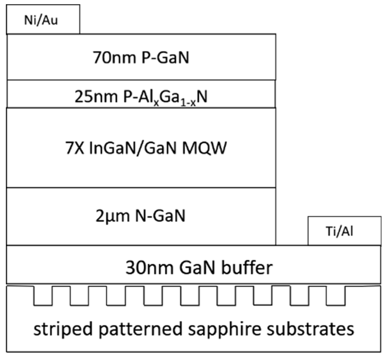
The striped PSS was fabricated by femtosecond laser ablation with a peak wavelength of 780 nm, a repetition rate of 1000 Hz, a pulse duration of 150 fs and a pulse energy of 2 mJ. The femtosecond laser beam was focused on the sapphire substrate by a 75 mm spherical lens, with a spot size of 40 µm [18]. The Figure 1 illustrates the InxGa1−xN/GaN LED structures grown on striped PSS. The InxGa1−xN/GaN LED was fabricated by the low-pressure vertical MOCVD (metal-organic chemical vapor deposition) method. In the process of MOCVD, we used trimethylindium (TMIn), trimethylgallium (TMGa) and ammonia (NH3) as the source materials of In, Ga and N. Bicyclopentadienyl magnesium (Cp2Mg) and silane (SiH4) were chosen as the p-type and n-type doping sources. High-purity N2 is employed as the carrier gas. The substrates are firstly heated to 1050 °C within the ambient H2, followed by the 6-min baking process to purge away oxides from substrates. Nitrogen-treatment is then carried out within NH3 at 530 °C followed by the 4-min growth of GaN buffer layers. Afterwards, the chamber temperature is raised to 1020 °C for the recrystallization of GaN buffer layers. The GaN 3D islands nucleation lasts for 55 min at 1020 °C subsequently. Finally, the 28-min GaN recovery layers are grown at 1105 °C, respectively. The LED structure was made up with 70 nm Mg-doped p-type GaN, 25 nm p-type AlGaN (aluminum gallium nitride), seven period multi quantum wells (MQWs), 2 µm Si-doped n-type layer, 30 nm buffer layer of GaN, striped PSS and two electrodes from top to bottom. To be specific, the p- and n-electrodes are made by Ni/Au and Ti/Al, respectively.
Scanning electron microscopy (SEM) images were taken on a Hitachi S-3400N field emission scanning electron microscope (Hitachi, Tokyo, Japan). The crystal structures of GaN epitaxial layers were confirmed by X-ray diffraction (XRD) method (Rigaku, Ultima IV, Japan) with Cu Kα radiation (k = 0.154178 nm) over a 2θ range from 20° to 80° at a scanning rate of 0.02°/step and 4°/min. To investigate the stress in GaN epitaxial layers grown on both planar substrate and striped PSS, micro-Raman scatting experiments, performed with multichannel modular triple Raman systems (Horiba Jobin-Yvon LabRAM Aramis, Paris, France), are carried out in backscatting geometry at room temperature. The Raman spectra was measured by focusing the 514.5 nm excitation line of Ar+ laser on the sample and detected the backscattered light. The optical absorption spectrum was examined with an Agilent Cary 5000 UV/VIS/NIR spectrophotometer (Agilent Technologies, Santa Clara, CA 95051, United States).
3. Results and Discussion
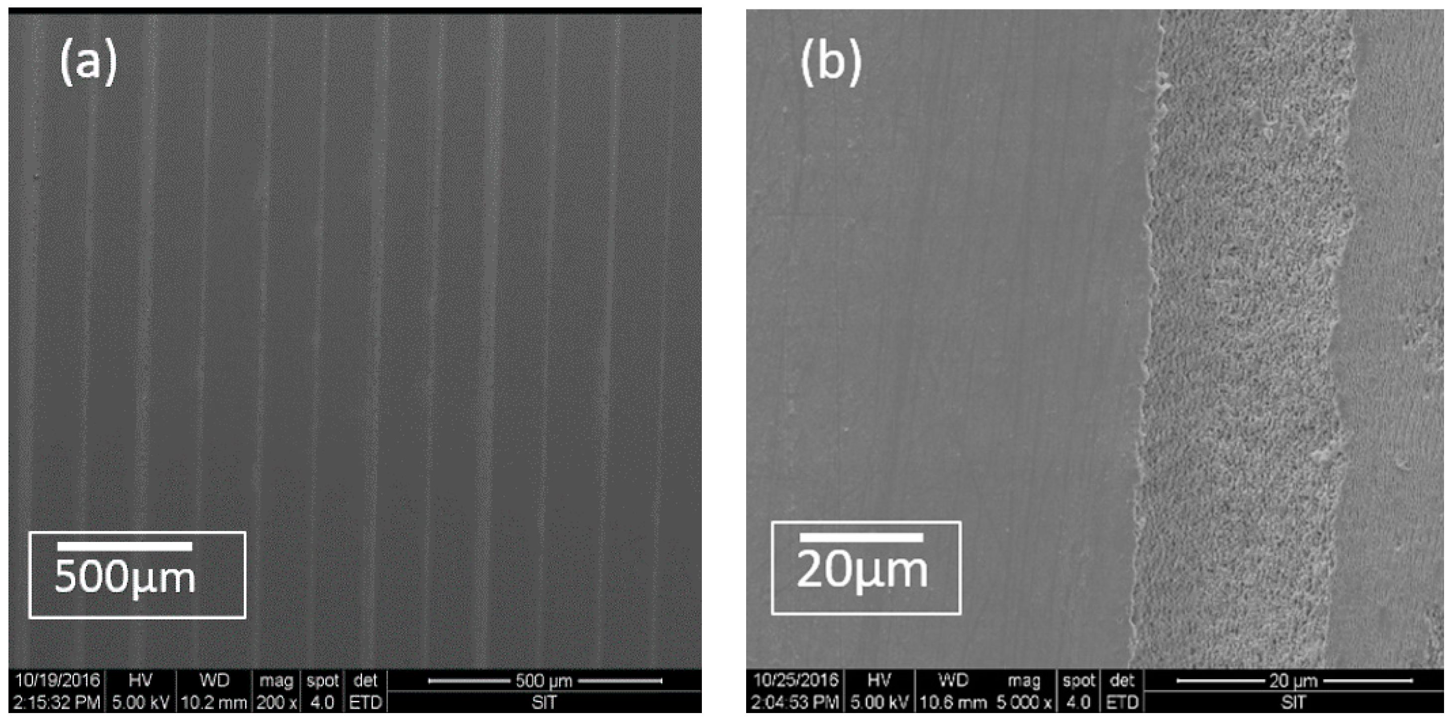
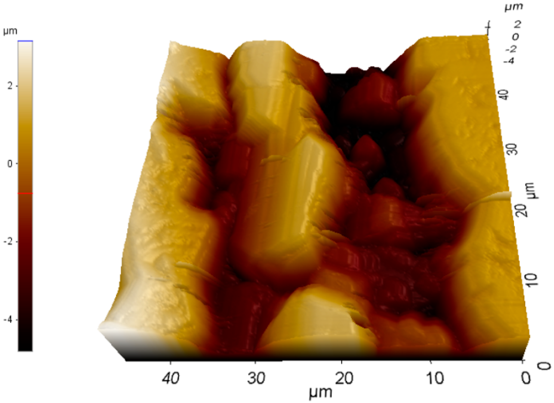
The striped grooves can be seen luminously in Figure 2 by scanning electron microscopy (SEM) measurement. Figure 3 shows the AFM (atomic force microscope) images of surface three-dimensional topography of the striped grooves. There are many rugged bumps at the bottom of the groove. The average depth and width of the grooves are approximately 6 µm and 10 µm.
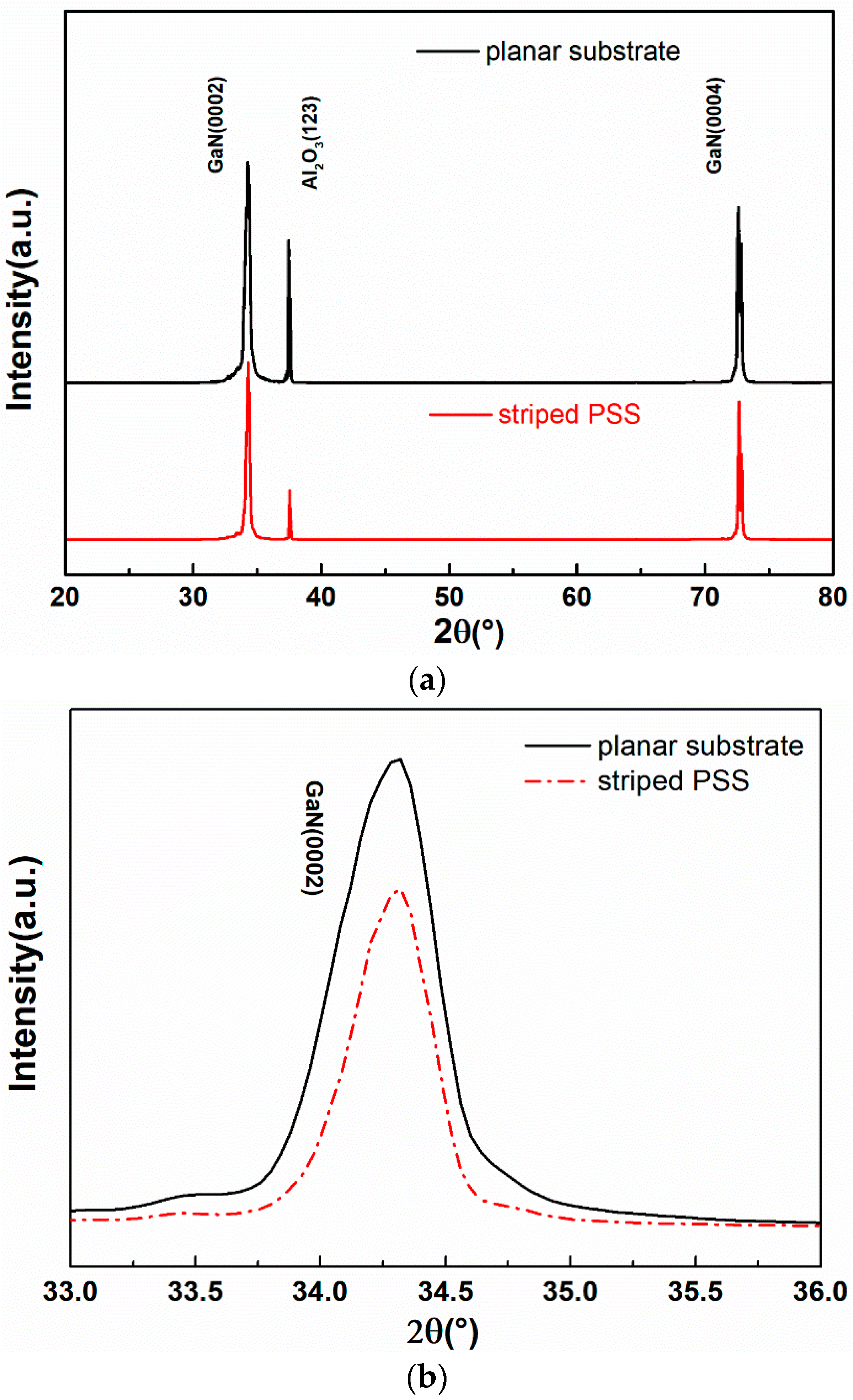
Figure 4a illustrates the XRD pattern of c-plane GaN films grown on striped PSS, compared with those grown on planar substrate. From Figure 4a, red line represents the XRD pattern on striped PSS while black line corresponds to that on planar substrate and their peaks locate at the same position. The sharp peaks emerging at 34.28° and 72.63° have been attached to the GaN (0002) plane and GaN (0004) plane, respectively, which illustrates that the GaN grown on sapphire substrates is predominately c-plane orientation [19]. The peak located at 37.50° is corresponded to Al2O3 (123) substrate. No other phases have been observed in this pattern, so it illustrates the GaN epilayers grown on both substrates have a relatively high purity. Crystalline quality of the GaN (0002) can be accessed by the full width at half maximum (FWHM) values and crystal size. From Figure 4b rocking curves, the FWHM values of the two samples can be calculated to be 0.302° and 0.370°, corresponding to the striped sample and planar sample symmetrically. And the average crystallite size of the GaN can be deployed to calculated by Scherrer equation [20]:
where D is the crystallite size relative to the peak width in radians, K is a constant, λ represents the X-ray wavelength, β corresponds to the FWHM value of the diffraction peak while θ is relative to the Bragg diffraction angle of c-plane GaN. By calculation, the crystallite size of GaN films grown on striped sample and planar substrate are 31.3 and 25.6 nm, respectively. Thus, the crystallite size of striped sample is much larger than that of planar sample. Additionally, in the nucleation process of GaN, as the crystal size increases, the crystal boundaries decrease, and there are more opportunities to generate binary and ternary phases within the crystal boundaries. Thus, compared with the planar sample, the GaN epilayers grown on striped PSS have less crystal boundary, which results in that smoothness and compactness of the c-plane GaN epilayers will be moderately improved. Therefore, crystalline quality of c-plane GaN epilayers have been improved by patterning striped sapphire substrate.
Moreover, XRD rocking curves are employed to calculate the threading dislocation density by the following equation [21]:
where ρ represents the threading dislocation density, β is the FWHM of the GaN (0002) XRD rocking curve, and b is the value of the Burgers vector. From Figure 4, the FWHM of planar sample is much larger than that of the striped PSS which gives a result that striped PSS will have less threading dislocation density according to equation above. Less threading dislocation density of striped PSS can also indicate the higher crystalline quality of c-plane GaN epilayers grown on striped PSS.
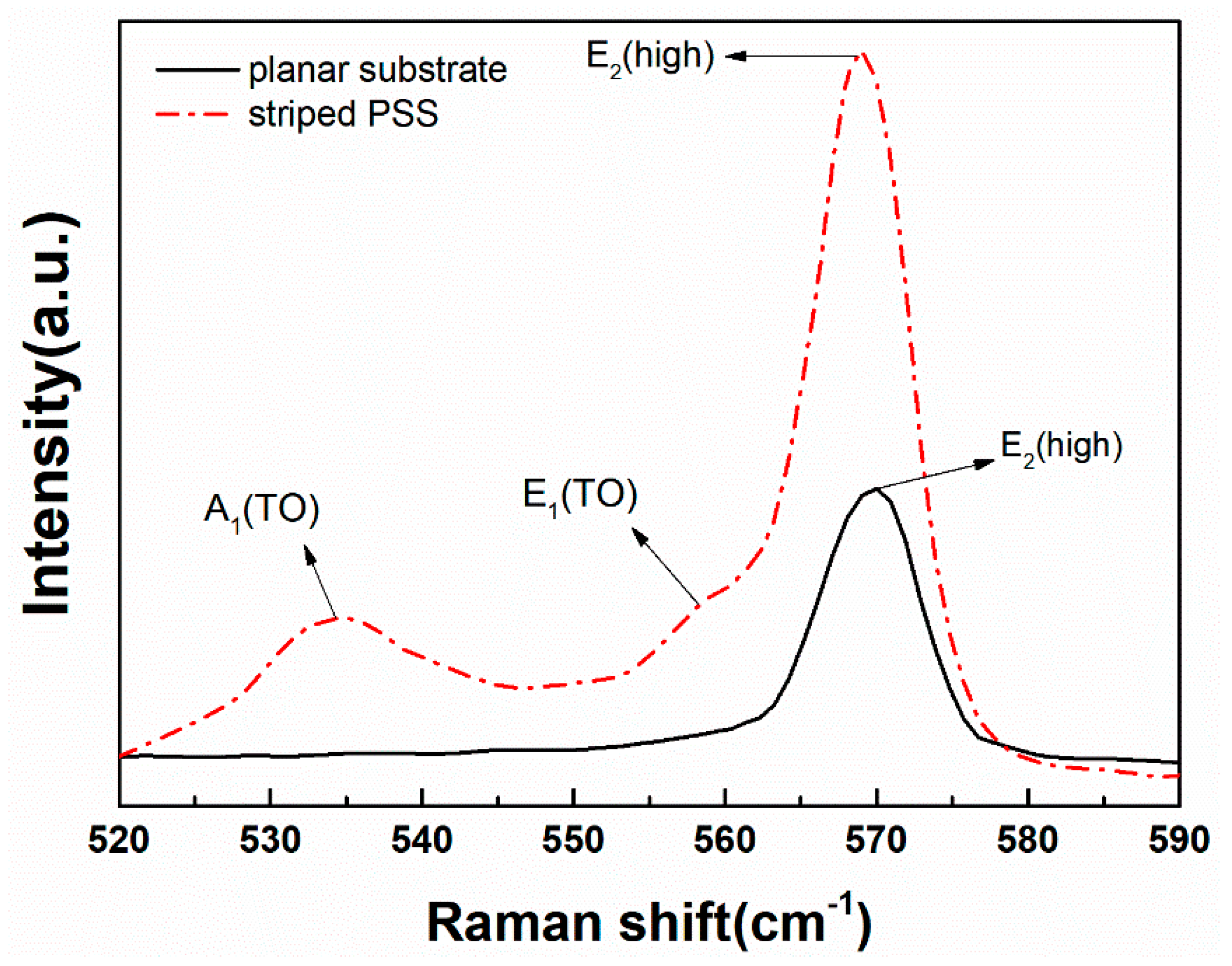
The Raman spectroscopy is also used to demonstrate the residual stress in GaN epitaxial layers [21]. Figure 5 illustrates the Raman spectra of different samples grown on planar substrate and striped PSS. The spectra consisted of a strong E2 (high) peak and A1 (LO) phonon peak, respectively, near 568 and 734 cm−1, which coincides well with the Raman selection rule for wurtzite GaN. Compared with the Raman spectrum of the sample plane, PSS sample striped clearly observed significantly enhanced scattering efficiency. Due to the introduction of surface disturbance surface of the microstructure, more efficient coupling of light scattering and multiple scattered radiation, the sample can be observed from the striped PSS significant increase in the Raman intensity. E2 (high) for monitoring the line width of phonons in crystal quality, and its frequency may be used to monitor the stress of the film [21]. From Table 1, the E2 (high) phonon peaks of the films grown on different substrates are observed at 568.8 and 569.9 cm−1, corresponding to the striped PSS and the planar substrate. The shift of E2 (high) phonon peak is the main indicator for the residual stress in wafers. Additionally, unstained GaN is characterized by standard E2 frequency of 568 cm−1 [22]. It appears compressive stress when E2 frequency is larger than the standard value. As we all know, the amount of stress relaxation can be calculated by the following equation [23,24]:
where σ represents the residual stress and ∆ω is the E2 (high) phonon peak shift. It can be seen from Table 1 that the E2 (high) phonon frequency of striped sample is shifted to 568.8 cm−1, while that of planar sample is shifted to 569.9 cm−1. Obviously, the two samples show a slight red shift by about 0.82 and 1.90 cm−1 corresponds to the compressive stress by an amount 0.19 Gpa and 0.45 Gpa, respectively for striped sample and planar sample. So, the compressive stress of striped sample is much smaller than that of planar sample. The value of striped sample demonstrates that the epilayers grown on striped PSS are almost fully relaxed. In contrast to those on planar substrate, as-grown epilayers on striped PSS have less lattice mismatch which can reduce dislocation in GaN films [25]. As we all know, high dislocations reduce the carrier mobility, reducing the minority carrier lifetime and depress the thermal conductivity [26]. Therefore, the result of FWHM also matches with the result of XRD which appears that the quality of GaN epitaxial layers grown on striped PSS has been improved.
The amount of stress estimated from the E2 (high) phonon peak shift relative to a 400 μm thick independent GaN without strain is displayed in Table 1.
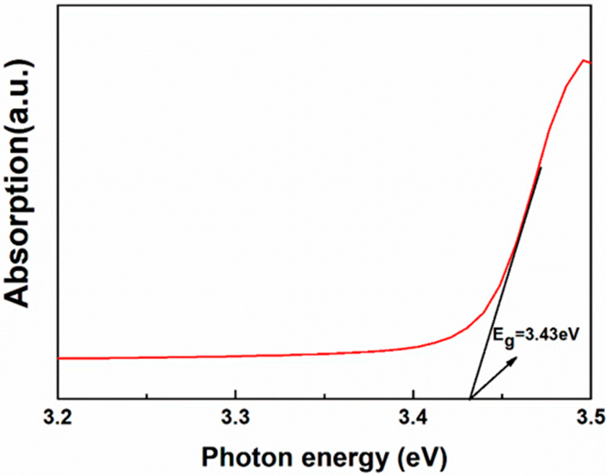
The crystallinity of the GaN films grown on striped PSS can also be researched by the absorption spectra. The transmittance of GaN films is about 80% in the wavelength range of 400–800 nm. From Figure 6, there is a sharp drop of the transmittance, which indicates the high crystallinity of the GaN epilayers. When GaN absorbs the light, the electrons in GaN can be activated and move from the valence band to the conduction band [27]. The amount of photon energy absorbed by GaN can be calculated by the following equation [28]:
where is a constant, represents the photon energy, stands for the optical band gap of thin wafer, and the index n relies on the type of transition. For GaN, the n used to be ½ [29]. can be deployed to calculate by the following equation:
In the equation, represents the transmittance and stands for film thickness. The optical band gap of GaN can be obtained from the plot in Figure 6. Prolong the tangent line to energy axis and the value of the intersection exactly becomes the band gap . From Figure 6, the band gap of the GaN on striped PSS is estimated to be 3.43 eV. For stoichiometric GaN films, the optical band gap used to be about 3.4 eV. Hence, the result is consistent with the result of Raman measurements and it also appears a red shift which gives evidence for the GaN films grown on striped PSS having higher crystallinity.
4. Conclusions
In this paper, we focus on the crystallinity of the c-plane GaN epitaxial layers grown on striped patterned sapphire substrates ablated by femtosecond laser. The surface morphology observed by SEM reveals the striped grooves in details which is the major factor to improve the crystallinity. By measuring the XRD, we obtained that the FWHM of striped sample is 0.302° which is much smaller than that of planar sample, while the crystallite size is 31.3 nm which is larger than that of the planar sample. Moreover, the little compressive stress is also found in GaN epitaxial layers by the measurement of Raman spectra. Compared with the planar substrate, the striped grooves help release the compressive stress and improve the crystallinity. The same result is also proved by the absorption spectra. The band gap of the striped PSS is estimated to be 3.43 eV. In conclusion, the PSS with striped grooves created by femtosecond laser ablation can improve the crystallinity of the c-plane GaN epitaxial layers.
Author Contributions
Conceptualization, X.L.; Methodology, J.Z.; Software, Y.X.; Validation, Y.X., W.L. and B.Y.; Formal Analysis, Y.X.; Investigation, Y.X.; Resources, J.Z.; Data Curation, Y.X.; Writing-Original Draft Preparation, Y.X.; Writing-Review & Editing, Y.X.; Visualization, M.S.; Supervision, W.W.; Project Administration, B.Y.; Funding Acquisition, J.Z.
Funding
This research was funded by (Enterprise-funded Latitudinal Research Projects) grant number (J2016-141, J2017-171, J2017-293, J2017-243) and (Science and Technology Planning Project of Zhejiang Province, China) grant number (2018C01046).
Conflicts of Interest
The authors declare no conflict of interest.
References
- Reed, M.D.; Kryliouk, O.M.; Mastro, M.A.; Anderson, T.J. Growth and characterization of single-crystalline gallium nitride using (100) LiAlO2 substrates. J. Cryst. Growth 2005, 274, 14–20. [Google Scholar] [CrossRef]
- Wang, W.; Yang, W. Epitaxial growth of GaN films on unconventional oxide substrates. J. Mater. Chem. 2014, 2, 9342–9358. [Google Scholar] [CrossRef]
- Le Vaillant, Y.M.; Bisaro, R. Caracterization of AIN buffer layers on (0001)-sapphire substrates. Mater. Sci. Eng. B 1997, 50, 32–37. [Google Scholar] [CrossRef]
- Sakai, A.; Sunakawa, H. Defect structure in selectively grown GaN films with low threading dislocation density. Appl. Phys. Lett. 1997, 71, 2259–2261. [Google Scholar] [CrossRef]
- Nakada, N.; Nakaji, M. Improved characteristics of InGaN multiple-quantum-well light-emitting diode by GaN/AlGaN distributed Bragg reflector grown on sapphire. Appl. Phys. Lett. 2000, 76, 1804–1806. [Google Scholar] [CrossRef]
- Fan, S.; Villeneuve, P.R. Rate-equation analysis of output efficiency and modulation rate of photonic-crystal light-emitting diodes. IEEE J. Quantum Electron. 2002, 36, 1123–1130. [Google Scholar] [CrossRef]
- David, A.; Meier, C. Photonic bands in two-dimensionally patterned multimode GaN waveguides for light extraction. Appl. Phys. Lett. 2005, 87, 101107. [Google Scholar] [CrossRef] [Green Version]
- Na, S.I.; Ha, G.Y. Selective wet etching of p-GaN for efficient GaN-based light-emitting diodes. IEEE Photonics Technol. Lett. 2006, 18, 1512–1514. [Google Scholar] [CrossRef]
- Fujii, T.; Gao, Y. Increase in the extraction efficiency of GaN-based light-emitting diodes via surface roughening. Appl. Phys. Lett. 2004, 84, 855–857. [Google Scholar] [CrossRef]
- Tun, C.J.; Sheu, J.K. Enhanced light output of GaN-based power LEDs with transparent Al-doped ZnO current spreading layer. IEEE Photonics Technol. Lett. 2006, 18, 274–276. [Google Scholar] [CrossRef]
- Lee, K.S.; Kwack, H.S. Spatial correlation between optical properties and defect formation in GaN thin films laterally overgrown on cone-shaped patterned sapphire substrates. J. Appl. Phys. 2010, 107, 103506. [Google Scholar] [CrossRef]
- Tadatomo, K.; Okagawa, H. High Output Power InGaN Ultraviolet Light-Emitting Diodes Fabricated on Patterned Substrates Using Metalorganic Vapor Phase Epitaxy. Jpn. J. Appl. Phys. 2001, 40, L583–L585. [Google Scholar] [CrossRef]
- Chang, S.J.; Lin, Y.C. Nitride-based LEDs fabricated on patterned sapphire substrates. Solid-State Electron. 2003, 47, 1539–1542. [Google Scholar] [CrossRef]
- Lee, J.H.; Oh, J.T. Improvement of luminous intensity of InGaN light emitting diodes grown on hemispherical patterned sapphire. Phys. Status Solidi 2010, 3, 2169–2173. [Google Scholar] [CrossRef]
- Cheng, J.H.; Sermon Wu, Y. Improved crystal quality and performance of GaN-based light-emitting diodes by decreasing the slanted angle of patterned sapphire. Appl. Phys. Lett. 2010, 96, 051109. [Google Scholar] [CrossRef]
- Suihkonen, S.; Ali, M. Patterning of sapphire/GaN substrates. Phys. Status Solidi 2011, 8, 1509–1512. [Google Scholar] [CrossRef]
- Guo, H.; Zhang, X. High-Performance GaN-Based Light-Emitting Diodes on Patterned Sapphire Substrate with a Novel Patterned SiO2/Al2O3 Passivation Layer. Appl. Phys. Express 2013, 6, 2103. [Google Scholar] [CrossRef]
- Yin, S.; Wang, C. Single chip super broadband InGaN/GaN LED enabled by nanostructured substrate. Opt. Express 2014, 22, A1380. [Google Scholar] [CrossRef] [PubMed]
- Hang, D.R.; Chou, M. Optical investigations of non-polar bm{m}- plane InGaN/GaN multiple quantum wells grown on LiAlO2 (100) by using MOVPE. J.-Korean Phys. Soc. 2009, 55, 250. [Google Scholar] [CrossRef]
- Scherrer, P.; Gottingen, N.G.W. Bestimmung der Größe und der inneren Struktur von Kolloidteilchen mittels Röntgenstrahlen. Math. Physik. Kl. 1918, A2, 96–100. [Google Scholar]
- Vajpeyi, A.P.; Tripathy, S. Investigation of optical properties of nanoporous GaN films. Phys. E 2005, 28, 141–149. [Google Scholar] [CrossRef]
- Perlin, P.; Jauberthie-Carillon, C. Raman scattering and X-ray-absorption spectroscopy in gallium nitride under high pressure. Phys. Rev. B 1992, 45, 83–89. [Google Scholar] [CrossRef]
- Tripathy, S.; Chua, S.J. Micro-Raman investigation of strain in GaN and AlxGa1−x N/GaN heterostructures grown on Si(111). J. Appl. Phys. 2002, 92, 3503–3510. [Google Scholar] [CrossRef]
- Zhang, H.; Shao, Y. Growth of high quality GaN on a novel designed bonding-thinned template by HVPE. CrystEngComm 2012, 14, 4777. [Google Scholar] [CrossRef]
- Ponce, F.A.; Gil, B. Group III Nitride Semiconductor Compounds; Oxford University Press: Oxford, UK, 1998; p. 123. [Google Scholar]
- Maruska, H.P.; Hill, D.W. Free-standing non-polar gallium nitride substrates. Opto-Electron. Rev. 2003, 11, 7–17. [Google Scholar]
- Manifacier, J.C.; De Murcia, M. Optical and electrical properties of SnO2 thin films in relation to their stoichiometric deviation and their crystalline structure. Thin Solid Films 1977, 41, 127–135. [Google Scholar] [CrossRef]
- Shinde, V.R.; Gujar, T.P. Mn doped and undoped ZnO films: A comparative structural, optical and electrical properties study. Mater. Chem. Phys. 2006, 96, 326–330. [Google Scholar] [CrossRef]
- Sun, L.; Zou, J. Nonpolar m-plane GaN-based light-emitting diodes on LiAlO2, (100) substrate. J. Mater. Sci. Mater. Electron. 2016, 27, 2049–2053. [Google Scholar] [CrossRef]
Figure 1.
The schematic diagram of GaN-based LED on striped PSS. GaN (gallium nitride), light emitting diode (LEDs), PSS (patterned sapphire substrate), and AlGaN (aluminum gallium nitride).
Figure 1.
The schematic diagram of GaN-based LED on striped PSS. GaN (gallium nitride), light emitting diode (LEDs), PSS (patterned sapphire substrate), and AlGaN (aluminum gallium nitride).

Figure 2.
SEM (scanning electron microscopy) images of surface microstructure of the striped U-shaped groove. (a) magnification is 200×; (b) magnification is 5000×.
Figure 2.
SEM (scanning electron microscopy) images of surface microstructure of the striped U-shaped groove. (a) magnification is 200×; (b) magnification is 5000×.

Figure 3.
AFM (atomic force microscope) images of surface three-dimensional topography of the striped PSS.
Figure 3.
AFM (atomic force microscope) images of surface three-dimensional topography of the striped PSS.

Figure 4.
(a) X-ray diffraction patterns of GaN films grown on striped PSS and planar substrate, and (b) rocking curves for GaN films grown on striped PSS and planar substrate.
Figure 4.
(a) X-ray diffraction patterns of GaN films grown on striped PSS and planar substrate, and (b) rocking curves for GaN films grown on striped PSS and planar substrate.

Figure 5.
Raman spectra of GaN-based LED films grown on striped PSS and planar substrate.

Figure 6.
Absorption spectra measured at room temperature for c-plane GaN grown on striped PSS.


Table 1.
Summary of the Raman results recorded from planar substrate and fitted striped PSS (patterned sapphire substrate) samples at room temperature. FWHM (full width at half maximum).
Table 1.
Summary of the Raman results recorded from planar substrate and fitted striped PSS (patterned sapphire substrate) samples at room temperature. FWHM (full width at half maximum).
| Samples | E2 Phonon Peak (cm−1) | E2 Phonon FWHM (cm−1) | Compressive Stress (GPa) |
|---|---|---|---|
| planar substrate | 568.8 | 8.1 | 0.45 |
| striped PSS | 569.9 | 6.7 | 0.19 |
© 2018 by the authors. Licensee MDPI, Basel, Switzerland. This article is an open access article distributed under the terms and conditions of the Creative Commons Attribution (CC BY) license (http://creativecommons.org/licenses/by/4.0/).
Share and Cite
MDPI and ACS Style
Xu, Y.; Zou, J.; Lin, X.; Wu, W.; Li, W.; Yang, B.; Shi, M. Quality-Improved GaN Epitaxial Layers Grown on Striped Patterned Sapphire Substrates Ablated by Femtosecond Laser. Appl. Sci. 2018, 8, 1842. https://doi.org/10.3390/app8101842
AMA Style
Xu Y, Zou J, Lin X, Wu W, Li W, Yang B, Shi M. Quality-Improved GaN Epitaxial Layers Grown on Striped Patterned Sapphire Substrates Ablated by Femtosecond Laser. Applied Sciences. 2018; 8(10):1842. https://doi.org/10.3390/app8101842
Chicago/Turabian StyleXu, Yichao, Jun Zou, Xiaoyan Lin, Wenjuan Wu, Wenbo Li, Bobo Yang, and Mingming Shi. 2018. "Quality-Improved GaN Epitaxial Layers Grown on Striped Patterned Sapphire Substrates Ablated by Femtosecond Laser" Applied Sciences 8, no. 10: 1842. https://doi.org/10.3390/app8101842
Note that from the first issue of 2016, this journal uses article numbers instead of page numbers. See further details here.