Design of Surface Plasmon Nanolaser Based on MoS2

Optical Information Technology Lab, School of Optoelectronics and Energy, Wuhan Institute of Technology, Wuhan 430205, China
*
Author to whom correspondence should be addressed.
Appl. Sci. 2018, 8(11), 2110; https://doi.org/10.3390/app8112110
Submission received: 2 October 2018
/
Revised: 11 October 2018
/
Accepted: 11 October 2018
/
Published: 1 November 2018
(This article belongs to the Special Issue Ultrafast Laser Pulses)
Abstract
:Featured Application
The paper describes the theoretical modeling of a surface plasmon laser, based on Ag and CdS nanowires spaced with either MoS2, SiO2, or MgF2. A quite extensive parametric study is carried out, exploring the effects of the variation of the geometrical parameters, constituting materials, and so on. The most relevant result of the investigation is that the use of MoS2 as a space layer apparently has a very positive impact on the losses of the structure, as well as on lowering the threshold for plasmon oscillation.
Abstract
The paper has proposed a new structure based on MoS2. The electric field distribution, the locality and the loss of the mode, and the threshold under different geometric shapes and parameters are investigated using COMSOL Multiphysics software, based on the finite element method. The different influenced degree of each component is also analyzed. Simulation results reveal that this kind of nanolaser has a low loss and high field confinement ability, the radius of CdS and Ag make a major contribution to the low loss and low threshold, and field confinement ability is mainly affected by the height of air gap. Under optimal parameters, effective propagation loss is only 0.00013, and the lasing threshold can be as low as 0.11 μm−1. The results provide theory and technique support to the field of new nanolaser design.
1. Introduction
As one of the most important inventions in the twentieth century, laser plays an important role in our lives. After more than half a century of development, laser size has become smaller. Traditional semiconductor lasers can’t breach the diffraction limit, so their spatial size and mode size are larger than half a wavelength, and the miniaturization of lasers is hindered [1,2,3]. Nanolasers based on surface plasma can achieve deep subwavelength radiance, which makes laser miniaturization possible [4,5,6,7,8,9].
However, designing high-performance surface plasmon waveguide-based nanolasers has paradoxical problems of mode locality and propagation loss. In recent years, the proposed hybrid surface plasmon waveguide structure has achieved the coexistence of high local mode distribution and low loss transmission to some extent. In hybrid surface plasmon waveguides, surface plasmon mode and dielectric waveguide mode coupling with each other in the low refractive index gap allow the layer of gaps to function to store energy, which promotes the reduction of transmission loss while enhancing the locality of the electric field [10,11,12,13,14]. The structure has been studied by researchers and achieved a lot of good results. In addition, the propose of the grapheme [15,16,17,18,19,20] and MoS2 [21,22,23,24,25,26,27,28] make nanolasers acquire a better performance.
The nanolaser, which has a waveguide structure based on MoS2, has been put forward in this paper. By comparing the simulation results with SiO2 and MoS2 and MgF2 materials in the modified structure, it was found that MoS2 has a better performance. The electric field distribution, mode characteristics, and laser threshold have been regarded as the criteria to analyze the effect of different materials [29,30,31,32]. The influence of geometry on nanolaser based on MoS2 is also discussed.
2. Physical Model
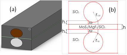
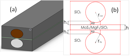
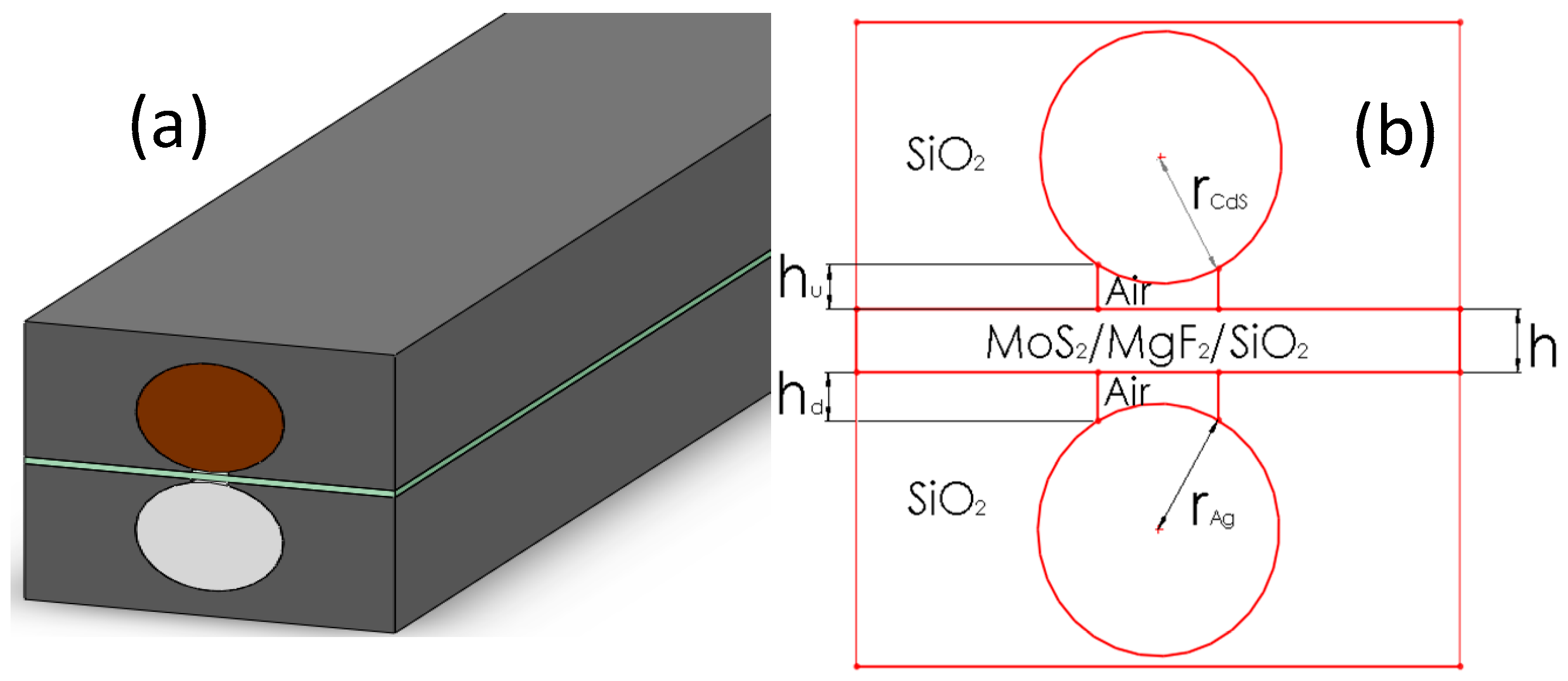
The structure presented in this paper is shown in Figure 1. The nanolaser includes a gain nanowire (the material is CdS, the radius is rCdS), spacer layer (MoS2, SiO2, and MgF2 have been selected as materials, the thickness is ‘h’), air gap (the thickness of upper air gap is hu, the thickness of lower air gap is hd), and metal nanowire (the material is silver, the radius is rAg). The longitudinal length of the structure is 10 μm. The geometry of the metal part and the gain part is cylindrical, which will lead to a good mode locality.
3. Simulation Analysis
The output wavelength of nanolaser is 489 nm [33] and the relative dielectric constants of Ag, CdS, MoS2, and SiO2 are −9.2 + 0.3i, 5.76, 19.7 + 7.7i, and 2.18 [34,35,36,37], respectively. This paper uses commercial COMSOL Multiphysics software based on the finite element method for the simulation calculation. The scattering boundary condition is chosen because the electromagnetic wave is almost completely transmitted under the scattering boundary condition. The plane wave is well absorbed and the incident wave is allowed to enter from any direction. This is one of the most commonly used boundary conditions to define the incident condition. More detailed mesh is selected to obtain more accurate results [38].
3.1. Discussion of Electric Field Distribution
The longitudinal electric field is discussed in this paper. Two-dimensional electric field distribution is shown as Figure 2a, and the electric field distribution of Ey at X = 0 is shown in Figure 2b. As can be seen from Figure 2, the energy is mainly distributed in the two air gaps between the CdS nanowire and the Ag nanowire, which is caused by the energy storage ability in the air gap. The electric field intensity around the CdS nanowire is greater than that of the Ag nanowire. This is because the surface plasma mode of the metal nanowire coupled with the high gain dielectric nanowire waveguide mode, which led to a considerable part of the electric field energy being localized in the gap around the CdS nanowire. This shows that at the junction of the two materials, the electric field will be enhanced and the degree of enhancement of different materials will be different.
3.1.1. Discussion on Electric Field Distribution of Different Materials
The electric field distribution of different materials is shown as Figure 3. The radii of the semiconductor nanowire and metallic nanowire are 80 nm, the thicknesses of materials MoS2, MgF2, and SiO2 are 5 nm, and the height of the air gaps is 5 nm. As can be seen from Figure 3, the material has no significant influence on the distribution of the electric field, but the electric field strength is seriously affected by the material. The nanolaser which takes MoS2 as the spacer layer has achieved the largest electric field intensity between the CdS nanowire and the Ag nanowire and the smallest electric field intensity in the spacer layer, while it has achieved the smallest electric field intensity between the CdS nanowire and the Ag nanowire and the largest electric field intensity in the spacer layer. In order to obtain a stronger electric field enhancement effect, taking MoS2 as the spacer layer is necessary.
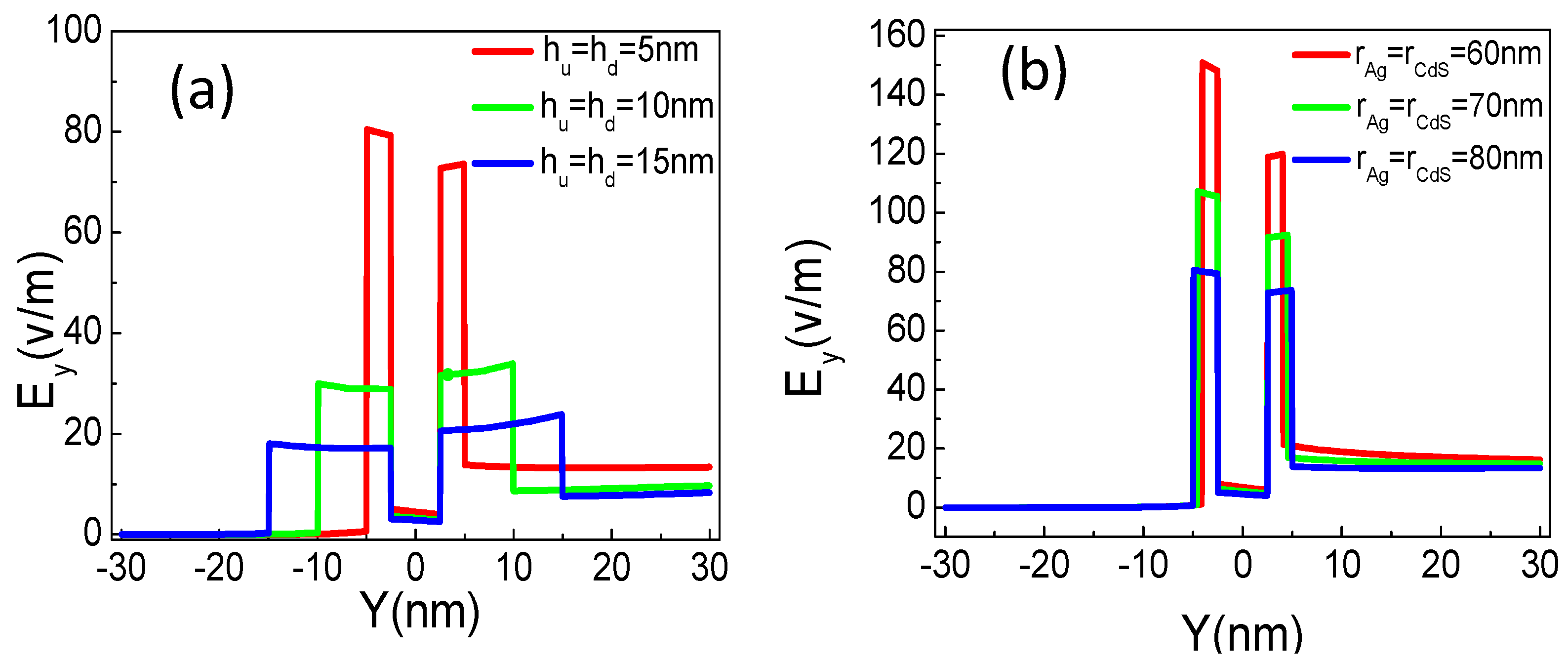
3.1.2. The Influence of Geometrical Structure on Electric Field Distribution
Figure 4 shows the electric field distribution of different geometries. Figure 4a is the electric field distribution of different air gap height. The radii of the semiconductor nanowire and metallic nanowire are 80 nm, and the height of the spacer layer is 5 nm. To analyze the influence of CdS nanowire and Ag nanowire, as shown in Figure 4b, the radii of the CdS nanowire and Ag nanowire have been changed. The height of the two air gaps is 5 nm, and the thickness of the intermediate spacer MoS2 is 5 nm. As can be seen from Figure 4, the higher the height of the air gap, the smaller the electric field intensity; the greater the radii of the CdS nanowire and Ag nanowire, the smaller the intensity of the electric field in the air gap. The main reason for this is energy conservation. When the height of the air gap is higher, the electric field intensity in the unit area of the air gap is lower. Thus, the energy is constant. When the radii of the CdS nanowire and Ag nanowire are greater, the curvature is smaller. Thus, the area of the air gap is increased, and the electric field intensity of the unit area is lower.
3.2. A Discussion of the Locality and Loss of Modes
The mode locality of the laser is expressed in a normalized mode area named Aeff/A0. The effective electric field area is defined as [39,40]:
The diffraction limit electric field area is defined as:
E represents the electric field intensity of the plasma wave and λ is the wavelength of the output light of the laser.
The mode loss is represented by the effective propagation loss named αeff [41]. In general, model locality and loss are contradictory. Many studies are trying to resolve this contradiction at present.
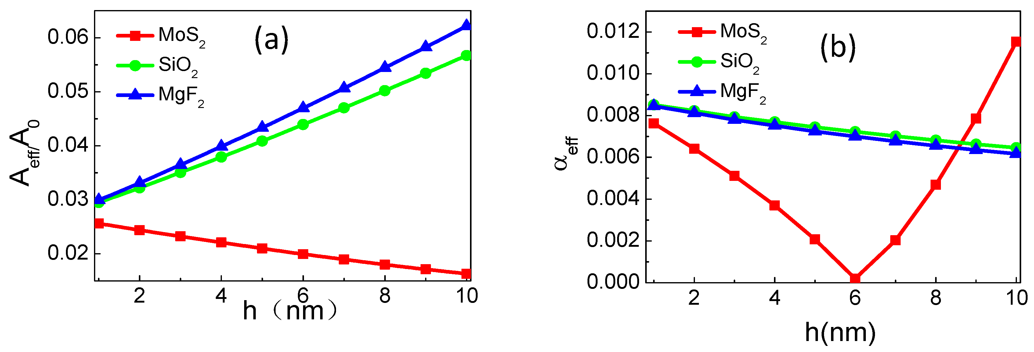
3.2.1. Discussion on Mode Locality of Different Materials
The normalized mode area (Figure 5a) and effective propagation loss (Figure 5b) for different materials are shown in Figure 5. The structure in Figure 5 is consistent with that in Figure 3. As can be seen from Figure 5, with the increase of the thickness of the space layer, the normalized mode area of the nanometer laser structure which chooses MoS2 as the space layer is smaller and smaller, and the effective propagation loss decreases first and then increases. However, the normalized mode area of nanolaser which selects MgF2 and SiO2 as the space layer is larger and larger, and the minimum value of normalized mode area is greater than the maximum value of normalized mode area of nanolaser using MoS2 as the space layer.
This difference is mainly because MoS2 is a transition metal sulfide, with a part of metallic properties that can enhance mode locality to some extent. MoS2 belongs to the hexagonal crystal system. It has a graphene-like structure, a large band gap [42,43], more excellent photoelectric properties than MgF2 and SiO2, high electron mobility, and good thermal stability, and it can store energy, reducing energy loss as a result.
3.2.2. Discussion on the Influence of Geometric Structure on the Localization and Loss of Modes
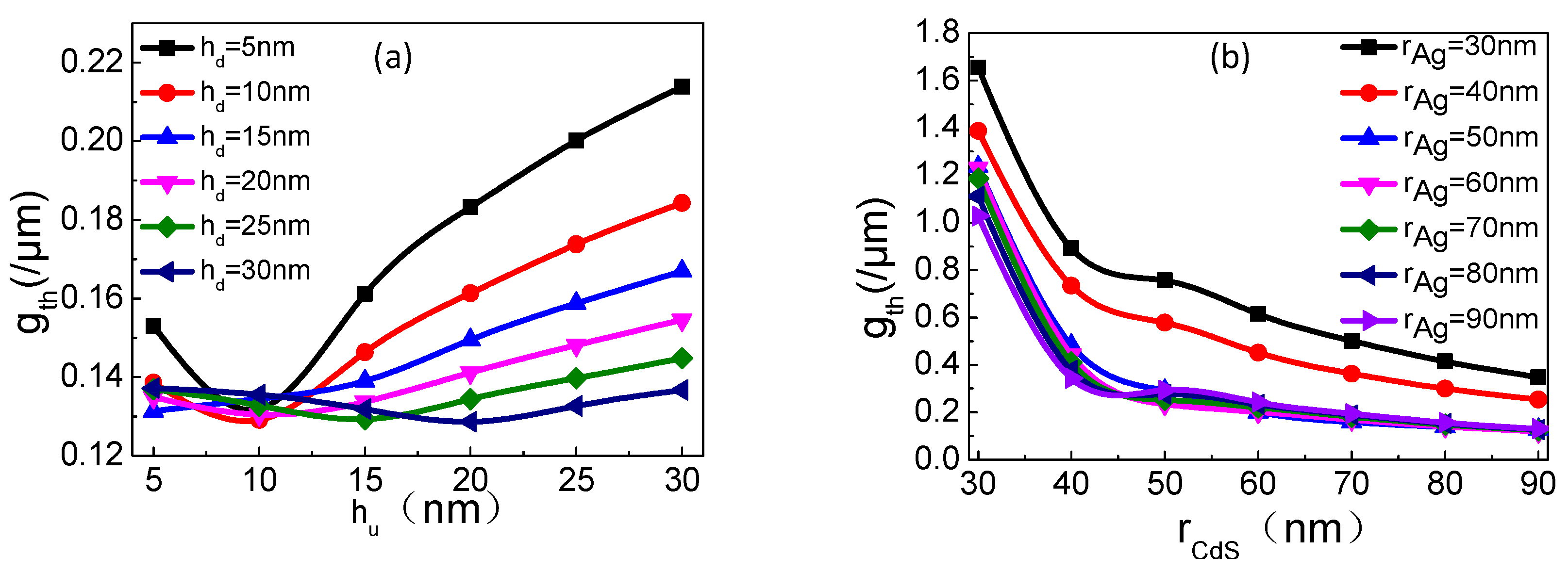
Figure 6a,c is the effects of the height of the air gap on the normalized mode area and the effective transmission loss. The radii of the Ag nanowires and CdS nanowires are fixed at 80 and 90 nm respectively in Figure 6a,c, and the spacer layer is fixed at 6 nm. Figure 6b,d is the effects of the CdS nanowire and Ag nanowire radius on the normalized mode area and effective transmission loss, in which the heights of the hu and hd are fixed and are both 10 nm. The structures in Figure 6a,c and Figure 4a are consistent. The structures in Figure 6b,d are consistent with those in Figure 4b, respectively. From Figure 6a,c, the normalized mode area increases as the height of the lower air gap increases, and the effective propagation loss decreases first and then increases, and the trend is upward. The minimums of the Aeff/A0 value and αeff are, respectively, 0.005 and 0.00013. With the increase of the height of the upper air gap, the normalized mode area and the effective propagation loss all decrease. With the increase of the Ag nanowire radius, the normalized mode area decreases gradually, and the effective propagation loss increases gradually. Through the comparison of the diagrams in Figure 6, it can be seen that the Ag nanowire and CdS nanowire play a more important role in the limited propagation loss. Among them, the Ag nanowire has the greatest impact. The height of the air groove has a greater influence on the normalized mode area, and the upper air groove has the greatest influence.
3.3. Discussion on Threshold
In the process of laser oscillation, there must be a certain gain in order to overcome the loss in the transmission process so as to realize and maintain the realization of laser oscillation. The minimum gain is the laser threshold. It is defined as [44,45,46]:
where k0 = 2π/λ. neff is effective refractive index, and αeff is effective propagation losses. They correspond to the imaginary part of the real part of the relative propagation constant of the plasma waveguide and the relative vector of the free space. nwire is the refractive index of the nanometer wire in the gain medium. Γ is a limiting factor used to characterize the field limiting power of the gain dielectric nanometer wire. It is defined as the ratio of the electric field energy in the nanometer wire to the total energy of the mode waveguide,
3.3.1. Discussion on Threshold of Different Materials
Figure 7 is the threshold of different materials, varying with the thickness of the space layer. Its structure is consistent with that of Figure 3. As can be seen from Figure 7, with the increase of the space layer thickness, the threshold of the nanolaser which uses MoS2 as the space layer decreases first and then increases. The minimum value is obtained when the thickness is 6 nm. However, the threshold of the nanolaser which takes MgF2 and SiO2 as the space layer is becoming smaller and smaller, but its minimum value is greater than the minimum value in which MoS2 is taken as the space layer. According to the conclusions of Figure 5, the nanolaser using MoS2 as space layer is not only better in locality, but also lower in threshold. Compared to that of MgF2 and SiO2, its comprehensive performance is the best.
3.3.2. Discussion on the Influence of Geometric Structure on Threshold
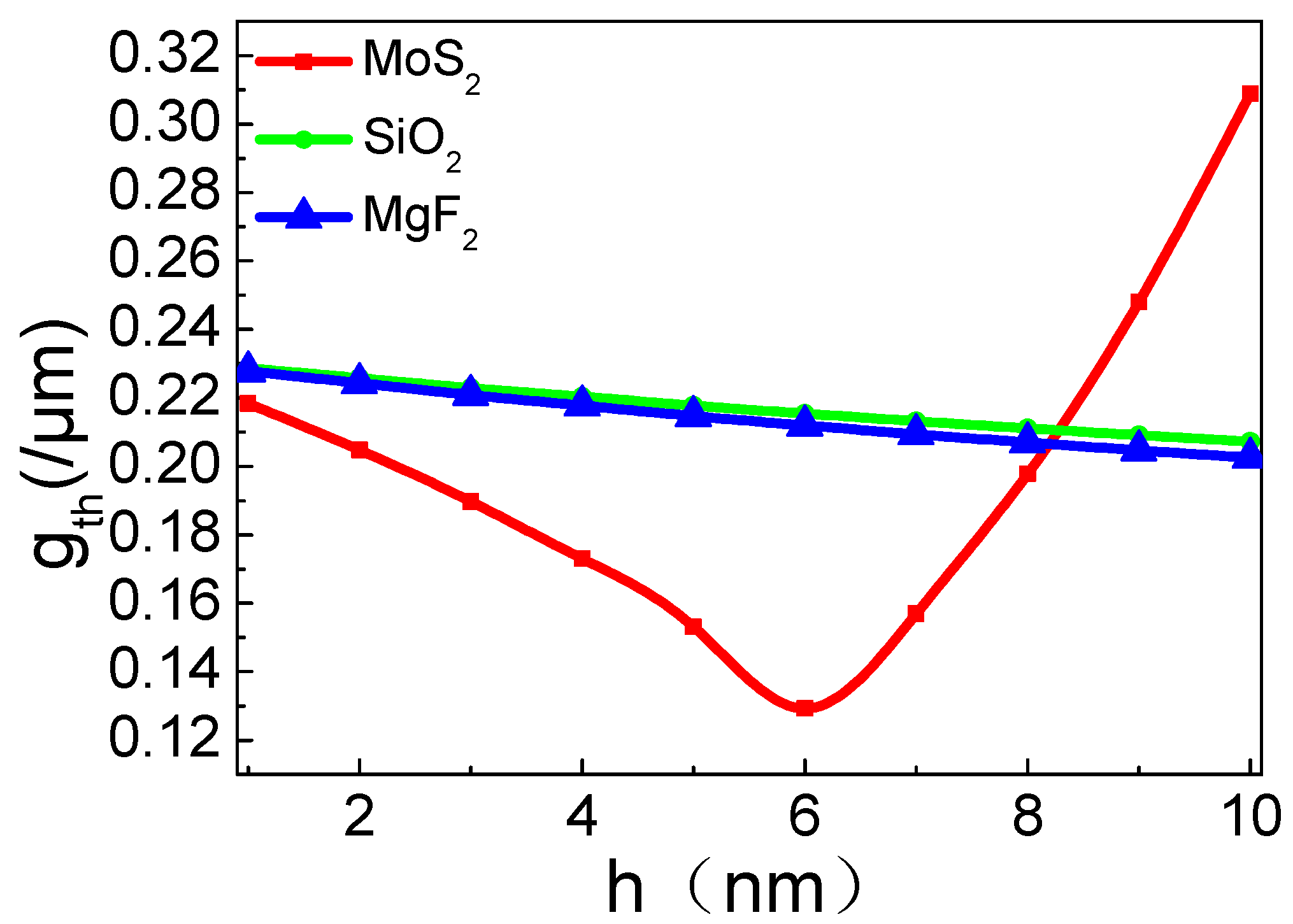
The threshold with different geometries is shown in Figure 8. The structures in Figure 8a,b are consistent with those shown in Figure 4a,b. As shown in Figure 8a, the threshold decreases as the height of the upper air gap increases. With the increase of the height of the lower air gap, the threshold decreases first and then increases, and the minimum threshold is 0.11 μm−1. As shown in Figure 8b, with the increase of the radius of the CdS nanowire and the Ag nanowire, the threshold shows a decreasing trend. When the radius is large, the threshold caused by the radius change is smaller. Comparing Figure 8a,b, we can see the influence of the height of the air gap on the mode localization is much smaller than that of the CdS nanowire and the Ag nanowire. Therefore, in order to obtain a lower threshold and smaller impact on other properties of the nanolaser, the radius of the CdS nanowire and the Ag nanowire should be changed preferentially.
In summary, in order to optimize the overall performance of the laser and to balance the contradiction between Aeff/A0 and αeff, the radius of the CdS nanowires and Ag nanowires are 90 nm and 80 nm respectively, the spacer layer is 6 nm, and the air gaps are all 10 nm, which means the threshold of the laser is lower while the normalized mode area is smaller. This structure can achieve deep subwavelength confinement and a low-lasing threshold.
4. Conclusions
In the paper, a new type nanolaser based on surface plasmon has been proposed. The electric field distribution, the mode property, and the threshold under different geometric shapes and parameters are investigated using the finite element method. The different influenced degree of each component is also analyzed. Under optimal parameters, effective propagation loss is only 0.00013, and the lasing threshold can be as low as 0.11 μm−1. This value is lower than the simulation results using spacers of MgF2 and SiO2 in Reference [41]. Simulation results reveal that this kind of nanolaser has a low threshold and high field confinement ability, the height of air gap makes a major contribution to the low threshold, and the field confinement ability of the nanolaser is mainly affected by the radius of the metal and gain medium. The structure and results provide theory and technique support to the field of new nanolaser design.
Author Contributions
L.W. and L.X. helped proceeding the simulation processes and data analysis; F.L. structured and planned the paper, and encouraged the team in paper writing; J.Z. and S.L. were also engaged in the simulation~processes.
Funding
This research was funded by the National Natural Science Foundation of China (Grant No. 11204222), the Natural Science Foundation of Hubei Province, China (Grant No. 2013CFB316, Grant No. 2014CFB793), and the Innovation Fund of School of Science, Wuhan Institute of Technology (No. CX2016106).
Acknowledgments
L.X. and L.F. would like to thank the support of the National Natural Science Foundation of China, the Natural Science Foundation of Hubei Province China, as well as the Innovation Fund of School of Science, Wuhan Institute of Technology.
Conflicts of Interest
The authors declare no conflict of interest.
References
- Rukhlenko, I.D.; Premaratne, M.; Agrawal, G.P. Guided plasmonic modes of anisotropic slot waveguides. Nanotechnology 2012, 23, 444006. [Google Scholar] [CrossRef] [PubMed]
- Han, Z.; Bozhevolnyi, S. Waveguiding with Surface Plasmon Polaritons. Rep. Prog. Phys. 2014, 76, 016402. [Google Scholar] [CrossRef] [PubMed]
- Sfez, T.; Descrovi, E.; Yu, L.; Brunazzo, D.; Quaglio, M.; Dominici, L.; Nakagawa, W.; Michelotti, F.; Giorgis, F.; Martin, O.J.F.; et al. Bloch surface waves in ultrathin waveguides: Near-field investigation of mode polarization and propagation. J. Opt. Soc. Am. B 2010, 27, 1617–1625. [Google Scholar] [CrossRef]
- Giorgis, F.; Descrovi, E.; Summonte, C.; Dominici, L.; Michelotti, F. Experimental determination of the sensitivity of bloch surface waves based sensors. Opt. Express 2010, 18, 8087–8093. [Google Scholar] [CrossRef] [PubMed]
- Paeder, V.; Musi, V.; Hvozdara, L.; Herminjard, S.; Herzig, H.P. Detection of protein aggregation with a bloch surface wave based sensor. Sens. Actuators B Chem. 2011, 157, 260–264. [Google Scholar] [CrossRef]
- Konopsky, V.N.; Alieva, E.V. A biosensor based on photonic crystal surface waves with an independent registration of the liquid refractive index. Biosens. Bioeletron. 2010, 25, 1212–1216. [Google Scholar] [CrossRef] [PubMed]
- Sinibaldi, A.; Rizzo, R.; Figliozzi, G.; Descrovi, E.; Danz, N.; Munzert, P. A full ellipsometric approach to optical sensing with bloch surface waves on photonic crystals. Opt. Express 2013, 21, 23331–23344. [Google Scholar] [CrossRef] [PubMed]
- Baryshev, A.V.; Merzlikin, A.M. Approach to visualization of and optical sensing by Bloch surface waves in noble or base metal-based plasmonic photonic crystal slabs. Appl. Opt. 2014, 53, 3142–3146. [Google Scholar] [CrossRef] [PubMed]
- Kong, W.; Wan, Y.; Zheng, Z.; Zhao, X.; Liu, Y.; Bian, Y. High-sensitivity sensing based on intensity-interrogated bloch surface wave sensors. Sens. Actuators B Chem. 2014, 193, 467–471. [Google Scholar] [CrossRef]
- Descrovi, E.; Frascella, F.; Sciacca, B.; Geobaldo, F.; Dominici, L.; Michelotti, F. Coupling of surface waves in highly defined one-dimensional porous silicon photonic crystals for gas sensing applications. Appl. Phys. Lett. 2007, 91, 1987. [Google Scholar] [CrossRef]
- Kong, W.; Wan, Y.; Ni, X.; Zhao, W.; Li, S.; Zheng, Z. Optimizing loss of the dielectric stack for Bloch-surface-wave sensors under different interrogation schemes. J. Mod. Opt. 2017, 64, 407–412. [Google Scholar] [CrossRef]
- Wan, Y.H.; Zheng, Z.; Kong, W.J.; Zhao, X.; Liu, J.S. Fiber-to-fiber optical switching based on gigantic bloch-surface-wave-induced goos–hanchen shifts. IEEE Photonics J. 2013, 5, 7200107. [Google Scholar]
- Olivieri, A.; Lisickaskrzek, E.; Northfield, H.; Liscidini, M.; Menotti, M.; Tait, N.; Fong, N.; Berini, P. Bloch long-range surface plasmon polaritons in metallic stripe waveguides. In CLEO: Science and Innovations; Optical Society of America: Washington, DC, USA, 2017. [Google Scholar]
- Fornasari, L.; Floris, F.; Patrini, M.; Canazza, G.; Guizzetti, G.; Comoretto, D. Fluorescence excitation enhancement by bloch surface wave in all-polymer one-dimensional photonic structure. Appl. Phys. Lett. 2014, 105, 117. [Google Scholar] [CrossRef]
- Toma, K.; Descrovi, E.; Toma, M.; Ballarini, M.; Mandracci, P.; Giorgis, F. Bloch surface wave-enhanced fluorescence biosensor. Biosens. Bioeletron. 2013, 43, 108–114. [Google Scholar] [CrossRef] [PubMed]
- Ballarini, M.; Frascella, F.; Michelotti, F.; Digregorio, G.; Rivolo, P.; Paeder, V.; Musi, V.; Giorgis, F.; Descrovi, E. Bloch surface waves-controlled emission of organic dyes grafted on a one-dimensional photonic crystal. Appl. Phys. Lett. 2011, 99, 144. [Google Scholar] [CrossRef]
- Fornasari, L.; Floris, F.; Patrini, M.; Comoretto, D.; Marabelli, F. Demonstration of fluorescence enhancement via bloch surface waves in all-polymer multilayer structures. Phys. Chem. Chem. Phys. 2016, 18, 14086–14093. [Google Scholar] [CrossRef] [PubMed]
- Wan, Y.H.; Zheng, Z.; Shi, X.G.; Bian, Y.S.; Liu, J.S. Hybrid plasmon waveguide leveraging Bloch surface polaritons for sub-wavelength confinement. Sci. China Technol. Sci. 2013, 56, 567–572. [Google Scholar] [CrossRef]
- Bartal, G.; Oulton, R.F.; Sorger, V.J.; Zhang, X. A Hybrid Plasmonic Waveguide for Subwavelength Confinement and Long Range Propagation. Nat. Photonics 2008, 2, 496. [Google Scholar]
- Ibarlucea, B.; Römhildt, L.; Zörgiebel, F.; Pregl, S.; Vahdatzadeh, M.; Weber, W.M.; Mikolajick, T.; Opitz, J.; Baraban, L.; Cuniberti, G. Gating Hysteresis as an Indicator for Silicon Nanowire FET Biosensors. Appl. Sci. 2018, 8, 950. [Google Scholar] [CrossRef]
- Xiang, Y.; Chen, J.; Zhang, D.; Wang, R.; Kuai, Y.; Lu, F.; Tang, X.; Wang, P.; Ming, H.; Rosenfeld, M.; et al. Manipulating Propagation Constants of Silver Nanowire Plasmonic Waveguide Modes Using a Dielectric Multilayer Substrate. Appl. Sci. 2018, 8, 144. [Google Scholar] [CrossRef]
- Wei, H.; Li, Z.P.; Tian, X.R.; Wang, Z.X.; Cong, F.Z.; Liu, N.; Zhang, S.P.; Nordlander, P.; Halas, N.J.; Xu, H.X. Quantum Dot-Based Local Field Imaging Reveals Plasmon-Based Interferometric Logic in Silver Nanowire Networks. Nano Lett. 2011, 11, 471–475. [Google Scholar] [CrossRef] [PubMed]
- Fang, Y.R.; Li, Z.P.; Huang, Y.Z.; Zhang, S.P.; Nordlander, P.; Halas, N.J.; Xu, H.X. Branched Silver Nanowires as Controllable Plasmon Routers. Nano Lett. 2010, 10, 1950–1954. [Google Scholar] [CrossRef] [PubMed]
- Shegai, T.; Miljkovic, V.D.; Bao, K.; Xu, H.X.; Nordlander, P.; Johansson, P.; Kall, M. Unidirectional Broadband Light Emission from Supported Plasmonic Nanowires. Nano Lett. 2011, 11, 706–711. [Google Scholar] [CrossRef] [PubMed]
- Pyayt, A.L.; Wiley, B.; Xia, Y.N.; Chen, A.T.; Dalton, L. Integration of Photonic and Silver Nanowire Plasmonic Waveguides. Nat. Nanotechnol. 2008, 3, 660–665. [Google Scholar] [CrossRef] [PubMed]
- Cao, L.N.; Nome, R.A.; Montgomery, J.M.; Gray, S.K.; Scherer, N.F. Controlling Plasmonic Wave Packets in Silver Nanowires. Nano Lett. 2010, 10, 3389–3394. [Google Scholar] [CrossRef] [PubMed]
- Goodfellow, K.M.; Beams, R.; Chakraborty, C.; Novotny, L.; Vamivakas, A.N. Integrated Nanophotonics Based on Nanowire Plasmons and Atomically-Thin Material. Optica 2014, 1, 149–152. [Google Scholar] [CrossRef]
- Wei, H.; Zhang, S.P.; Tian, X.R.; Xu, H.X. Highly Tunable Propagating Surface Plasmons on Supported Silver Nanowires. Proc. Natl. Acad. Sci. USA 2013, 110, 4494–4499. [Google Scholar] [CrossRef] [PubMed]
- Song, M.; Bouhelier, A.; Bramant, P.; Sharma, J.; Dujardin, E.; Zhang, D.; Colas-des-Francs, G. Imaging Symmetry-Selected Corner Plasmon Modes in Penta-Twinned Crystalline Ag Nanowires. ACS Nano 2011, 5, 5874–5880. [Google Scholar] [CrossRef] [PubMed]
- Drezet, A.; Hohenau, A.; Koller, D.; Stepanov, A.; Ditlbacher, H.; Steinberger, B.; Aussenegg, F.R.; Leitner, A.; Krenn, J.R. Leakage Radiation Microscopy of Surface Plasmon Polaritons. Mater. Sci. Eng. B 2008, 149, 220–229. [Google Scholar] [CrossRef]
- Yang, H.B.; Qiu, M.; Li, Q. Identification and Control of Multiple Leaky Plasmon Modes in Silver Nanowires. Laser Photonics Rev. 2016, 10, 278–286. [Google Scholar] [CrossRef]
- Wang, Z.X.; Wei, H.; Pan, D.; Xu, H.X. Controlling the Radiation Direction of Propagating Surface Plasmons on Silver Nanowires. Laser Photonics Rev. 2014, 8, 596–601. [Google Scholar] [CrossRef]
- Jia, Z.L.; Wei, H.; Pan, D.; Xu, H.X. Direction-Resolved Radiation from Polarization-Controlled Surface Plasmon Modes on Silver Nanowire Antennas. Nanoscale 2016, 8, 20118–20124. [Google Scholar] [CrossRef] [PubMed]
- Zhang, D.G.; Xiang, Y.F.; Chen, J.X.; Cheng, J.J.; Zhu, L.F.; Wang, R.X.; Zou, G.; Wang, P.; Ming, H.; Rosenfeld, M.; et al. Extending the Propagation Distance of a Silver Nanowire Plasmonic Waveguide with a Dielectric Multilayer Substrate. Nano Lett. 2018, 18, 1152–1158. [Google Scholar] [CrossRef] [PubMed] [Green Version]
- Zhan, Q.W. Cylindrical Vector Beams: From Mathematical Concepts to Applications. Adv. Opt. Photonics 2009, 1, 1–57. [Google Scholar] [CrossRef]
- Zhang, S.P.; Xu, H.X. Optimizing Substrate-Mediated Plasmon Coupling toward High-Performance Plasmonic Nanowire Waveguides. ACS Nano 2012, 6, 8128–8135. [Google Scholar] [CrossRef] [PubMed]
- Palik, E.D.; Ghosh, G. Handbook of Optical Constants of Solids; Academic Press: Cambridge, MA, USA, 1998. [Google Scholar]
- Lv, H. Hybrid Plasmonic Waveguides for Low Threshold Nanolasers; Beijing University of Posts and Telecommunications Press: Beijing, China, 2015. [Google Scholar]
- Joannopoulos, J.D.; Johnson, S.G.; Winn, J.N.; Meade, R.D. Photonic Crystals: Molding the Flow of Light; Princeton University Press: Princeton, NJ, USA, 2008. [Google Scholar]
- Gerard, D.; Wenger, J.; Devilez, A.; Gachet, D.; Stout, B.; Bonod, N.; Popov, E.; Rigneault, H. Strong Electromagnetic Confinement near Dielectric Microspheres to Enhance Single-Molecule Fluorescence. Opt. Express 2008, 16, 15297–15303. [Google Scholar] [CrossRef] [PubMed]
- Lv, H.; Liu, Y.; Yu, Z. Hybrid plasmonic waveguides for low-threshold nanolaser applications. Chin. Opt. Lett. 2014, 12, 103–106. [Google Scholar]
- Torbatian, Z.; Asgari, R. Plasmonic Physics of 2D Crystalline Materials. Appl. Sci. 2018, 8, 238. [Google Scholar] [CrossRef]
- Lerario, G.; Ballarini, D.; Dominici, L.; Fieramosca, A.; Cannavale, A.; Holwill, M.; Kozikov, A.; Novoselov, K.S.; Gigli, G. Bloch Surface Waves for MoS2 Emission Coupling and Polariton Systems. Appl. Sci. 2017, 7, 1217. [Google Scholar] [CrossRef]
- Estrada, L.C.; Martinez, O.E.; Brunstein, M.; Bouchoule, S.; Le-Gratiet, L.; Talneau, A.; Sagnes, I.; Monnier, P.; Levenson, J.A.; Yacomotti, A.M. Small volume Excitation of Dye Fluorescence on a 2D Photonic Crystal Surface. Opt. Express 2010, 18, 3693–3699. [Google Scholar] [CrossRef] [PubMed]
- Wenger, J.; Gerard, D.; Aouani, H.; Rigneault, H.; Lowder, B.; Blair, S.; Devaux, E.; Ebbesen, T.W. Nanoaperture-Enhanced Singla-to-Noise Ratio in Fluorescence Correlation Spectroscopy. Anal. Chem. 2009, 81, 834–839. [Google Scholar] [CrossRef] [PubMed]
- Estrada, L.C.; Aramendia, P.F.; Martinez, O.E. 10,000 times Reduction for Fluorescence Correlation Spectroscopy Using Nano-Antenna. Opt. Express 2008, 16, 20597–20602. [Google Scholar] [CrossRef] [PubMed]
Figure 1.
(a) The block diagrams and (b) the section plan of nanolaser.

Figure 2.
(a) The electric field distribution of nanolaser; (b) The intensity distribution of Ey.
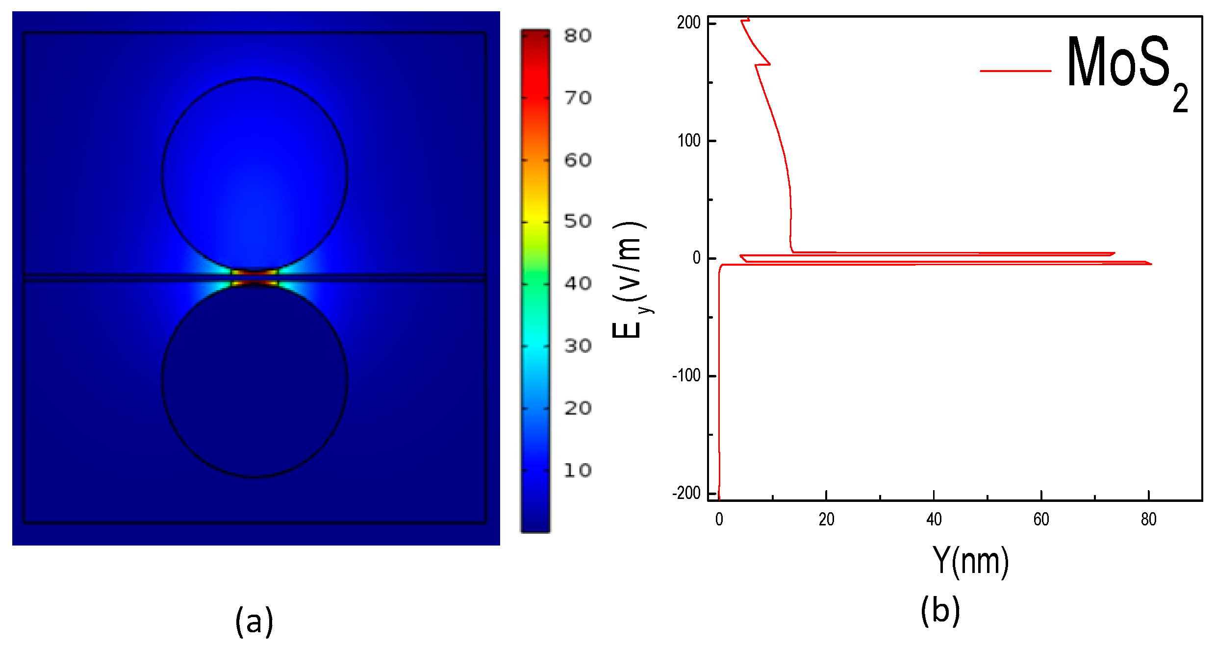
Figure 3.
The electric field distribution with different materials.
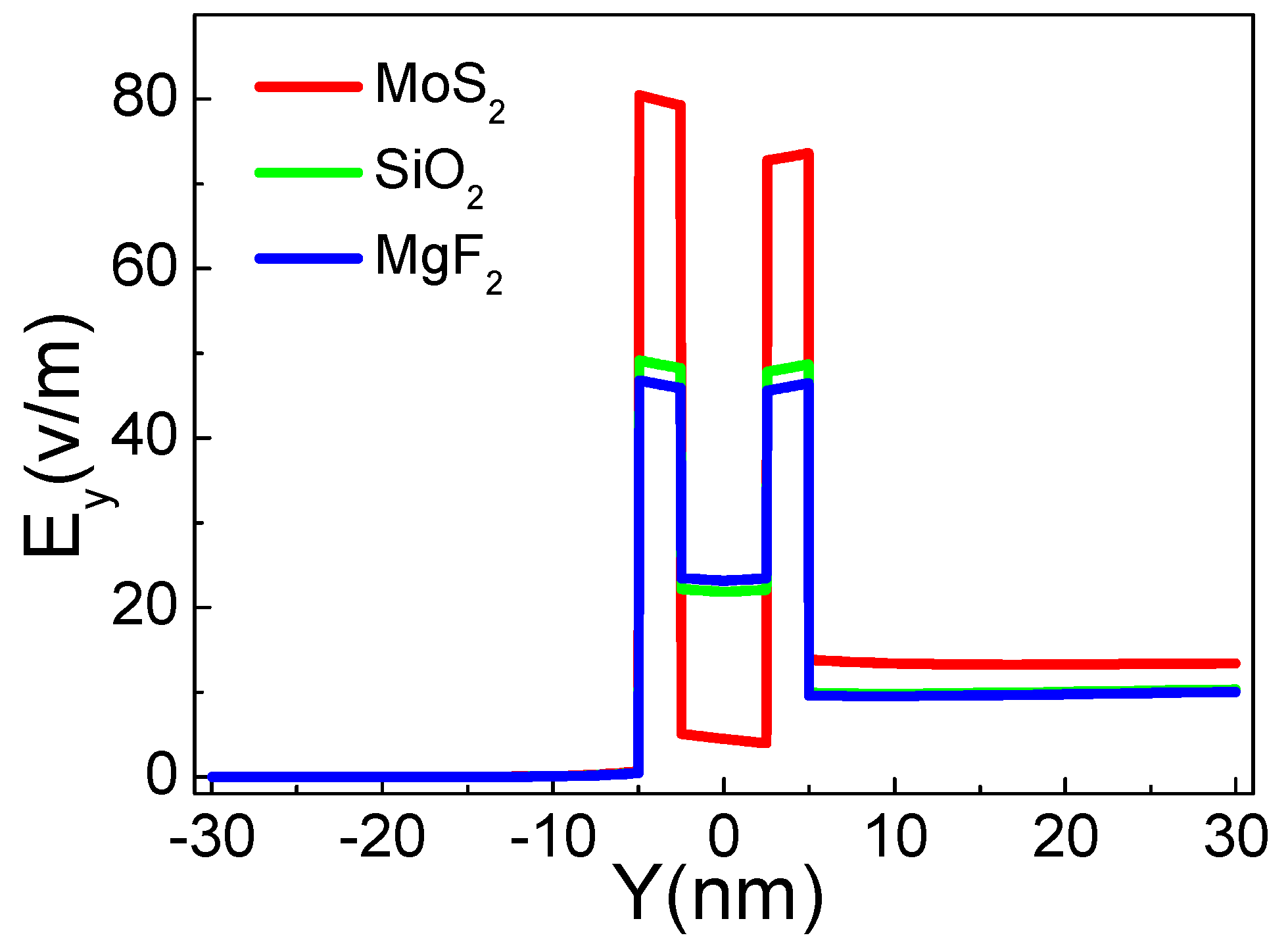
Figure 4.
The electric field distribution of nanolaser versus (a) the height of the air gap, (b) the radius of CdS and Ag.
Figure 4.
The electric field distribution of nanolaser versus (a) the height of the air gap, (b) the radius of CdS and Ag.

Figure 5.
The normalized mode area and loss with different materials and the thickness of the space layer (a) the normalized mode area (b) the propagation loss.
Figure 5.
The normalized mode area and loss with different materials and the thickness of the space layer (a) the normalized mode area (b) the propagation loss.

Figure 6.
The normalized mode area and loss of nanolaser versus (a,c) the height of air gap, (b,d) the radius of CdS and Ag.
Figure 6.
The normalized mode area and loss of nanolaser versus (a,c) the height of air gap, (b,d) the radius of CdS and Ag.
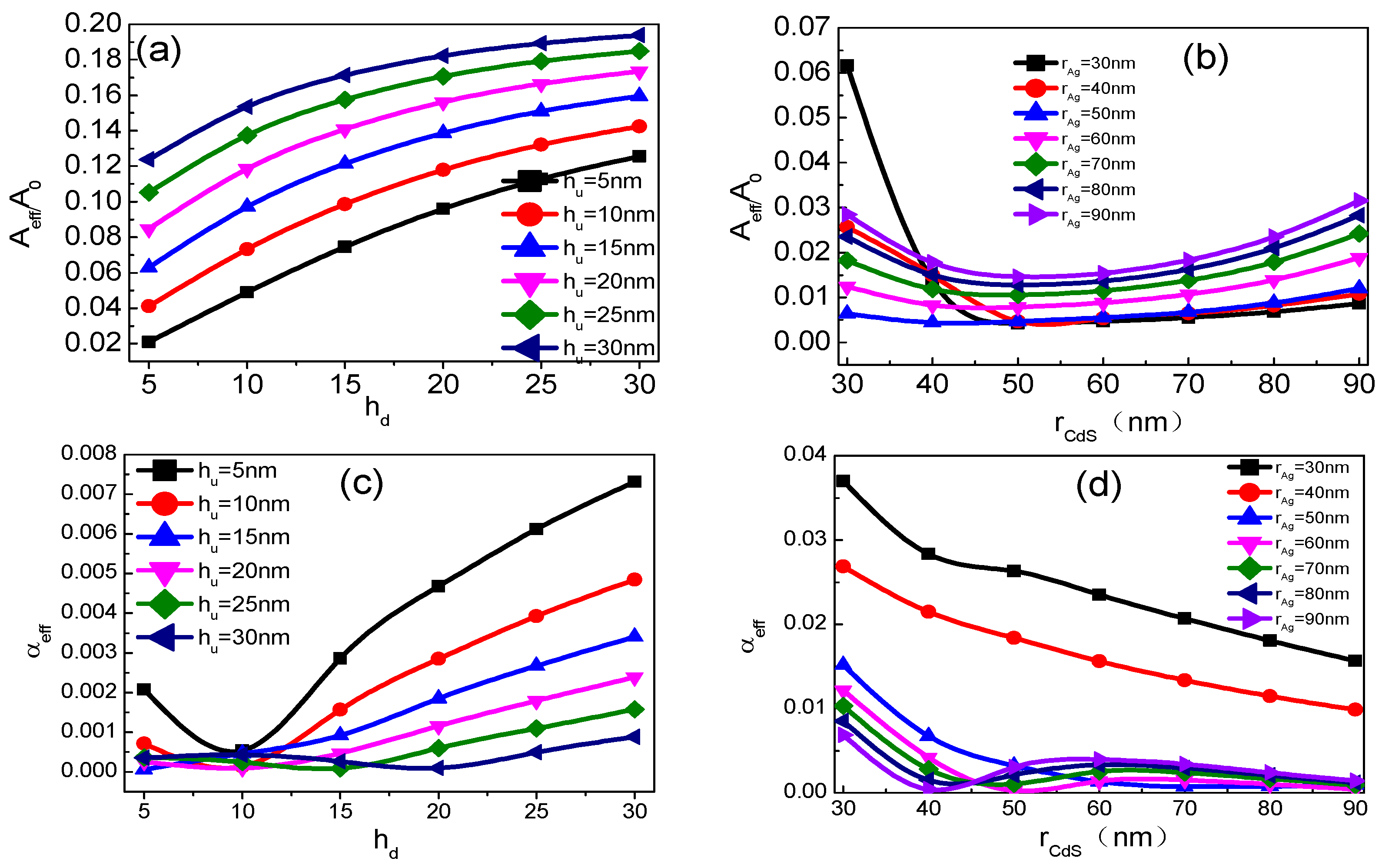
Figure 7.
The threshold with different materials.

Figure 8.
The threshold of nanolaser versus (a) the height of air gap, (b) the radius of CdS and Ag.
Figure 8.
The threshold of nanolaser versus (a) the height of air gap, (b) the radius of CdS and Ag.

© 2018 by the authors. Licensee MDPI, Basel, Switzerland. This article is an open access article distributed under the terms and conditions of the Creative Commons Attribution (CC BY) license (http://creativecommons.org/licenses/by/4.0/).
Share and Cite
MDPI and ACS Style
Xu, L.; Li, F.; Wei, L.; Zhou, J.; Liu, S. Design of Surface Plasmon Nanolaser Based on MoS2. Appl. Sci. 2018, 8, 2110. https://doi.org/10.3390/app8112110
AMA Style
Xu L, Li F, Wei L, Zhou J, Liu S. Design of Surface Plasmon Nanolaser Based on MoS2. Applied Sciences. 2018; 8(11):2110. https://doi.org/10.3390/app8112110
Chicago/Turabian StyleXu, Litu, Fang Li, Lai Wei, Jianxin Zhou, and Shuai Liu. 2018. "Design of Surface Plasmon Nanolaser Based on MoS2" Applied Sciences 8, no. 11: 2110. https://doi.org/10.3390/app8112110
Note that from the first issue of 2016, this journal uses article numbers instead of page numbers. See further details here.