Article

A Modified Interposer Fabrication Process by Copper Nano-Pillars Filled in Anodic Aluminum Oxide Film for 3D Electronic Package

State Key Laboratory of Advanced Welding and Joining, Harbin Institute of Technology, Harbin 150001, China
*
Author to whom correspondence should be addressed.
Appl. Sci. 2018, 8(11), 2188; https://doi.org/10.3390/app8112188
Submission received: 24 October 2018 / Revised: 4 November 2018 / Accepted: 4 November 2018 / Published: 8 November 2018
(This article belongs to the Special Issue Selected Papers from the NMJ2018)

Abstract

:
Though copper nano-pillars (CNPs) filled in anodic aluminum oxide (AAO) film has been developed for many years, the high pore-filling percentage in AAO is still a bottleneck. We have demonstrated a new electrodeposition method to fill CNPs in AAO without the seed layer which is required in the traditional electrodeposition process. CNPs with uniform heights were obtained and the pore-filling percentage reached up to 97.5%. Low current density is beneficial for the high pore-filling percentage due to the uniform growing rate in different nanoscale pores. The high temperature increased the diffusion velocity of ions and enhanced the pore filling percentage but also corroded the AAO film simultaneously. Results showed that CNPs grains with <220> orientation were fabricated. Electrodeposition with low electric current could contribute to the forming of CNPs with (220) preferred orientation due to the promotion of dehydration reduction processes. The thermal conductivities of Cu-AAO interposers reaches 92.34 W/(m·K) and 3.19 W/(m·K) in vertical and horizontal directions, respectively.

1. Introduction

The change from two-dimensional integrated circuits (2D ICs) to 3D ICs is a trend in the electronics industry to break through the limits of very-large-scale integration circuits (VLSI) [1,2]. The interposer structure, which is a crucial part in 3D ICs, has been served as a substrate that can provide a rigid insulating layer between stacked chips and can provide electrical connectivity between layers through the embedded vertical vias [3].
Though silicon with through silicon vias (TSVs) has served as the interposer in 3D ICs for many years [4,5,6], it is far from popular in the industry because of its high cost during the fabrication process which involves deep reactive ion etching (DRIE), chemical vapor deposition (CVD), physical vapor deposition (PVD), etc. [7]. In addition, the coefficient of thermal expansion (CTE) mismatch among silicon (2.5 ppm/K), silicon dioxide (0.6 ppm/K), and copper (17.5 ppm/K) also will bring many serious reliability problems, such as cracks and delamination. Recently, glass with superior insulating property and low cost has been introduced as a replacement for silicon [8]. Unfortunately, the formation of the vias in glass with a diameter of less than 50 μm was proved to be very difficult due to the frangibility of glass. Anodic aluminum oxide (AAO) films can provide natural close-packed parallel cylindrical nano-pores [9,10,11], thus the drilling process and other high-cost processes for via pores can be avoided.
To endow the interposer with electrical conductivity at special areas, the AAO can be filled with copper nano-pillars (CNPs) using the electrodeposition process. The conventional electrodeposition process needs to prefabricate high-quality seed layers on the interposer surface, which involves complicated fabrication processes [12,13,14,15], such as the sputtering process, as indicated in Figure 1a. Furthermore, the high pore-filling percentage in AAO is still a bottleneck [16]. The effects of technical parameters (current density and temperature) on the pore-filling percentage need to be systematically investigated.
In this study, indium tin oxide (ITO) conductive glass, an ideal material with high conductivity and extremely flat surface was used as the conductive substrate during the electrodeposition process. As shown in Figure 1b, the AAO film was tightly fixed onto the ITO glass surface using insulating sealant and insulated adhesive tape. The ITO glass served as a frame and an electrode for the AAO film during the subsequent electrodeposition process and the uniform nano-pillars were obtained in an AAO template. After deposition, the ITO glass can be easily removed from the AAO structure. To achieve a high pore-filling percentage, electrodeposition parameters (current density, temperature) of Cu nano-pillars were investigated.

2. Materials and Methods

AAO film (Figure 2) with an average thickness of 55 μm, interpore diameter of 70 nm, and interpore center distance of 125 nm was used in this study. AAO film was fixed onto ITO conductive glass with insulating sealant and insulating adhesive tape. Firstly, the AAO film and ITO glass were fixed together by insulating sealant, to ensure the sealing between AAO film and ITO glass. Subsequently, the other areas of the ITO glass were covered with adhesive tape to prevent the unwanted Cu deposition. The AAO film was set as a cathode and copper plate was employed as an anode. The anode copper plate was prepared with 1 mol/L H2SO4 solution to remove the surface oxides. An electrolyte mixture of 1.5 mol/L CuSO4·5H2O and 1.5 mol/L H2SO4 aqueous was used.
Electrodeposition experiments were carried out by a direct current (DC) power supplier (ZHAO XIN, Shenzhen, China). SEM images were collected using Merlin Compact (ZEISS, Oberkochen, Germany) with an acceleration voltage of 20 kV. Crystalline structure was characterized by X-ray diffractometer (BRUKER AXS GMBH, Rheinstetten, Germany) using a Rigaku D/max-γB diffractometer with a Cu Kα emission source and wavelength of λ = 1.5418 Å, a scanning speed of 5°/min and a step of 0.02°. The electrochemical testing was accomplished by electrochemical workstation (CHENHUA, Shanghai, China). Hg(s)/Hg2SO4(aq)/SO42−(aq) was set as reference electrode. The density of the Cu-AAO interposer was measured by drainage method. Heat capacity was measured by a differential scanning calorimeter (NETZSCH, Bavaria, Germany), and the thermal diffusion coefficient was collected by a laser thermal conducting instrument (NETZSCH, Bavaria, Germany). The pore-filling percentage was counted by the number of filled pores divided by the number of all pores. For the convenience of the pore-filling percentage calculation, the samples were polished to remove the excess copper bulks on top to reveal the filled Cu pillars. Under each parameter, three samples were selected for the pore-filling percentage calculation.

3. Results and Discussion

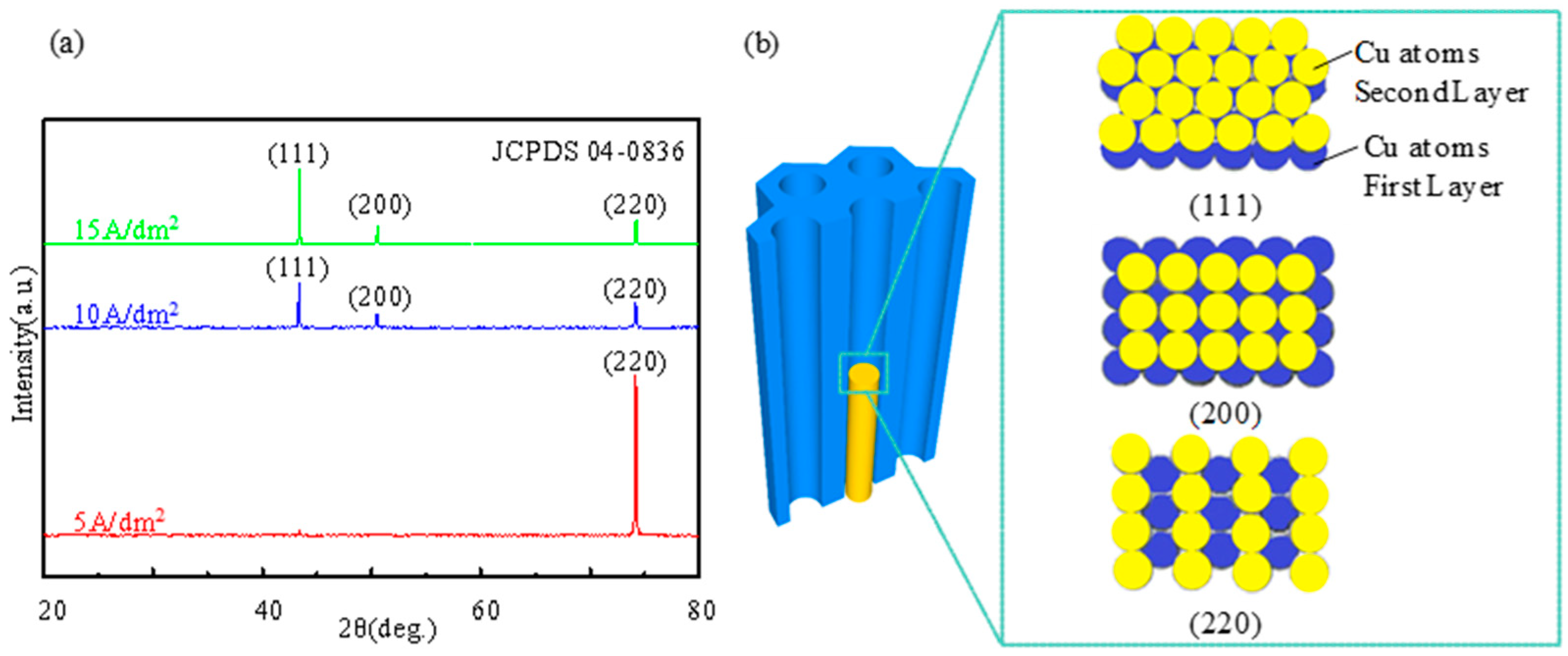
3.1. Effect of Parameters on Pore-Filling Percentage

The experiment was carried out under different current densities (5 A/dm2, 10 A/dm2, 15 A/dm2) at 40 °C. Figure 3a shows the pore-filling results under 5 A/dm2, nearly all pores had been filled and the pore-filling percentage had reached 97.5%. When current density was 10 A/dm2, the pore-filling percentage was decreased to 61.8%, as shown in Figure 3b. When the current density was 15 A/dm2, only a few pores were filled, and the pore-filling percentage decreased to 35.8% (Figure 3c). The curve of pore-filling percentage versus the current densities is displayed in Figure 3d. These results revealed that lower current density is beneficial for higher pore-filling percentages.
High current density will bring a higher driving force, which increases the movement speed of copper ions and enlarge the uneven movement of copper ions, resulting in different growing rates in different pores [17,18,19]. A uniform growing rate of CNPs in different pores is required for high pore-filling percentages. The mechanism is shown in Figure 4a, some nano-pillars with high growing rates firstly reached the AAO film surface and then spread out onto the surrounding area. After the continuous copper bulks formed on the top surface, the pillar filling process in these pores under the copper bulks stopped, as indicated in Figure 4b. The blocking of pores and impeding of pillars were caused by the small copper bulks. The percentage of blocked pores (PBP) at high current density was counted by Equation (1) using Figure 4c:
PBP = Nb/Na = (Sb × p)/(Sa × p) = Sb/Sa
In which Nb and Na are the number of blocked pores and the number of all pores, respectively. Sb and Sa are the area of AAO film covered by copper bulk and the whole area of AAO film, respectively. p is the area percentage of pores. The area was counted by pixels in the Photoshop software. The percentage of blocked pores was 41.2% for the samples fabricated under 40 °C and the current density of 15 A/cm2 at 4 h. With a lower current density, a uniform growth happened and the nano-pillar in each pore grew sufficiently, resulting in a high pore-filling percentage, as shown in Figure 4e–f.
To investigate the effect of temperature on the nano-pillar growth behavior, the current density is fixed at 10 A/dm2. Figure 5 shows the AAO film surfaces after electrodeposition process under different deposition temperatures (20 °C, 40 °C, 60 °C). Figure 5a shows that a low pore-filling percentage of 40.2% was obtained at 20 °C. When the electrodeposition temperature increased up to 40 °C, more pores were filled, and the pore-filling reached 61.8%. Lastly, the pore-filling percentage reached up to 89.8% under 60 °C. The relationship between the pore-filling percentage and temperature is shown in Figure 5d. The pore-filling percentage increased with the electrodeposition temperature.
The effect of electrodeposition temperature can be explained by diffusion. Equation (2) shows the relationship between diffusion coefficient and temperature:
D = D0 ∗ exp((−Q)/RT)
where D is diffusion coefficient, D0 is diffusion constant, Q is activation energy, R is gas constant, and T is absolute temperature. It can be seen that the diffusion velocity is positively correlated with the temperature. The Cu2+ needs to diffuse from the electrolyte to the bottom of the pores. Cu2+ at high temperature would have a high diffusion velocity and enter the nanoscale pores more easily than that at low temperature, leading to a high pore-filling percentage.
AAO film provided the dielectric performance and supporting frame for vertical interconnection, and its integrity is very important. Although high pore-filling percentage (Figure 5c) could be observed at 60 °C, serious corrosion of the AAO film was also observed at 60 °C. As shown in Figure 5e, the dissolution of AAO films in some area resulted in the exposure of CNPs. The dissolution was caused by the excessive hydrogen ions. It was mentioned above that sulfuric acid was used in the electrolyte and thus lots of hydrogen ions were contained in the electrolyte and the chemical reaction between acid and metallic oxide would occur with the following way:
6H+ + Al2O3 → 2Al3+ + 3H2O
At low temperature, the chemical reaction rate is slow, which has a small influence on the corrosion of AAO. As the temperature increases, the chemical reaction rate increases gradually. Hence, the corrosion of AAO is serious at high temperature. It is necessary to balance the conflict between the damage and the high pore-filling percentage. In summary, the electrodeposition temperature of 40 °C was expected to be optimum, with the electrodeposition current density of 5 A/dm2 in this work.

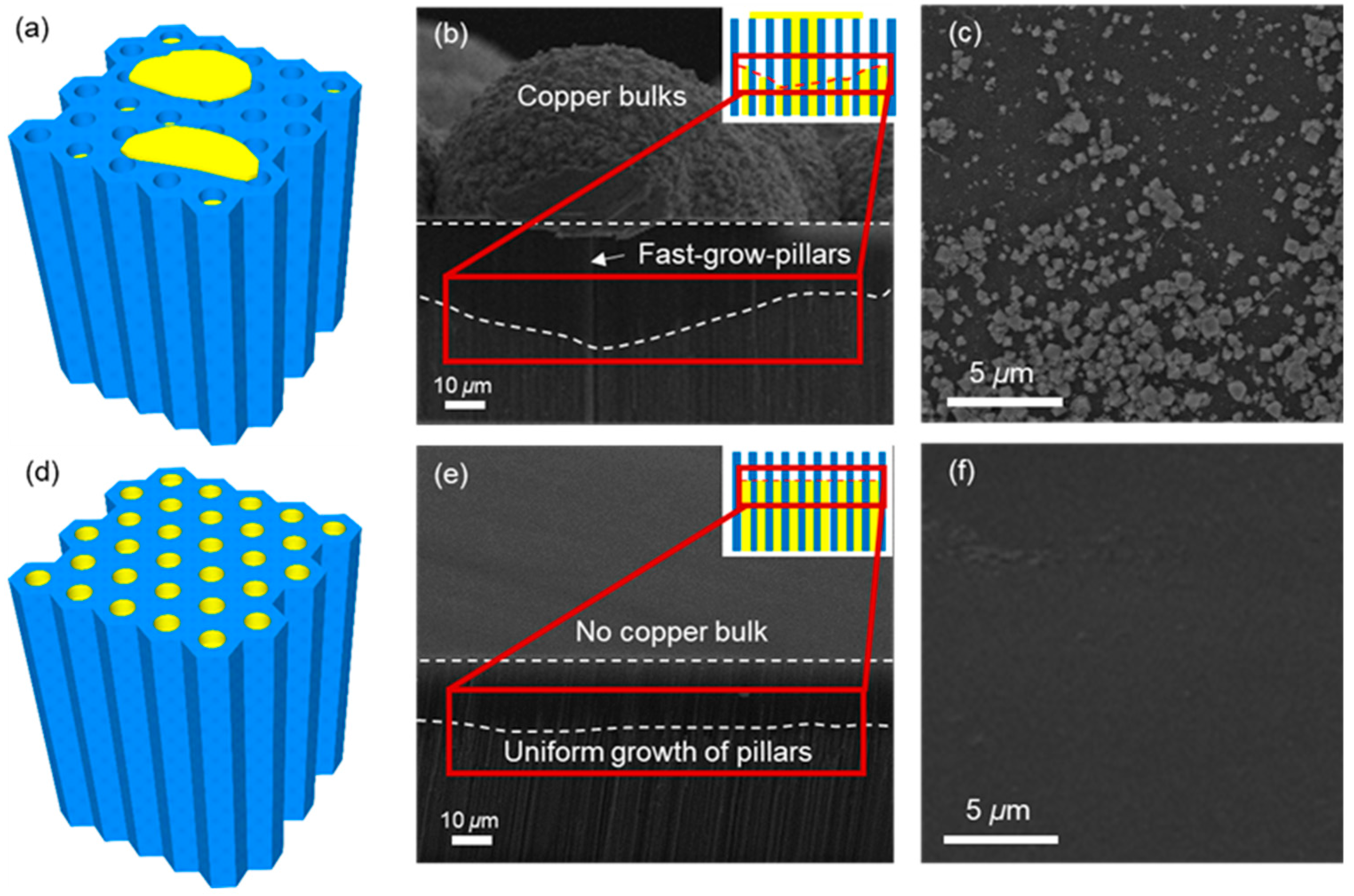
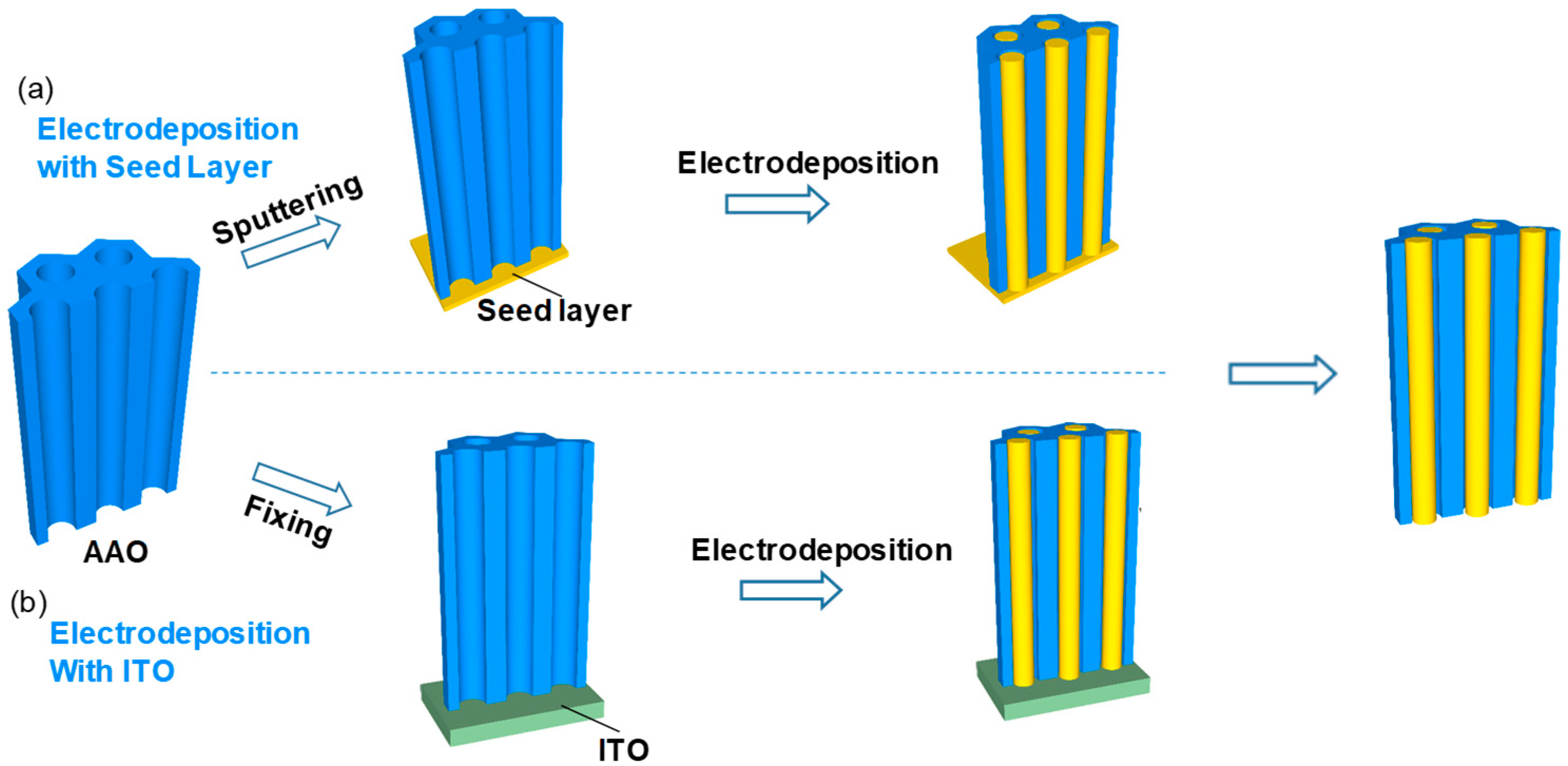
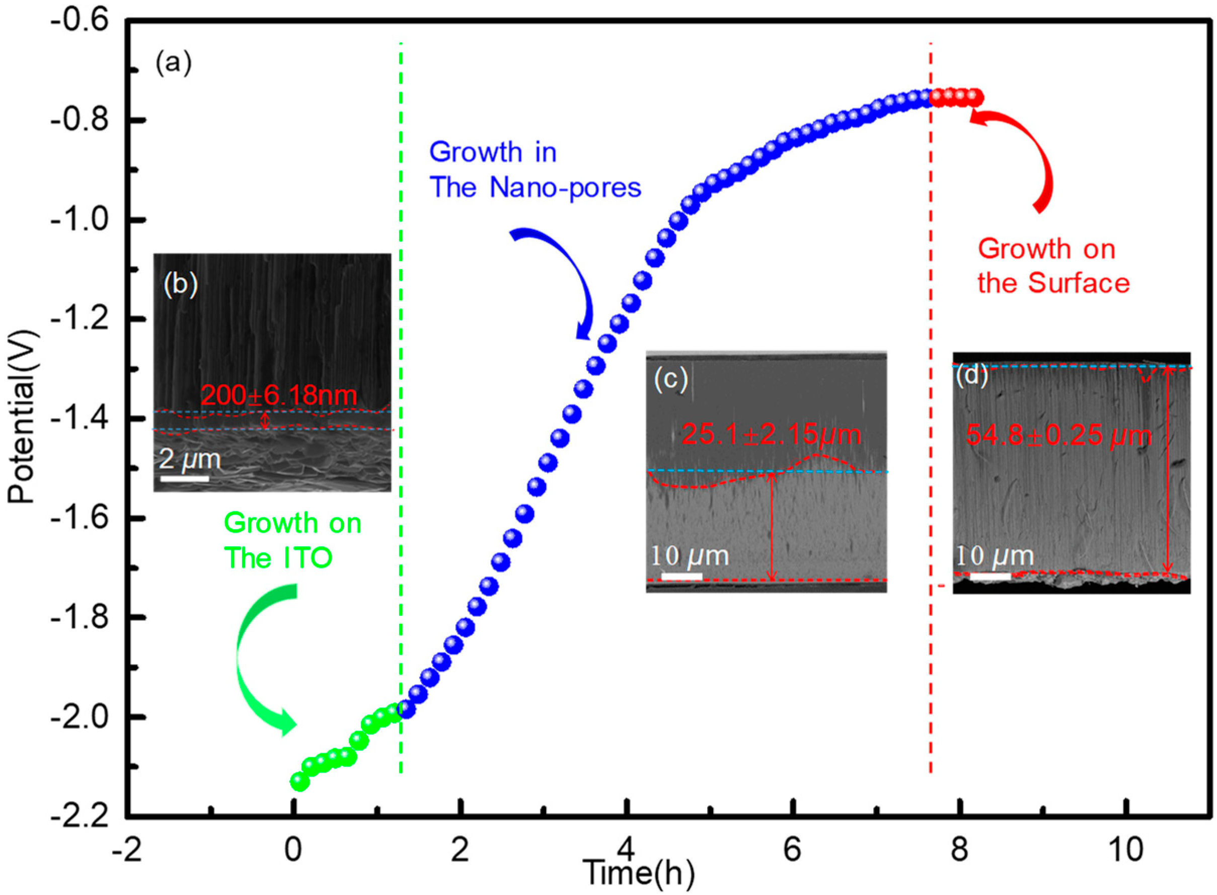
3.2. Growth of CNPs on ITO

The growth process of CNPs on ITO was investigated by chronopotentiometry (V-t characteristic curve) experiment with electrodeposition parameters of 5 A/dm2 and 40 °C. The obtained potential-time curve (Figure 6a) can be divided into three stages during the growth process. At the beginning, a thin copper layer with a thickness of ~200 nm was generated in the tiny gap between the AAO film and the ITO glass, as shown in Figure 6b. The gap distance between AAO film and ITO glass slightly changed in each experiment. Thus, the time for the first stage will have a tiny change. However, the varying distance does not affect subsequent stages. The first section of growth is to fill the gap and obtain a uniform copper layer, which will be the seed layer for the subsequent growth of the copper pillars. As long as the gap is filled, and a uniform seed layer is formed, copper nano-pillars could grow uniformly on this basis. The potential was extremely negative, indicating the difficulties for electrodeposition on ITO glass [20,21]. It was believed that the surface of ITO glass (with the surface roughness of 0.312 nm) is relatively smooth and it is difficult to find nucleation sites. Hence, great negative potential was necessary to provide the drive force for copper atoms diffusion onto ITO glass. With the continuous deposition of copper atoms, a thin copper layer covered the ITO glass surface. The deposition on the copper layer was easier and the potential increased. After filling of gap between AAO film and ITO glass, Cu2+ accumulated in the nano-pores and CNPs was formed (Figure 6c). It was difficult for Cu2+ to pass through the nano-pores of the template, so the potential was still relatively negative to provide the drive force. As the heights of CNPs increased, the diffusion distance required for Cu2+ to the deposition surface was shorter and the potential increased. At the last period, the potential is almost constant, indicating that the growth of CNPs finished and copper atoms deposited on the surface of the AAO film (Figure 6d).
The electrodeposition process can be divided into four steps [22]. Firstly, the hydrated copper cations diffused from the electrolyte onto the cathode surface. Secondly, the hydrated copper cations transformed into copper atoms by dehydration and reduction. Thirdly, the copper atoms deposited onto the cathode surface. Finally, the deposited copper atoms incorporated into the ionic metal lattices and started to crystallize.

3.3. Performance of Cu-AAO Interposer

According to the X-ray diffraction (XRD) analysis results, only the (220) crystal plane could be observed when the electrodeposition current density was 5 A/dm2 (as shown in Figure 7a), which indicated that the CNPs have formed a single crystal structure, and <220> is the preferred crystal orientation. When the current density increased to 10 A/dm2 and 15 A/dm2, the crystal planes with crystal planes of (111), (200), and (220) were observed (as shown in Figure 7b), which revealed the CNPs are the polycrystalline structure. In fact, CNPs with a single-crystal is beneficial to fabricating the unidirectional microbumps in the subsequent Cu/Sn bumping process, which can suppress the vacancy formation and improve the interconnection reliability [23].
It is reported that lower current density resulted in lower overpotential, and further resulted in lower nucleation rates. The observations in this study are consist with the references [12,18]. During the crystallization process, there are two ways for crystal formation to occur. One is the continuing growth on the preexisting crystal nuclei and the other is the formation of new grains [21,22,23,24,25,26]. According to the above-mentioned discussion, low current density and low overpotential will suppress the nucleation rate. Therefore, the copper pillars will prefer to grow along initial crystal orientation and newly formed grains will be greatly suppressed.
Preferred forming of the (220) crystal plane was caused by the dehydration reduction process. During the growing process of CNPs, copper ions in electrolyte need to obtain electrons to form copper atoms. Therefore, the CNPs will choose the crystal structure that is most favorable for receiving electrons [22]. As the copper crystal is face-centered and cubic, three crystal planes could be chosen to form nano-pillars in this study, which include (200), (111), and (220) planes. The schematics of atoms arrangement with three crystal orientations were shown in Figure 7b. The atoms on (111) and (200) planes have six and four nearest neighboring atoms, respectively, which are arranged very tightly. Therefore, it is difficult for electrons to pass in the narrow space. However, in the case of (220), each Cu atom merely has two nearest neighboring atoms. The arrangement gaps between atoms provide sufficient space for the movement of electrons. As a result, <220> will be the preferred orientation. Furthermore, the pore size also has an influence on the growth of crystal. Due to the restriction of nanoscale pore size, only one critical nuclei with <220> orientation could form in it. Moreover, low current density could not provide enough energy for the <220>-oriented grain to rotate in the narrow space. Hence, a <220>-oriented grain is difficult to rotate into the grain with other orientations. And then, subsequent copper atoms can be stacked along previously <220>-oriented nuclei. Ultimately, a pillar with a <220>-oriented grain was formed.
High thermal conductivity is necessary for interposer material. The thermal conductivities were respectively calculated in horizontal and vertical directions by the following equations:
λvc = VCuλCu + VAAOλAAO
λhc = λCuλAAO/(VCuλAAO + VAAOλCu)
In which, λVc and λhc are the calculated value of thermal conductivities in vertical and horizontal directions, respectively. VCu and VAAO are the volume fraction of copper and AAO. λCu and λAAO are the thermal conductivities of copper and AAO. The thermal conductivity of copper and AAO are 383 W/(m·K) and 1.249 W/(m·K), respectively. For full filling the Cu-AAO film interposer, the volume fraction is equal to the area fraction in top-view, which was counted by pixels in Photoshop. The volume fraction of copper and the AAO film are 36.3% and 62.7%, respectively. Hence, the thermal conductivities in vertical and horizontal directions can be estimated to be 139.81 W/(m·K) and 1.99 W/(m·K).
The thermal conductivity was also measured experimentally, which was achieved by the following equations:
λhe = ρ·C·αh
λve = ρ·C·αv
In which, λhe and λve are the experimental value of thermal conductivities in vertical and horizontal directions. ρ is the density of the Cu-AAO interposer. C is the heat capacity of the Cu-AAO interposer. αh and αv are the thermal diffusion coefficient in horizontal and vertical directions. The test data results are shown in the Table 1.
The experimental value of thermal conductivities in vertical and horizontal directions are 92.34 W·m−1·K−1 and 3.19 W·m−1·K−1. In the horizontal direction, the value of thermal conductivity is very small, so the measurement error of experimental value is relatively large. The experimental value is slightly less than the theoretical value in the vertical direction. This phenomenon could be attributed to two reasons. Firstly, a 100% filling percentage was considered in the calculation process, but the actual pore-filling-percentage is only 97.5%. Secondly, the thermal conductivity of the copper produced by the electroplating process is smaller than that of the bulk material [27]. In the vertical direction, the thermal conductivity is comparable to silicon (149 W/(m·K)) and far surpasses glass (0.77 W/(m·K)). The thermal conductivity in the horizontal direction may be improved by an extra copper layer. It is also very important to test the mechanical properties of the copper nano-pillars. In future work, we will measure the fracture toughness of the copper pillars by dissolving the AAO film structure using a similar test method in Reference [28].

4. Conclusions

In this paper, CNPs filled in an AAO film interposer and was prepared by a modified DC electrodeposition, which has the ability to replace the conventional Si interposer as a next generation interposer. By decreasing current density and increasing temperature, the pore-filling percentage reached up to 97.5%. The pore-filling percentage decreased with current density due to the non-uniform growing rate in different pores. In addition, under low current density, CNPs with highly <220>-oriented grains formed. Appropriately high temperatures are favorable for high pore-filling percentage due to the enhancement of Cu2+ diffusion. Whereas, higher temperatures will lead to faster corrosion of the AAO film. At 40 °C, 5 A/dm2, with deposition for 8 h, a single-crystal, high pore-filling percentage AAO film interposer filled in with unbroken Cu-AAO interposer can be achieved. The experimental value of thermal conductivities of Cu-AAO interposer are 92.34 W/(m·K) and 3.19 W/(m·K) in vertical and horizontal directions, respectively.

Author Contributions

C.H., H.Z. and Y.T. designed the experiments; H.Z. and Y.H. performed the experiments and collected the experimental data; H.Z., C.W. (Chenxi Wang) and Z.Z. contributed analysis of data, H.Z., C.H. and C.W. (Chunqing Wang) wrote the paper.

Funding

This work was supported by National Natural Science Foundation of China (Grant No. 51522503 and 51775141) and Program for New Century Excellent Talents in University (NCET-13-0175).

Acknowledgments

The authors are grateful for financial support from the National Natural Science Foundation of China (Grant No. 51522503 and 51775141) and support from the Program for New Century Excellent Talents in University (NCET-13-0175).

Conflicts of Interest

The authors declare no conflict of interest.

References

  1. Waldrop, M.M. The chips are down for Moore’s law. Nature 2016, 530, 144–147. [Google Scholar] [CrossRef] [PubMed] [Green Version]
  2. Shen, W.; Lin, Y.; Wu, S.; Lee, C.; Huang, S.; Chang, H.; Chang, T.; Chen, K. Warpage characteristics and process development of through silicon via-less interconnection technology. J. Nanosci. Nanotechnol. 2018, 18, 5558–5565. [Google Scholar] [CrossRef] [PubMed]
  3. Sawyer, B.M.D.; Suzuki, Y.; Furuya, R.; Nair, C.; Huang, T.; Smet, V.; Panayappan, K.; Sundaram, V.; Tummala, R. Design and demonstration of a 2.5-D glass interposer BGA package for high bandwidth and low cost. IEEE Trans. Compon. Packag. Manuf. Technol. 2017, 7, 552–562. [Google Scholar] [CrossRef]
  4. Su, J.; Ma, R.; Chen, X.; Han, X.L.; Yang, R.; Zhang, W. Low-loss shielded through-silicon vias filled with multi-walled carbon nanotube bundle. Microelectron. J. 2016, 58, 83–88. [Google Scholar] [CrossRef]
  5. Wu, B.; Kumar, A.; Pamarthy, S. High aspect ratio silicon etch: A review. J. Appl. Phys. 2010, 108, 051101. [Google Scholar] [CrossRef]
  6. Lu, T.T.; Serafy, C.; Yang, Z.Y.; Samal, S.K.; Lim, S.K.; Srivastava, A. TSV-based 3-D ICs: Design methods and tools. IEEE Trans. Comput. Aid D 2017, 36, 1593–1619. [Google Scholar] [CrossRef]
  7. Lee, K.W.; Bea, J.C.; Fukushima, T.; Ramalingam, S.; Wu, X.; Tanaka, T.; Koyanagi, M. Novel hybrid bonding technology using ultra-high density Cu nano-pillar for exascale 2.5D/3D integration. IEEE Electron. Device Lett. 2015, 37, 81–83. [Google Scholar] [CrossRef]
  8. Qian, L.; Xia, Y.; Shi, G.; Wang, J.; Ye, Y.; Du, S. Electrical–thermal characterization of through packaging vias in glass interposer. IEEE Trans. Nanotechnol. 2017, 16, 901–908. [Google Scholar] [CrossRef]
  9. Zhang, H.; Li, X.; Hu, G.; Li, Y. Fabrication of ZnO nanostructure within the AAO template by electrochemical deposition. J. Mater. Sci. Mater Electron. 2010, 21, 950–953. [Google Scholar] [CrossRef]
  10. Hun, C.W.; Chiu, Y.; Luo, Z.; Chen, C.C.; Chen, S.H. A new technique for batch production of tubular anodic aluminum oxide films for filtering applications. Appl. Sci. 2018, 8, 1055. [Google Scholar] [CrossRef]
  11. Chien, Y.; Weng, H.C. Magnetic Nanofluid Droplet Impact on an AAO Surface with a Magnetic Field. Appl. Sci. 2018, 8, 1059. [Google Scholar] [CrossRef]
  12. Gao, T.; Meng, G.M.; Zhang, J.; Wang, Y.W.; Liang, C.H.; Fan, J.C.; Zhang, L.D. Template synthesis of single-crystal Cu nanowire arrays by electrodeposition. Appl. Phys. A 2001, 73, 251–254. [Google Scholar] [CrossRef]
  13. Yang, R.; Sui, C.; Gong, J.; Qu, L. Silver nanowires prepared by modified AAO template method. Mater. Lett. 2007, 61, 900–903. [Google Scholar] [CrossRef]
  14. Wang, S.; Tian, Y.; Ding, S.; Huang, Y. Rapid synthesis of long silver nanowires by controlling concentration of Cu2+ ions. Mater. Lett. 2016, 172, 175–178. [Google Scholar] [CrossRef]
  15. Gao, T.; Meng, G.; Wang, Y.; Sun, S.; Zhang, L. Electrochemical synthesis of copper nanowires. J. Phys. Condens. Mater. 2002, 14, 355–363. [Google Scholar] [CrossRef]
  16. Lv, X.; Hu, G.; Tang, J.; Wang, Y. New thoughts into the fabrication of ZnO nanoparticles: Confined growth in the channels of AAO membrane and its formation mechanisms. J. Mater. Sci. Mater. Electron. 2017, 28, 14163–14169. [Google Scholar] [CrossRef]
  17. Inguanta, R.; Piazza, S.; Sunseri, C. Influence of the electrical parameters on the fabrication of copper nanowires into anodic alumina templates. Appl. Surf. Sci. 2009, 255, 8816–8823. [Google Scholar] [CrossRef] [Green Version]
  18. Tian, M.; Wang, J.; Kurtz, J.; Mallouk, T.E.; Chan, M.H.W. Electrochemical growth of single-crystal metal nanowires via a two-dimensional nucleation and growth mechanism. Nano Lett. 2003, 3, 919–923. [Google Scholar] [CrossRef] [PubMed]
  19. Chen, X.; Duan, H.; Zhou, Z.; Liang, J. Fabrication of free-standing Cu nanorod arrays on Cu disc by template-assisted electrodeposition. J. Gnanaraj. Nanotechnol. 2008, 19, 365306. [Google Scholar] [CrossRef] [PubMed]
  20. Sasikala, G.; Dhanasekaran, R.; Subraman, C. Electrodeposition and optical characterisation of CdS thin films on ITO-coated glass. Thin Solid Films 1997, 302, 71–76. [Google Scholar] [CrossRef]
  21. Lupan, O.; Guérin, V.M.; Tiginyanu, I.M.; Ursaki, V.V.; Chow, L.; Heinrich, H.; Pauporté, T. Well-Aligned Arrays of Vertically Oriented ZnO Nanowires Electrodeposited on ITO-Coated Glass and Their Integration in Dye Sensitized Solar Cell. J. Photochem. Photobiol. A 2010, 211, 65–73. [Google Scholar] [CrossRef]
  22. Tan, M.; Chen, X. Growth mechanism of single crystal nanowires of fcc metals (Ag, Cu, Ni) and hcp metal (Co) electrodeposited. J. Electrochem. Soc. 2012, 159, K15–K20. [Google Scholar] [CrossRef]
  23. Hsiao, H.; Liu, C.; Lin, H.; Liu, T.; Lu, C.; Huang, Y.; Tu, K.N. Unidirectional Growth of Microbumps on (111)-Oriented and Nanotwinned Copper. Science 2012, 336, 1007–1010. [Google Scholar] [CrossRef] [PubMed]
  24. Shin, S.; Kim, B.S.; Kim, K.M.; Kong, B.H.; Cho, H.H. Tuning the morphology of copper nanowires by controlling the growth processes in electrodeposition. J. Mater. Chem. 2011, 21, 17967–17971. [Google Scholar] [CrossRef]
  25. Riveros, G.; Gomez, H.; Cortes, A.; Marotti, R.E.; Dalchiele, E.A. Crystallographically-oriented single-crystalline copper nanowire arrays electrochemically grown into nanoporous anodic alumina templates. Appl. Sci. A Mater. Sci. Process. 2005, 81, 17–24. [Google Scholar] [CrossRef]
  26. Gerein, N.J.; Haber, J.A. Effect of ac electrodeposition conditions on the growth of high aspect ratio copper nanowires in porous aluminum oxide templates. J. Phys. Chem. B 2005, 109, 17372–17385. [Google Scholar] [CrossRef] [PubMed]
  27. Nath, P.; Chopra, K.L. Thermal conductivity of copper films. Thin Solid Films 1974, 20, 53–62. [Google Scholar] [CrossRef]
  28. Ghidelli, M.; Sebastiani, M.; Johanns, K.E.; Pharr, G.M. Effects of indenter angle on micro-scale fracture toughness measurement by pillar splitting. J. Am. Ceram. Soc. 2017, 100, 5731–5738. [Google Scholar] [CrossRef]
Figure 1. The schematic diagram of electrodeposition (a) with seed layer and (b) with indium tin oxide (ITO) glass.
Applsci 08 02188 g001
Figure 2. (a) Optical image, (b) top view, (c) cross-sectional, (d) magnified images of AAO and (e) the installation for electrodeposition.
Applsci 08 02188 g002
Figure 3. Top-view of copper nano-pillars (CNPs) filled in AAO interposer with different electric current densities with 8 h: (a) 5 A/dm2; (b)10 A/dm2; (c)15 A/dm2 and (d) the relationship of the pore-filling percentage versus current density.
Applsci 08 02188 g003
Figure 4. (a) The schematic depiction of nano-pillars electrodeposition at high current density; (b) SEM images of side-view at high current density; (c) top-view of SEM images at high current density; (d) the schematic of nano-pillars electrodeposition with low current density; (e) side-view of SEM images at low current density; (f) top-view of SEM images top-view at low current density.
Applsci 08 02188 g004
Figure 5. Top-view of CNPs filled AAO film interposer with different temperatures in 8 h: (a) 20 °C; (b) 40 °C; (c) 60 °C; and (d) the relationship of the pore-filling percentage versus electrodeposition temperature; (e) top-view of the corroded area at 60 °C; and (f) the whole area at 60 °C.
Applsci 08 02188 g005
Figure 6. Potential vs. time curve for the galvanostatic electrodeposition of CNPs (i = 5 A/dm2) into pores of an AAO film. The scheme displays three different stages of the growth process: in region (a) growth on the ITO glass; (b) growth in the nano-pores; in region (c), growth on the surface.
Applsci 08 02188 g006
Figure 7. (a) X-ray diffraction (XRD) spectrum of CNPs formed with different electric current densities; (b) atoms arrangement on different crystal planes.
Applsci 08 02188 g007
Table 1. Data about experimental value of thermal conductivities.
ItemValue
ρ (g/cm3)4.5
C (J/(kg·K−1))631
αh (m2/s)1.123 × 10−6
αv (m2/s)32.521 × 10−6
λhe (W·m−1·K−1)3.19
λve (W·m−1·K−1)92.34

