Article

The Effect of Interfacial Ge and RF-Bias on the Microstructure and Stress Evolution upon Annealing of Ag/AlN Multilayers

by
Claudia Cancellieri
1,*,
Elizaveta Klyatskina
1,2,†,
Mirco Chiodi
1,
Jolanta Janczak-Rusch
1 and
Lars P. H. Jeurgens
1
1
Empa, Swiss Federal Laboratories for Materials Science and Technology, Laboratory for Joining Technologies and Corrosion, Überlandstrasse 129, 8600 Dübendorf, Switzerland
2
Institute of Solid State Physics of the Russian Academy of Sciences, Chernogolovka 142432, Russia
*
Author to whom correspondence should be addressed.
Current address: Instituto de Tecnología de Materiales, Universitat Politècnica de València Camino de Vera s/n, 46022 Valencia, Spain.
Appl. Sci. 2018, 8(12), 2403; https://doi.org/10.3390/app8122403
Submission received: 25 October 2018 / Revised: 21 November 2018 / Accepted: 22 November 2018 / Published: 27 November 2018
(This article belongs to the Special Issue Selected Papers from the NMJ2018)

Abstract

:
The present study addresses the structural stability and mass outflow of Ag 10 nm /Ge 1 nm /AlN 10 nm nanomultilayers (NMLs) during thermal treatments in different atmospheres (Ar and air). The nanomultilayers were obtained by magnetron sputtering under different deposition conditions (with and without the RF (Radio-Frequency)-bias application). The microstructure of the as-deposited and thermally treated NMLs were analyzed by XRD and SEM techniques, deriving morphology, microstructure and internal stress. Bias application during the deposition is found to create highly disordered interfaces and to have a very strong influence on the morphology and structural evolution with temperature of the nano-multilayers. Complete multilayer degradation is observed for the bias sample when annealed in Ar at 700 C, while the periodic multilayer structure is preserved for the non-bias samples. Structural and morphological changes are observed starting from 400 C, accompanied with Ag surface migration. The highest Ag amount on the surface is detected in air atmosphere for bias and non-bias samples annealed at temperatures as high as 700 C. The presence of Ge is found to strongly hinder the Ag surface migration. Ag outflow is measured to take place only through the network of surface cracks in the AlN barrier formed upon heating. The crack formation and Ag migration are discussed together with the stress relaxation. The present study demonstrates the feasibility to tailor the stress state of as-deposited NML structures and observe different structural evolution depending on the initial conditions. This paves the way for advanced experimental strategies to tailor directional mass outflow in nanoconfined filler systems for advanced nano-joining applications.

Graphical Abstract

1. Introduction

Nanomultilayers (NMLs) are nm-thick films of different alternating materials stacked periodiocally on each other [1]. This nano-architecturing of materials represents an innovative concept to low temperature joining technologies [2] and towards a plethora of applications in microelectronics, wear protection and optical coatings [3,4]. The nanoscale dimension of such NML systems is associated with a tremendous interface area density. Hence, interfacial effects can dominate the structural integrity and functional properties by e.g., accumulation of unusually large strains and/or the stabilization of metastable interfacial compounds (which cannot be stabilized as bulk compound). NML systems can be straightforwardly synthesized by Physical Vapor Deposition (PVD) techniques with precise control of e.g., the chemical composition, individual layer thicknesses and modulation periodicity. Tailoring of the NML structure can be achieved through controlled variation of the deposition parameters, like substrate bias, target power and gas pressure. The structural integrity of the NML systems during subsequent processing and/or operation will crucially depend on the residual stresses accumulated during PVD growth, which can be of the order of a few GPa. For example, the thermal degradation of the nanolaminated structure may occur upon heating, as driven by the reduction of both accumulated residual stresses and excess interfacial energy contributions. Moreover, residual stresses in functional thin film systems may affect the adhesion to the parent substrate, alloy miscibility [5,6], the type and concentration of crystallographic defects, electrical resistivity, optical reflectance, fatigue and corrosion resistance. Notably, residual stresses in thin films can also be tuned on purpose to achieve specific electrical and/or optical properties (including band gap) [7]. A wide variety of NML systems has been successfully fabricated for different purposes by combining alternating nanolayers of a metal, alloy, oxide and/or nitride. For example, very recently, Cu/W, Ag/AlN, Cu/AlN and Ag–Cu/AlN NML [6,8,9] coatings have been designed to serve as low temperature brazing nano-fillers for packaging and assembling miniaturized devices and heat-sensitive components at ever-reduced processing temperatures. Comprehensive knowledge on the thermal response of such NML brazing fillers requires profound understanding of their microstructural evolution during thermal, mechanical, chemical and/or electrical loading in different processing environments. The Ag/AlN system represents a typical NML brazing filler system, since it is highly unstable upon thermal treatment. Very fast, massive outflow of the confined Ag metal to the NML surface occurs upon heating in oxygen-rich atmospheres at temperatures as low as 400 C, much below the nominal bulk melting temperature of Ag [8]. This outward Ag migration, as accompanied by a relaxation of compressive stresses in the NML, may be exploited for localized low-temperature bonding of micro- and nano-sized components.
The present study investigates the effect of the additional tiny amounts of Ge at the Ag/AlN interface in Ag/AlN NMLs (further denoted as Ag[Ge]/AlN NML) on the resulting stress state and structural integrity of the NML system upon heating. Ag-Ge do not react as they are mutually immiscible at room temperature (towards higher temperatures, there is a slight solubility of Ge in Ag), and no intermetallic compounds are formed across all phase diagram compositions [10]. On the one hand, the interfacial Ge may affect the defect concentration and coherence strain at the Ag/AlN interface. On the other hand, the intrinsically very high Ge atomic mobility in contact with (free-electron-like) metals like Ag may drive continuous surface segregation of Ge to the Ag surface during deposition [11]. The presence of such surface-segregated Ge, in turn, impedes the surface diffusivity of Ag adatoms during the deposition step, resulting in strikingly different grain sizes, textures and residual growth stresses [12]. Co-alloying of Ge with Ag thin films for modifying the grain-size was also applied in linear and nonlinear optical thin-film applications [13]. Furthermore, the increase of ohmic losses in Ag/Ge/fused silica sandwiches was observed due to Ge segregation towards the Ag film surface and probably also the grain boundaries [14]. The effect of co-alloying of Ag nanolayers with Ge in Ag/AlN NMLs on the interfacial roughness before and after thermal treatment was investigated by XRD combined with TEM analysis [15]. The addition of Ge to the nano-confined Ag layers was found to induce structural disorder at the Ag[Ge]/AlN interfaces; subsequent annealing led to an improved interface coherency. These studies provide evidence of the possibility to tailor the microstructure, internal stress state and related properties in functional thin films and NMLs by co-alloying [16]. Evidently, the microstructure and stress state of thin films can also be modified by varying the sputter deposition conditions. As demonstrated in the present study and in e.g., Refs. [17,18,19,20,21], the ion bombardment induced by the substrate bias voltage can greatly affect e.g., the crystallinity, preferential growth direction, stress state and density of deposited thin films and NMLs. Therefore, in this work, Ag[Ge]/AlN NMLs were fabricated with and without RF bias. The effect of the substrate bias on the Ag[Ge]/AlN NML microstructure and stress state are studied before and after annealing in Ar shielding gas or in air using a combined analytical approach by SEM and XRD. A schematic representation of the NML systems studied, also indicating the parameters varied during deposition and post thermal treatment, is shown in Figure 1 (see also Methods). Important microstructural changes were identified and discussed to identify the role of small amounts of Ge at the AlN/ Ag interfaces on the stress, morphology and thermal stability of Ag[Ge]/AlN NMLs, as deposited with and without substrate bias.

2. Results

2.1. Microstructure of the as-Deposited Ag[Ge]/AlN NMLs

SEM micrographs of the as-deposited NMLs fillers, grown with and without substrate bias, are shown in Figure 2 (both in plain and cross-sectional view). The surfaces of the as-deposited NMLs are very uniform and exhibit a grain-like morphology (as originating from the waviness of the deposited nanolayers) with no evidence of cracks, voids and/or delaminations (in particular, for the non-bias samples; Figure 2a). The NML deposited with bias (Figure 2b) is less homogeneous both in planar and in a cross-sectional view. In particular, the nanolayers are not laterally continuous, have a non-uniform thickness and exhibit distinct interface roughness. The kinetic energy provided to the ionic species by RF-bias increases the velocity of the depositing particles, enhances the surface mobility of adatoms and also promotes heterogeneous grain growth; the application of RF-bias during deposition thus affects the developing film morphology, microstructure and stress state. Notably, the application of too high bias voltages can cause re-sputtering of the film. Texture analysis of the grown NMLs was performed using the Ag {111} and AlN {10 1 ¯ 3} family of planes. The corresponding pole figures for the as-deposited state without and with bias are shown in Figure 3a,b, respectively. The pole figures provide evidence of preferential Ag[111] and AlN [0001] growth directions. The ring of the Ag(111) reflections at 70 and of the AlN(10 1 ¯ 3) reflections at 20 tilt correspond exactly to the angle between the Ag (111) and Ag(11 1 ¯ ) planes and AlN (0001) and (10 1 ¯ 3) planes respectively, confirming the [111] as a preferential orientation for Ag and [001] for AlN. It can be observed that the nanograins in the NMLs grown with bias have a higher random orientation than the sample without bias, in accordance with the SEM analysis; i.e., the rings in Figure 3b,d are less pronounced denoting a higher disorder in accordance with the SEM analysis (Figure 2).

2.2. Microstructure of the Annealed Ag[Ge]/AlN NMLs

2.2.1. Structural Evolution by XRD

Annealing in air at T 400 C induces more pronounced structural changes of both the bias and non-bias NMLs. The first significant structural changes are observed at T 400 C for either series. At temperatureThe XRD scans, as collected at room temperature before and after the annealing treatment, are shown in Figure 4. In the as-deposited state, the XRD scans confirm the preferential growth directions of Ag and AlN: i.e., only the Ag(111) and AlN(0002) peaks are visible in the θ 2 θ scan (together with their corresponding second order reflections). Intense modulated reflections (commonly referred as satellite peaks) which originate from the periodicity of NML structure [22] arise for the non-bias sample after annealing in Ar (indicated by arrows in panel a). The appearance of intense satellite modulations upon annealing have been correlated with a decrease of the interface roughness [15]. The respective pole figures also show sharper Ag(111) and AlN(0002) rings after Ar annealing (Figure 3c), confirming a higher degree of crystallinity of the non-bias samples after annealing in Ar at T > 200 C. The change in the NML microstructure of the bias samples after annealing in Ar is different: only very weak satellites appear at 400 C, which again vanish at 700 C, while, at the same time, new Ag reflections appear (Figure 4b). The appearance of the Ag(200) and Ag(220) reflections upon Ar-annealing is accompanied by a disappearance of the AlN reflections and a weakening of the Ag(111) ring in the respective pole figures (Figure 3c), which indicate a partial destruction of the original NML structure.s below 400 C, no significant changes in the XRD patterns are observed for both samples. For the bias samples, the Ag(200) and (220) peaks become more pronounced at T 400 C (Figure 4d), suggesting an increased Ag polycrystallinity. Annealing at 700 C leads to a complete disappearance of the AlN peaks, while the Ag signal corresponds to that of polycrystalline Ag. This higher degree of polycrystallinity of Ag upon annealing in air can be attributed to the complete degradation of the multilayer structure of the bias sample, as accompanied by outflow of Ag to the outer surface (where it adopts a polycrystalline structure; see next session and Discussion). A similar response upon air-annealing is observed for the non-bias samples (Figure 4b), although the structural transition is shifted to somewhat higher temperatures (note: up to 400 C, no additional Ag reflections are observed). At the same time, the AlN reflections have completely disappeared. The disappearance of the AlN reflections during air-annealing can be ascribed to oxygen penetration into the AlN layers, which subsequently reacts with the AlN nanolayers to form amorphous Al 2 O 3 (and N gas) [8]. The XRD analysis is blind to the formation of the amorphous Al oxide phase.

2.2.2. Annealed Microstructure by SEM

The XRD analysis indicates that the NML structure is affected by both the annealing temperature and atmosphere. SEM micrographs of the non-bias and bias samples after annealing at 400 C in air are shown in Figure 5a,b, respectively. Corresponding SEM cross-sections of the air-annealed NMLs are presented in Figure 5c,d. The air-annealed bias sample manifests a buckling pattern (Figure 5b), which originates from the accumulation of Ag at the interface between the substrate and the NML (Figure 5d). The EDX (Energy Dispersive X-ray) inset in Figure 5b shows that the Ag signal is indeed buried (when compared to the Ag EDX signal in Figure 6e) . The delaminated part of the NML adopts a sinusoidal shape, similar to the telephone cords structures commonly observed in a vast variety of compressively-stressed thin-film systems [23]. The non-bias NMLs exhibit a strikingly different morphology after the air-annealing at 400 C: i.e., the NML surface is decorated with an interconnected network of cracks (buckling is not observed; see Figure 5a). Occasionally, some Ag outflow along the cracks is observed. Figure 5c shows a cross-sectional Focus Ion Beam cut through such a surface crack with Ag outflow, which indicates that the crack extends down about two thirds through the NML stack. Notably, annealing in Ar up to 400 C (results not shown here) did not noticeably affect the microstructure of the bias samples, whereas the non-bias samples showed similar surface cracking behavior (as observed upon air-annealing up to 400 C, albeit with tentatively less pronounced Ag outflow along the surface cracks). The effect of a further increase of the annealing temperature up to 700 C on the resulting NML microstructure is shown in Figure 6. For the non-bias samples, the network of surface cracks, as initiated at 400 C, has extended (Figure 6a). Ag can migrate along these cracks and form Ag polycrystalline particles on the outer surface. Strikingly, the amount of outflow of Ag is much less for the annealing of the non-bias NML in Ar than in air (compare Figure 6a,c). The nanolaminated structure of the bias samples is completed destroyed after annealing at 700 C. As indicated in the cross-section of Figure 6b), the destroyed NML structure of the Ar-annealed bias sample is largely depleted of Ag, which is mainly allocated on the surface.
Annealing at 700 C in air causes massive Ag outflow to the surface (see Figure 6c,d). For non-bias samples, the Ag outflow mainly occurs along previously formed cracks (Figure 6c), whereas, for bias samples, Ag outflow occurs more homogeneously on the surface. Some Ge accumulation at the surface is also made evident at 700 C in correspondence with the Ag particles (see EDX analysis in the inset in Figure 6e).

3. Discussion

The Ag[Ge]/AlN NMLs, as deposited without bias, have more uniform nanolayer thicknesses, a lower interface roughness and also possess less structural disorder than the ones deposited with bias (see Figure 2 and Figure 3 and Ref. [15] where the interface roughness was quantitatively derived by XRD analysis for both samples: bias sample having an interface displacement disorder 60 times higher than non-bias sample). The thickness uniformity and interface roughness of the non-bias Ag[Ge]/AlN NMLs is also better as compared to the Ag/AlN NML without Ge in Ref. [8]. Step-like corrugation and non-laterally closed Ag layers observed in Ref. [8] are not observed in the presence of Ge where the layers appear smoother and more laterally homogeneus. This can be attributed to the improved wetting of Ag on the Ge-covered AlN surface (as compared to the clean AlN surface) [24], which results in faster impingement and coalescence of nucleated Ag islands into a continuous Ag layer during each successive deposition step. However, the presence of Ge at the Ag/AlN interface hinders the formation of an (semi-)coherent interface between Ag and AlN, as found for Ag/AlN NMLs [8]. This can be due to the amorphous nature of the deposited Ge layer, which hinders the formation of a coherent interface between Ag and AlN (i.e., AlN imposes its hexagonal structure on Ag) [8]. Another possible scenario is that interfacial Ge atoms (re)segregate to the Ag surface during the Ag deposition step, thereby reducing the surface mobility of Ag, which leads to the random nucleation of new Ag grains [11]. Indeed, the Ag nanograins in the Ag[Ge]/AlN NMLs possess a more-or-less random in-plane orientation, which results in a fiber-texture in the measured Ag(111) pole (note: no distinct in-plane texture is found for the non-bias samples: see Figure 3a,b). The different thermal stabilities and mass transport behaviors of the bias and non-bias NMLs as function of the temperature and the gas atmosphere can be related to their different microstructures and intrinsic stress states in the as-deposited state, as described below.

The Effect of the Initial Stress State and Interfacial Ge on the Mechanism of Stress Relaxation during Annealing

The growth (or so-called) intrinsic residual stresses in the as-deposited Ag[Ge]/AlN NMLs, as generated during the deposition process (with or without bias), will be superimposed by thermal (so-called extrinsic) stress contributions upon heating (due to the different thermal expansion coefficients between Ag, AlN and Al 2 O 3 ). The average residual stresses in the confined Ag nanolayers before and after annealing (at 400 C and 700 C) were determined by XRD (after cooling down to room temperature; see Methods for details on the applied method for residual stress analysis): see Figure 7. It follows that the as-deposited bias and non-bias NMLs exhibit a strikingly different intrinsic stress state. The Ag nanolayers deposited with bias have an average compressive stress of 120 MPa, whereas the non-bias samples possess a very high tensile stress of about 500 MPa at room temperature (see Figure 7). Notably, Ag/AlN multilayers (i.e., without interfacial Ge and without bias) generally exhibit a compressive intrinsic stress state [8]. Evidently, the presence of Ge at the Ag/AlN interface affects the stress evolution during Ag thin-film growth differently for the bias and non-bias samples. It has been reported that the addition of a small amount of Ge during the Ag deposition process strongly retards the surface diffusivity of the Ag adatoms, which promotes the continuous nucleation and coalescence of randomly-oriented Ag grains, resulting in a rather texture-less microstructure with fine equiaxed nanograins [11]. Consequently, the compressive-tensile-compressive stress evolution, which is typical for Volmer–Weber type of film growth, shifts to lower thicknesses [25]. A maximum tensile stress of the Ag film, as originating from grain-boundary formation (“zipping”) upon coalescence of neighboring grains, was found to occur at a thickness of about 10 nm [12] in the presence of Ge, for thermally evaporated Ag thin films. This corresponds to the Ag nanolayers thickness of the non-bias Ag[Ge]/AlN NMLs and could explain the observed tensile stress measured in Ag layers in the presence of Ge. The NMLs deposited with bias have a much higher Ag adatom mobility during growth (i.e., the effect of Ge on the surface adatom mobility is much less pronounced), which results in a compressive intrinsic stress state and a very high interface roughness. The compressive intrinsic stress in the as-deposited bias NMLs can originate from incomplete coalescence of neighboring Ag grains and/or a compressive stress build-up during the post-coalescence growth stage, which is typical for thicker PVD grown films [25].
The thermal expansion coefficient of Ag is more than a factor 2 times larger than that of AlN and the Al 2 O 3 substrate (note: the thermal expansion coefficients of AlN and Al 2 O 3 are similar) [26]. Consequently, the intrinsic stress in the Ag nanolayers of the as-deposited NMLs (either compressive or tensile; see Figure 7) will be superimposed by extrinsic compressive stress contributions during heating. The resulting compressive stresses during annealing of the bias samples are released by buckling of the NML with concurrent accumulation of Ag at the substrate/NML underneath the cusp of the buckles (Figure 5d). The buckling is associated with a partial delamination of the NML from its parent substrate. The Ag nanolayers of the non-bias samples exhibit a large tensile stress in the deposited state, which will also be superimposed by compressive stress contributions during heating. However, the eventual compressive stress level in the Ag nanolayers, as attained at the annealing temperature, will be significantly lower as compared to the bias samples. Moreover, the non-bias samples have continuous AlN barrier layers of uniform thickness, which will experience a higher tensile thermal strain during heating as compared to the irregular and distorted AlN barrier structure of the bias samples (compare Figure 2a,b respectively). Consequently, buckling during annealing is not observed for the non-bias samples, as their initial stress state is tensile and not compressive. The tensile stress generated or maintained in Ag layer after annealing at 400 C can be due to crystalline grain growth upon thermal treatment. Thermal energy provided with the high temperature allows Ag layer to release the compressive stress (in bias samples). The larger grains formed at high temperature will experience a tensile stress when cooled down to room temperature as the thermal expansion coefficient of substrate and AlN is smaller than the one of Ag (see above). The thermal stress built up due to the Ag-AlN thermal coefficient mismatch upon cooling stays trapped into the Ag layer at room temperature as tensile stress.
The stresses in the non-bias samples are partially released by surface cracking of the (tensile strained) AlN barriers (already initiated at T 400 C) with concurrent outflow of Ag along the cracks to the NML surface (see Figure 5 and Figure 6). The crack formation is typical for tensile stressed systems [27,28]: tensile stress relaxation in the coating occurs through thickness microcracking. As stated in Ref. [8], the mobility of Ag is enhanced in the presence of oxygen due to the O-induced reduction of the activation energy for vacancy formation in Ag. Hence, the outflow of Ag along the surface cracks is accelerated in air with respect to Ar. For the bias samples, outflow of Ag to the surface only occurs at annealing temperatures as high as 700 C, at which the nanolaminated structure is totally destroyed (Figure 6b)).
At room temperature, the Ge self-diffusion coefficient is three orders of magnitude smaller than the Ag self-diffusion coefficient [29]; however, at 700 C, the self-diffusion coefficients become comparable. Moreover, the Ge mobility is highly enhanced if it is put in contact with a free-electron like metal, like Ag [11]. This suggests that the outward diffusion of Ge to the surface may compete with that of Ag towards elevated temperatures. This is observed clearly in Figure 6e, where Germanium is detected close to Ag particles. Although at an elevated temperature, Ge dissolution into Ag layer is expected, and they may phase-separate again upon cooling down. It can be concluded that, in comparison with the Ag/AlN system, the presence of interfacial Ge effectively reduces the outflow of Ag to the NML surface, even at temperatures as high as 700 C. Only in air atmosphere and at 700 C can near complete stress relaxation be achieved (the arrows in Figure 7 indicate the difference in stress state state in air, close to 0 and in Ar, highly tensile). In Ar atmosphere, for both sample series, high tensile stress of 400 and 650 MPa, respectively for bias and non-bias samples, is measured until 700 C (Figure 7), leading to almost no Ag outflow and a network of cracks typical of the highly tensile stressed systems [27,28]. The relaxation of residual stresses by Ag diffusion is much more pronounced for Ag/AlN NMLs, where nearly all compressive stresses are released by Ag outward transport at temperatures as low as 400 C [8]. After annealing at 700 C and cooling down to room temperature, a tensile stress state resides in the Ag. It may be assumed that the stresses in Ag are fully relaxed during annealing at 700 C. The Ag at the outer surface can nearly freely expand upon heating and cooling, without generating stress. This implies that the tensile stress generated upon cooling arises from the still confined Ag in the annealed NML, which rationalizes the higher tensile stress measured after cooling down for the non-bias samples (with less Ag outflow).

4. Materials and Methods

Ag/Ge/AlN NMLs were deposited on 2 epi-polished α -Al 2 O 3 single-crystalline substrates (sapphire-C (0001)) by DC unbalanced magnetron sputtering in a high vacuum chamber (base pressure < 10 8 mbar) from three 2 confocally arranged targets of pure Ag (99.99%), Al (99.99%) and Ge (99.999%), in a reactive atmosphere with a flux volume ratio of 7N 2 /15Ar sccm (N 2 used only for AlN deposition). The power applied were: 50 W for Ag and Ge with a deposition rate of 4.3 nm/min and 21.4 nm/min respectively; 200 W for Al with deposition rate of 2.9 nm/min. Prior to deposition, eventual surface contamination on the α -Al 2 O 3 substrates (mostly adventitious carbon) was removed by Ar + sputter cleaning for 5 min applying a RF bias of 100 V. First, a 10 nm-thick AlN buffer layer was deposited using reactive sputtering on the cleaned substrate. For the sequential samples, a building block composed of a Ge layer (nominal thickness: 1 nm) followed by a Ag layer (nominal thickness 10 nm) and an AlN layer (nominal thickness 10 nm) were deposited for 20 times, composing the NML structure. Two batches of the sequential samples were grown: with and without the application of a RF bias (62 V) to the substrate during deposition. Using an RF-bias during deposition increases the energy of the incoming ions leading to a higher defect-density of the grown layer stack [18]. The as-prepared samples were then annealed at 200, 400 and 700 C in flowing Ar and in air atmosphere for 30 min.
The Bruker D8 Discover X-ray diffractometer operated in Bragg– Brentano geometry, was applied to measure 2- θ scans for the as-deposited and annealed samples. Diffraction patterns were recorded in 2 θ range from 10 to 90 using Cu K α 1 , 2 radiation at 40 KV and 40 mA. Pole figures were acquired for the Ag 111 and Al 103 family of planes. Stress and texture measurements were recorded at RT on ex situ annealed samples. Stress analysis was carried out using the Crystallite Group Method (CGM) [30], suitable for highly textured systems, like in this case. In the case of textured films, it is assumed that all crystallites having the same orientation form a unique crystal. This implies that every crystallite shows the same stress state (Reuss averaging scheme). Due to its specific geometry, a thin film deposited onto a substrate is free to expand or contract along the film normal direction [31]. We applied this method to the Ag 111 2 1 ¯ 1 series of reflections.
High-resolution SEM analysis was performed in plane and in cross-sectional views using a Hitachi S-4800 instrument equipped with a Bruker XFlash 6∣60 energy dispersive X-ray (EDX) detector. Cross-sectional cuts were prepared by using a Hitachi IM4000 Ar ion milling system applying an acceleration voltage of 6 kV, a discharge voltage of 1 . 5 kV and a swing angle of ± 30 .

5. Conclusions

We reported on the thermal stability (up to 700 C) of Ag[Ge]/AlN multilayers in different atmospheres and fabricated with and without RF-bias application during deposition. Distinct morphologies and structural evolutions were measured depending on the initial stress state controlled by the bias application. The main conclusions of this investigation are:
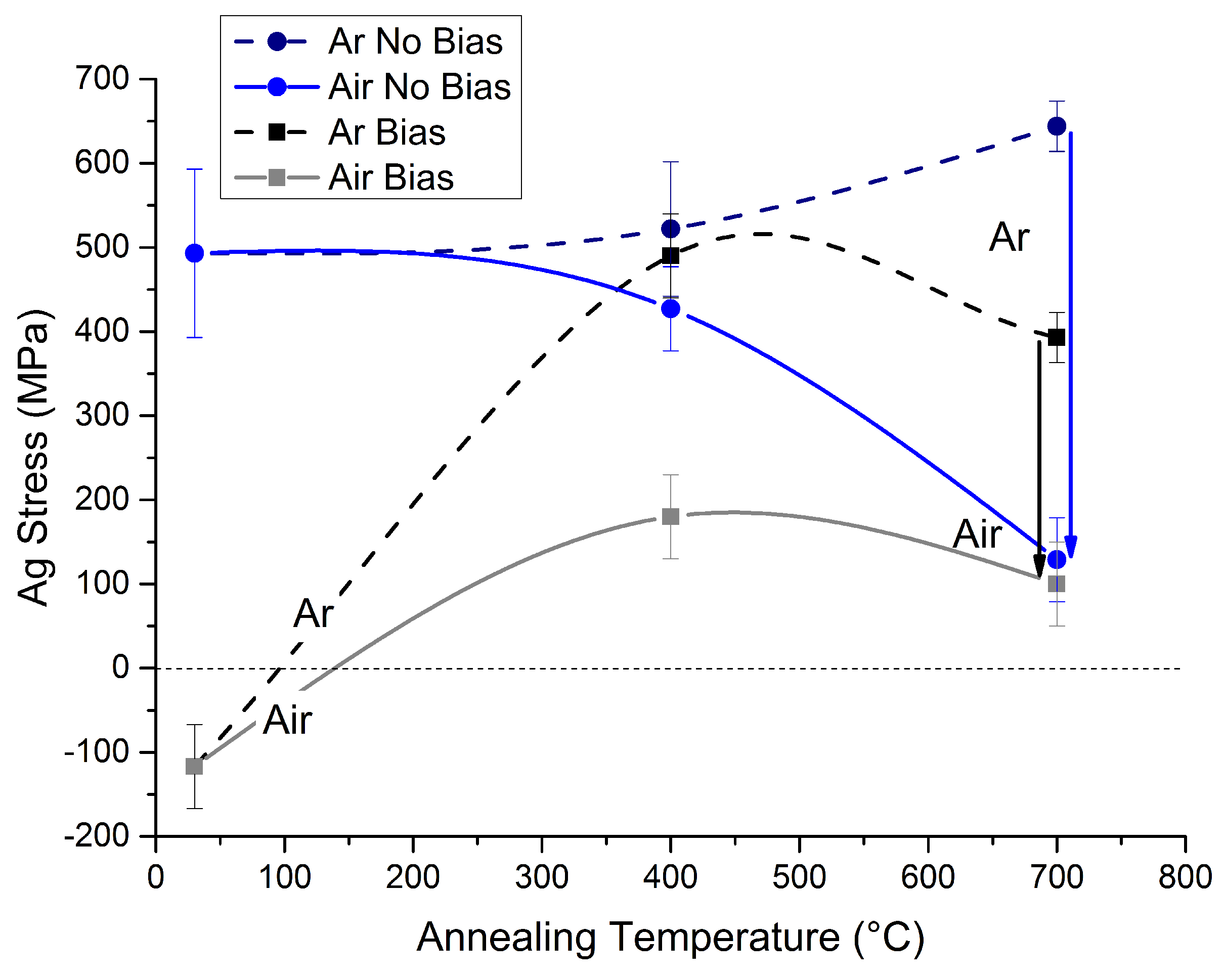
  • RF-bias application created disorder and roughness in the as deposited samples (both in planar and cross-sectional morphology) as well as a compressive state in Ag. The presence of Ge was found to smooth the Ag/AlN interface which appeared flatter and more regular in comparison with the Ag/AlN system.
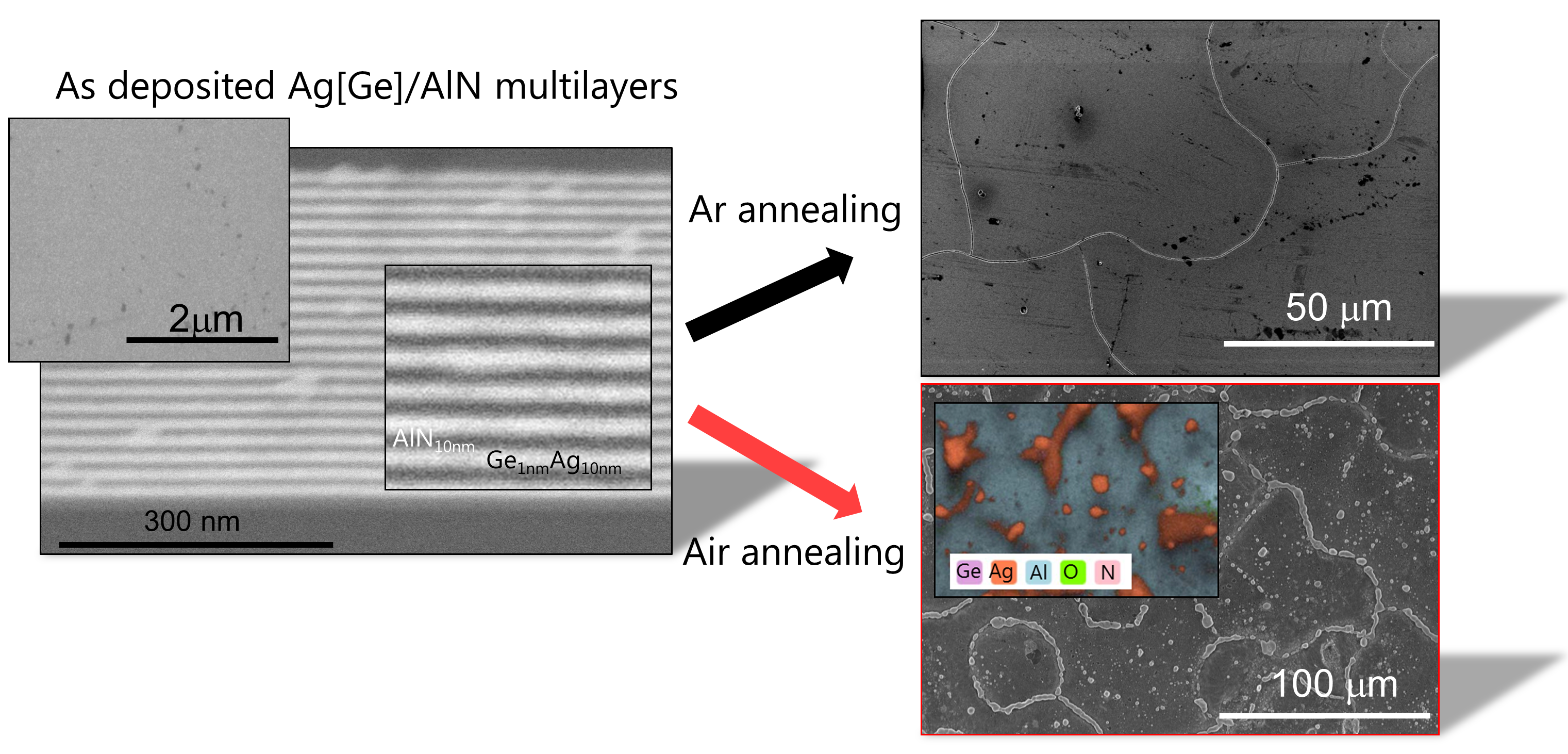
  • Wrinkling and cracking were observed at temperatures ≥400 C in air and Ar depending on the initial stress state of the system: compressive for bias samples leading to wrinkling and tensile for non-bias samples leading to cracking. The presence of Ge was determined to change the internal stress state in the Ag layers from compressive to tensile in non-bias samples in the as-deposited state.
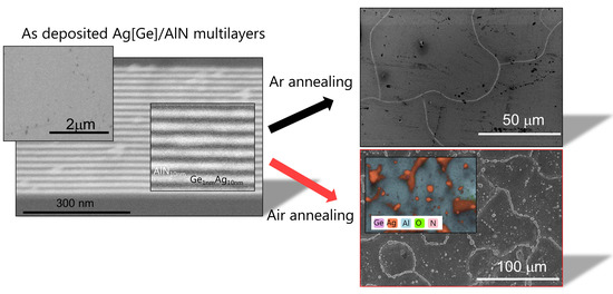
  • The Ag surface migration is observed prominently in air at 700 C for both, bias and non-bias samples, mostly through the previously formed cracks (at 400 C) due to stress relaxation. However, the Ag amount on the surface was found to be considerably lower in comparison with Ag/AlN systems annealed at 400 C.
  • The presence of Ge was proved to hinder the Ag mobility and diffusion at high temperatures in air. Ge accumulation was measured close to Ag particle on the surface.
  • Minimal Ag surface migration is observed for all the samples annealed in Ar at any temperatures. In particular, for non-bias samples, the high temperature treatment in Ar atmosphere is found to create a network of cracks extending all over the sample surface . These samples preserve the multilayer periodic ordered structure and keep a high internal tensile stress state up to 700 C.
The present study demonstrates the feasibility to reverse the stress state of as-deposited NML structures (from tensile to compressive) by changing the substrate bias and/or by interfacial modification and consequently affect the thermal evolution and stability. This paves the way for advanced experimental strategies to tailor directional mass outflow in nanoconfined filler systems for advanced nano-joining applications.

Author Contributions

Conceptualization, L.P.H.J., C.C., E.K. and J.J.-R.; Methodology, M.C.; Validation, J.J.-R., L.P.H.J. and C.C.; Formal Analysis, M.C.; Investigation, E.K.; Data Curation, C.C. and E.K.; Writing—Original Draft Preparation, C.C.; Writing—Review and Editing, C.C., E.K., L.P.H.J., J.J.-R.; Supervision, L.P.H.J.; Project Administration, J.J.-R.; Funding Acquisition, J.J.-R.

Funding

This research was funded by EXMONAN Grant No. EU FP7-PEOPLE-2013- IRSES Project EXMONAN.

Acknowledgments

The authors acknowledge Vicente Araullo-Peters and Michael Stiefel for the help in SEM characterization. The authors acknowledge the financial support of EU FP7-PEOPLE-2013-IRSES Project EXMONAN—Experimental investigation and modelling of nanoscale solid state reactions with high technological impact.

Conflicts of Interest

The authors declare no conflict of interest.

References

  1. Lloyd, S.J.; Molina-Aldareguia, J.M. Multilayered materials: A palette for the materials artist. Philos. Trans. R. Soc. Lond. A 2003, 361, 2931–2949. [Google Scholar] [CrossRef] [PubMed]
  2. Janczak-Rusch, J.; Kaptay, G.; Jeurgens, L.P.H. Interfacial Design for Joining Technologies: An Historical Perspective. J. Mater. Eng. Perform. 2014, 23, 1608–1613. [Google Scholar] [CrossRef]
  3. Fernando, G. Metallic Multilayers and Their Applications: Theory, Experiments, and Applications Related to Thin Metallic Multilayers; Elsevier: Amsterdam, The Netherlands, 2011; Volume 4. [Google Scholar]
  4. Stueber, M.; Holleck, H.; Leiste, H.; Seemann, K.; Ulrich, S.; Ziebert, C. Concepts for the Design of Advanced Nanoscale PVD Multilayer Protective Thin Films. J. Alloys Compd. 2009, 483, 321–333. [Google Scholar] [CrossRef]
  5. Cahn, J.; Larché, F. A simple model for coherent equilibrium. Acta Metall. 1984, 32, 1915–1923. [Google Scholar] [CrossRef]
  6. Moszner, F.; Cancellieri, C.; Chiodi, M.; Yoon, S.; Ariosa, D.; Janczak-Rusch, J.; Jeurgens, L. Thermal Stability of Cu/W Nano-multilayers. Acta Mater. 2016, 107, 345–353. [Google Scholar] [CrossRef]
  7. Tamleh, S.; Rezaei, G.; Jalilian, J. Stress and strain effects on the electronic structure and optical properties of ScN monolayer. Phys. Lett. A 2018, 382, 339–345. [Google Scholar] [CrossRef]
  8. Chiodi, M.; Cancellieri, C.; Moszner, F.; Andrzejczuk, M.; Janczak-Rusch, J.; Jeurgens, L.P. Massive Ag migration through Metal/Ceramic Nano-multilayers: An interplay between Temperature, Stress-Relaxation and Oxygen-Enhanced Mass Transport. J. Mater. Chem. C 2016, 4, 4927–4938. [Google Scholar] [CrossRef]
  9. Pigozzi, G.; Antušek, A.; Janczak-Rusch, J.; Parlinska-Wojtan, M.; Passerone, D.; Antonio Pignedoli, C.; Bissig, V.; Patscheider, J.; Jeurgens, L.P. Phase Constitution and Interface Structure of Nano-sized Ag-Cu/AlN Multilayers: Experiment and ab initio Modeling. Appl. Phys. Lett. 2012, 101, 181602. [Google Scholar] [CrossRef]
  10. Agarwal, S.; Herman, H. Liquid-quenched Ag-Ge Alloys; Formation and Evolution of Metastable phases. J. Mater. Sci. 1977, 12, 2021–2027. [Google Scholar] [CrossRef]
  11. Wang, Z.; Jeurgens, L.P.H.; Sigle, W.; Mittemeijer, E.J. Observation and Origin of Extraordinary Atomic Mobility at Metal-Semiconductor Interfaces at Low Temperatures. Phys. Rev. Lett. 2015, 115, 016102. [Google Scholar] [CrossRef] [PubMed]
  12. Flötotto, D.; Wang, Z.M.; Jeurgens, L.P.H.; Bischoff, E.; Mittemeijer, E.J. Effect of adatom surface diffusivity on microstructure and intrinsic stress evolutions during Ag film growth. J. Appl. Phys. 2012, 112, 043503. [Google Scholar] [CrossRef]
  13. Stefaniuk, T.; Olivier, N.; Belardini, A.; McPolin, C.; Sibilia, C.; Wronkowska, A.A.; Wronkowski, A.; Szoplik, T.; Zayats, A.V. Self-Assembled Silver–Germanium Nanolayer Metamaterial with the Enhanced Nonlinear Response. Adv. Opt. Mater. 2017, 5, 1700753. [Google Scholar] [CrossRef]
  14. Wróbel, P.; Stefaniuk, T.; Trzcinski, M.; Wronkowska, A.A.; Wronkowski, A.; Szoplik, T. Ge Wetting Layer Increases Ohmic Plasmon Losses in Ag Film due to Segregation. ACS Appl. Mater. Interfaces 2015, 7, 8999–9005. [Google Scholar] [CrossRef] [PubMed]
  15. Ariosa, D.; Cancellieri, C.; Araullo-Peters, V.; Chiodi, M.; Klyatskina, E.; Janczak-Rusch, J.; Jeurgens, L.P.H. Modeling of Interface and Internal Disorder Applied to XRD Analysis of Ag-Based Nano-Multilayers. ACS Appl. Mater. Interfaces 2018, 10, 20938–20949. [Google Scholar] [CrossRef] [PubMed]
  16. Furgeaud, C.; Simonot, L.; Michel, A.; Mastail, C.; Abadias, G. Impact of Ge alloying on the early growth stages, microstructure and stress evolution of sputter-deposited Cu-Ge thin films. Acta Mater. 2018, 159, 286–295. [Google Scholar] [CrossRef]
  17. Lee, J.W.; Tien, S.K.; Kuo, Y.C. The effects of substrate bias, substrate temperature, and pulse frequency on the microstructures of chromium nitride coatings deposited by pulsed direct current reactive magnetron sputtering. J. Electron. Mater. 2005, 34, 1484–1492. [Google Scholar] [CrossRef]
  18. Kovac, H.S.; Zoch, H. Influence of Substrate Bias Voltage on the Properties of Sputtered Aluminum-Scandium Thin Sheets. J. Surf. Eng. Mater. Adv. Technol. 2012, 2, 115–119. [Google Scholar] [CrossRef]
  19. Suzuki, M.; Maekawa, T.; Okano, S.; Bandow, T. Effects of rf-Bias on Properties of Sputtered Silicon Films. Jpn. J. Appl. Phys. 1981, 20, L485. [Google Scholar] [CrossRef]
  20. Wei, Y.; Gong, C. Effects of Pulsed Bias Duty Ratio on Microstructure and Mechanical Properties of TiN/TiAlN Multilayer Coatings. Appl. Surf. Sci. 2011, 257, 7881–7886. [Google Scholar] [CrossRef]
  21. Stryhalski, J.; Fontana, L.C.A.; Odorczyk, M.F.; Scholtz, J.S.; Sagas, J.C.A.; Recco, A.A. Pulsed bias effect on crystallinity and nano-roughness of Ti6Al4V-N films deposited by grid assisted magnetron sputtering system. Mater. Res. 2014, 17, 1545–1549. [Google Scholar] [CrossRef] [Green Version]
  22. Clemens, B.M.; Gay, J.G. Effect of layer-thickness fluctuations on superlattice diffraction. Phys. Rev. B 1987, 35, 9337–9340. [Google Scholar] [CrossRef]
  23. Coupeau, C. Atomic force microscopy study of the morphological shape of thin film buckling. Thin Solid Films 2002, 406, 190–194. [Google Scholar] [CrossRef]
  24. Logeeswaran, V.; Kobayashi, N.P.; Islam, M.S.; Wu, W.; Chaturvedi, P.; Fang, N.X.; Wang, S.Y.; Williams, R.S. Ultrasmooth Silver Thin Films Deposited with a Germanium Nucleation Layer. Nano Lett. 2009, 9, 178–182. [Google Scholar] [CrossRef] [PubMed]
  25. Chason, E.; Sheldon, B.W.; Freund, L.B.; Floro, J.A.; Hearne, S.J. Origin of Compressive Residual Stress in Polycrystalline Thin Films. Phys. Rev. Lett. 2002, 88, 156103. [Google Scholar] [CrossRef] [PubMed]
  26. Yim, W.M.; Paff, R.J. Thermal expansion of AlN, sapphire, and silicon. J. Appl. Phys. 1974, 45, 1456–1457. [Google Scholar] [CrossRef]
  27. Shenoy, V.; Schwartzman, A.; Freund, L. Crack patterns in brittle thin films. Int. J. Fract. 2001, 109, 29–45. [Google Scholar] [CrossRef]
  28. Teixeira, V. Residual stress and cracking in thin PVD coatings. Vacuum 2002, 64, 393–399. [Google Scholar] [CrossRef]
  29. Bracht, H.; Stolwijk, N.A. Diffusion in Si, Ge, and their alloys—Introduction. In Diffusion in Semiconductors; Beke, D.L., Ed.; Springer: Berlin/Heidelberg, Germany, 1998; pp. 1–11. [Google Scholar]
  30. Welzel, U.; Ligot, J.; Lamparter, P.; Vermeulen, A.C.; Mittemeijer, E.J. Stress analysis of polycrystalline thin films and surface regions by X-ray diffraction. J. Appl. Crystallogr. 2005, 38, 1–29. [Google Scholar] [CrossRef] [Green Version]
  31. Clemens, B.; Bain, J. Stress Determination in Textured Thin Films Using X-ray Diffraction. MRS Bull. 1992, 17, 46–51. [Google Scholar] [CrossRef]
Figure 1. (a) schematic representation of the Ag[Ge]/AlN NMLs studied and (b) the parameters changed during deposition and subsequent thermal annealing.
Applsci 08 02403 g001
Figure 2. SEM micrographs in planar (top) and cross-sectional (bottom) view of the Ag[Ge]/AlN NMLs produced (a) without substrate bias and (b) with substrate bias.
Applsci 08 02403 g002
Figure 3. Pole figures of Ag 111 and AlN 10 1 ¯ 3 family of planes, as recorded from for the as deposited NMLs, produced (a) without substrate bias and (b) with substrate bias. The same pole figures as acquired after annealing of the NMLs in Ar at 700 C are shown in (c,d).
Applsci 08 02403 g003
Figure 4. XRD scans of samples annealed at different temperatures for bias and non-bias samples, annealed in Ar (a,c) and in air (b,d), respectively. The arrows in (c) indicate the satellite appeareance pointing out a smoother interface upon annealing.
Applsci 08 02403 g004
Figure 5. SEM planar images of samples annealed at 400 C in air (a) without bias and (b) with bias; (c) cross section SEM of (a) through a crack with Ag outflow; (d) SEM cross section of (b) through a wrinkle. The inset in (b) is the elemental EDX analysis.
Applsci 08 02403 g005
Figure 6. SEM micrographs in planar (top) and cross-sectional view (bottom) of the Ag[Ge]/AlN NMLs, as deposited without bias, after annealing at 700 C (a) in Ar and (c) in air. Corresponding SEM micrographs of the Ag[Ge]/AlN NMLs, as deposited witht bias, after annealing at 700 C (b) in Ar and (d) in air; (e) EDX mapping of (d) which shows that the surface particles are pure Ag and close to them there are Germanium-enrinched surface regions (indicated by arrows).
Applsci 08 02403 g006
Figure 7. Ag in-plane stress results for the different annealing temperatures and atmospheres, measured ex-situ, at room temperature, for samples with and without bias.
Applsci 08 02403 g007

