Article

Accurate Models for Evaluating the Direct Conducted and Radiated Emissions from Integrated Circuits

by
Domenico Capriglione
1,
Andrea G. Chiariello
2 and
Antonio Maffucci
3,*
1
Department of Industrial Engineering, University of Salerno, Campus di Fisciano, 84084 Fisciano, Italy
2
Department of Engineering, University della Campania L. Vanvitelli, Via Roma 29, 81031 Aversa, Italy
3
Department of Electrical and Information Engineering, University of Cassino and Southern Lazio, via G. Di Biasio 43, 03043 Cassino, Italy
*
Author to whom correspondence should be addressed.
Appl. Sci. 2018, 8(4), 477; https://doi.org/10.3390/app8040477
Submission received: 17 January 2018 / Revised: 1 March 2018 / Accepted: 20 March 2018 / Published: 21 March 2018

Abstract

:

Featured Application

Inclusion of the electromagnetic compatibility analysis in the design phase of the production flux of high-speed integrated circuits.

Abstract

This paper deals with the electromagnetic compatibility (EMC) issues related to the direct and radiated emissions from a high-speed integrated circuits (ICs). These emissions are evaluated here by means of circuital and electromagnetic models. As for the conducted emission, an equivalent circuit model is derived to describe the IC and the effect of its loads (package, printed circuit board, decaps, etc.), based on the Integrated Circuit Emission Model template (ICEM). As for the radiated emission, an electromagnetic model is proposed, based on the superposition of the fields generated in the far field region by the loop currents flowing into the IC and the package pins. A custom experimental setup is designed for validating the models. Specifically, for the radiated emission measurement, a custom test board is designed and realized, able to highlight the contribution of the direct emission from the IC, usually hidden by the indirect emission coming from the printed circuit board. Measurements of the package currents and of the far-field emitted fields are carried out, providing a satisfactory agreement with the model predictions.

1. Introduction

The current technology trends push towards the realization of integrated circuits (ICs) characterized by smaller size, lower power supply voltages, and higher operating frequencies [1]. In addition, conventional solutions are no longer applicable and, therefore, a great amount of effort is given to finding new materials (such as the use of nanomaterials [2]) and/or new architectures (e.g., the 3D integration [3]).
These design trends are followed to strongly enhance IC performance, but give rise to serious electromagnetic compatibility (EMC) issues, such us unwanted conducted and radiated emissions and, in general, undesired electromagnetic interference (EMI) problems [4,5,6]. The reduction and mitigation of IC emissions have recently become of great interest in application fields, like automotive or consumer electronics, since it allows to fulfill the EMC requirements without the burden of the classical solutions to such problems, such as the use of filters or shields.
Therefore, nowadays an IC-level characterization of EMC issues is needed, whereas, in the past, these issues have been typically studied at the printed circuit board (PCB) level [7]. The IC-conducted emission is mainly due to the switching activity, hence, an accurate modeling must be implemented to evaluate the switching pulsed current flowing from the IC to the PCB [8]. The conducted emission is also dangerous because it can easily convert into radiated emission when such currents flow across PCB traces and cables that can act as emitting antennae. As for the radiated emission, the contribution of the radiation coming from the package lead frame or circuits routed at the silicon level (“direct radiation”) is no longer negligible with respect to the radiation coming from the PCB (“system level radiation”) and must be taken under control, to avoid any interference with nearby circuitry. Therefore, both direct IC radiation [9,10] and system-level radiation [11,12] have been studied by means of measurements and numerical simulations.
The requirements and limits imposed by the EMC norms are set for the final product and not for the single subpart, therefore, traditionally EMC testing (including EMI analysis) was usually performed at a very late stage of product development, namely, on the complete prototype. As a consequence, only at that stage was it possible to choose the solutions needed to mitigate these problems. Given today’s operating frequencies, such an approach can be very costly and time consuming and, hence, the EMC/EMI issues must be included at the design level. This can be done, in principle, by means of a full-chip simulation, which, however, results in being extremely cumbersome. Therefore, several alternative approaches have been proposed, typically based on a segmentation technique, where any single subpart of the system is described with a proper equivalent circuit model.
This paper proposes two models: a circuital model to simulate the currents flowing from the IC to the package pins, where the IC and the package is modeled by a lumped circuit and the board by a distributed one. An electromagnetic model is then derived to estimate the far-field direct emission from the IC, using the outputs of the circuital model (i.e., the package currents), regarded as the sources of the field problem.
The paper is organized as it follows. Section 2 illustrates the circuital and the electromagnetic models and discusses the design and setups of the experiments. In Section 3, the identification of the model parameters is carried out and the experimental validation of the models is presented. A detailed discussion of the simulation and the measurement results is also provided.

2. Materials and Methods

2.1. Circuital Model for Evaluating the Conducted Emission

In order to provide to the designers simple and effective tools for simulating the impact of an IC on the EMC performance of a complex system made by an IC, package, and PCB, suitable equivalent circuital models have been proposed over the years. A first attempt to provide an IC circuit model was the so-called IBIS model, based on the “Input/output buffer information specifications”, hence, on the characterization of the electrical performance at the terminal pins of an IC [13]. This model has the advantage of simplicity, but shows major drawbacks coming from the lack of inclusion of main phenomena, such as the switching noise and the load effect of the PCB. An enhanced circuital model for the IC conducted emission has been proposed, for instance, in [14], based on the so-called “linear equivalent circuit and current source” model.
More recently, the International Electrotechnical Commission proposed the so-called Integrated Circuit Emission Model (ICEM), with the purpose to accurately take into account the internal activity of the ICs [15,16]. The ICEM model has been successfully used over the years to carry out performance analysis of ICs, in terms of emission, immunity, jitter, and so on [9,17,18]. The limitation of this model in terms of maximum operating frequencies can be easily removed, as recently shown in [8], by taking into account the effects of the loads (specifically the transmission lines of the PCB) with a distributed model. This paper adopts the latter approach to derive a circuit model in the frame of the ICEM standard. Specifically, the high-frequency behavior of the PCB is described by exploiting its S-parameter characterization.
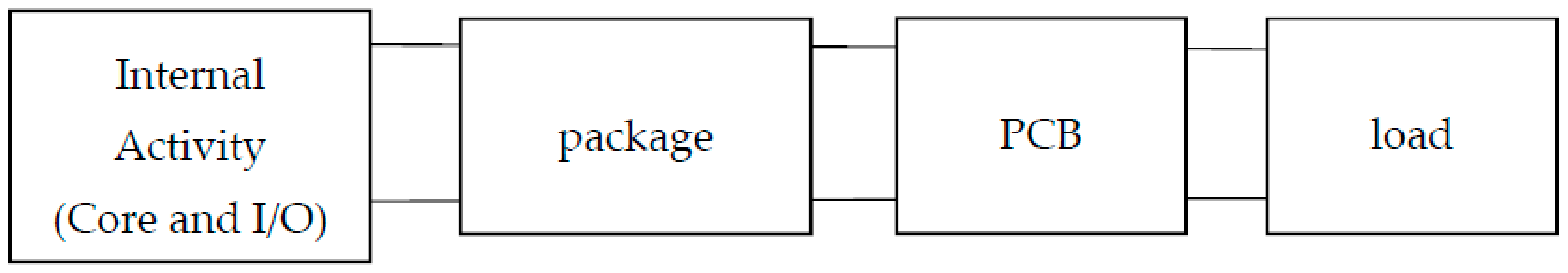
The conceptual scheme of the adopted approach is reported in Figure 1, showing the overall circuit as composed of four main subparts: the first subpart (internal activity, IA) describes the core and the I/O buffers, the second one describes the package, whereas the third one refers to the printed circuit board (PCB). The final subpart represents a generic load that simulates a buffer that exchanges data with the IC. The above subdivision is based on the features of the circuit models to be adopted for the different subparts: for the IA the circuit is active and lumped, for the IC it is passive and lumped, whereas for the PCB it is passive and distributed.
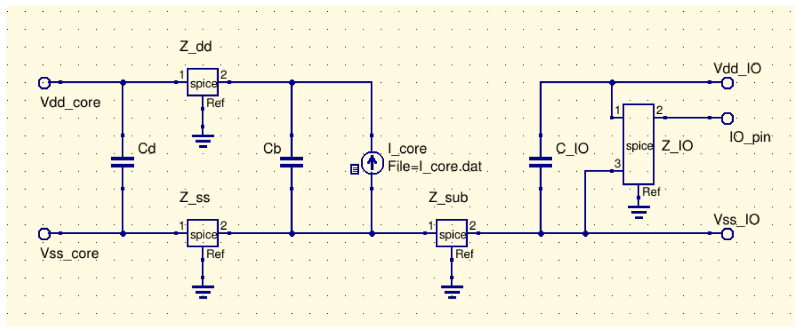
According to the ICEM model [16], the first subpart is modelled as in Figure 2, where the core activity is represented by an equivalent current source Icore, and the parasitic of the supply rails are given by series impedance R-L, Zdd and Zss, which also separates the decoupling into two contributions: Cd, between Vdd and Vss, and Cb, close to the current generator Icore. The core model is coupled to the I/O buffer, which is described here by means of an IBIS model [13]. In the IC analyzed in this paper, the core supply and the I/O supply are separated and, thus, according to the ICEM rules [16] the coupling model must contain a substrate impedance Zsub, and an additional decoupling capacitor CI/O. The Vdd and Vss pins at the left and right side of 
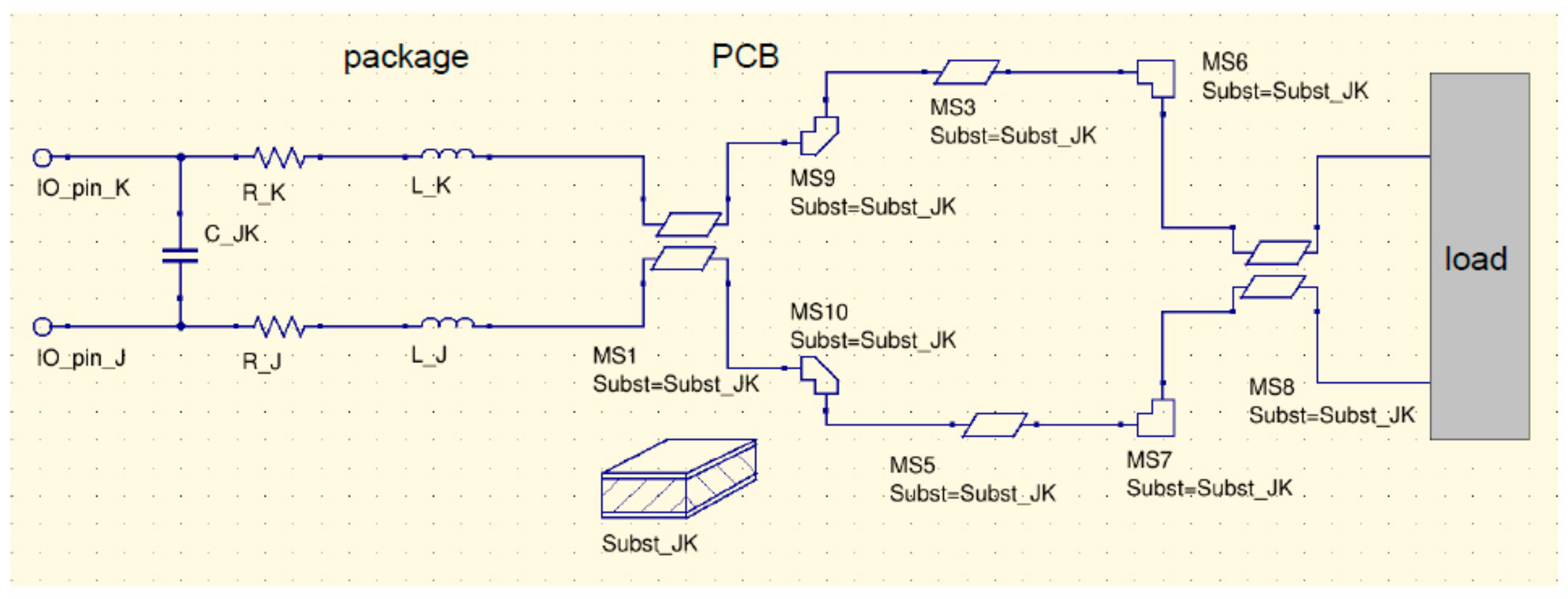
Figure 2 are connected to the corresponding pins of the package. Each I/O pin is connected to the corresponding signal interconnect at the package and the PCB level, as shown in the circuit model in Figure 3, which also reports the parasitics for the package interconnects and the equivalent circuital models for the PCB traces.
In this paper, as specified in Section 3, the IA circuit model has been obtained from a transistor-level simulation. Alternatively, a characterization based on measurements can be carried out, following the standards set in [19]. The advantage of this approach is that no internal description of the IC is required, but the main disadvantages are the need to de-embed the text-fixture and the impossibility to directly measure the current Icore. Such a current must be derived from indirect measurement of currents flowing in the board traces, by using, for instance, identification techniques like the backward current division rule, as shown in [20]. An alternative model for the current sources is based on a harmonic decomposition, as proposed in [8].
The subpart “package” takes into account all passive elements in the package. As described in Figure 3, all these passives are modeled with lumped elements (RLC) and are extracted here by a quasi-static field solver. Indeed, this assumption is valid if the components are electrically short, namely:
l c λ m i n = v f m a x
where l c is the characteristic length of the component, v is the propagation velocity and f m a x is the maximum frequency of the signals. Condition (1) is always verified for IC passives up to frequencies of the order of tens of GHz (mm-wavelength), since the maximum lenghts of nowadays on-chip interconnects are of the order of hundreds of microns (e.g., typical values of a global level interconnect length for 22 and 14 nm technology nodes [1]).
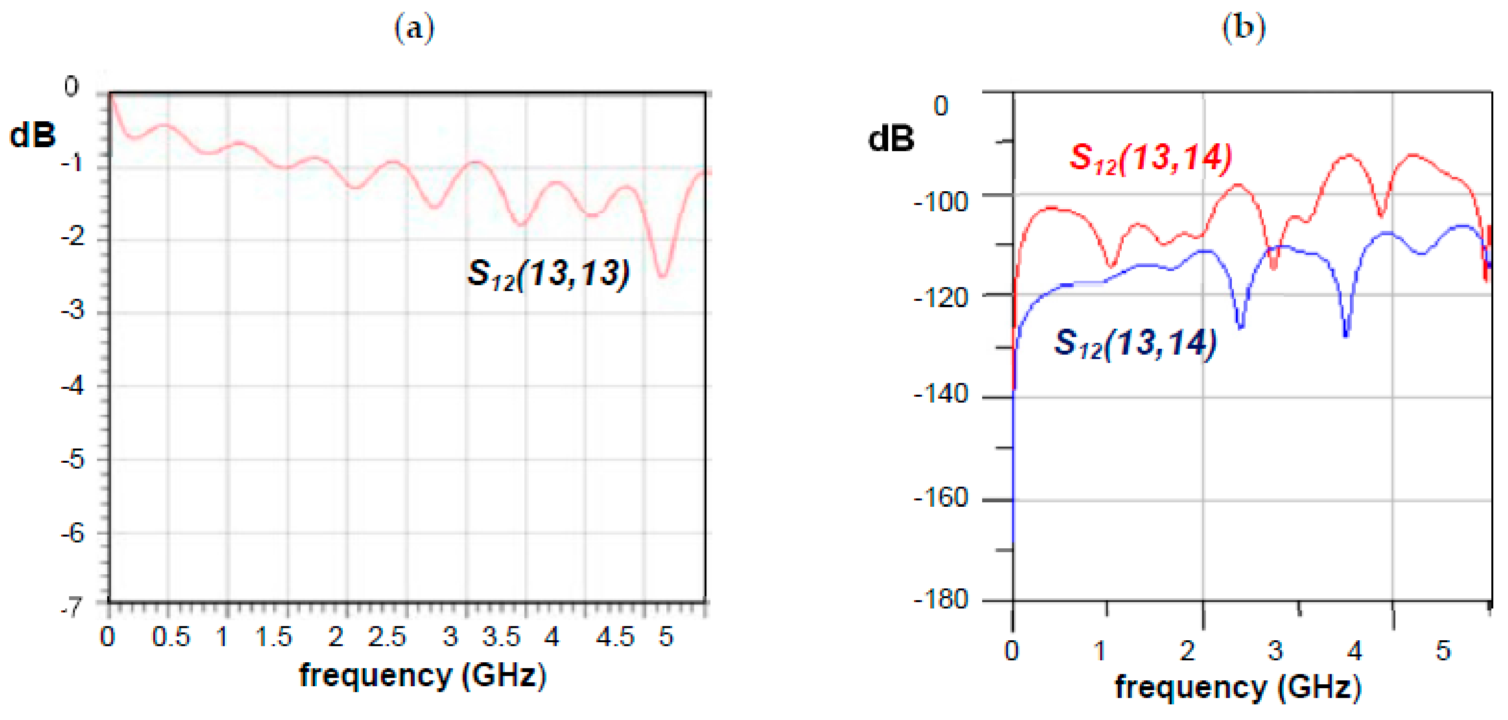
Finally, the subpart “PCB” is modeled through a distributed circuit, namely an equivalent transmission line (TL). Indeed, as pointed out in [8], the use of a distributed model for the PCB allows extending to higher frequencies (tens of GHz) the validity limit of the classical ICEM models. Specifically, this distributed subpart is here modelled in the overall circuit by means of a low-order equivalent macromodel synthezised from the PCB multiport admittance matrix, Y. In turn, according to the TL theory [21], such a matrix can be obtained from the scattering matrix, S, as:
Y = ( S + I ) 1 ( S I ) Z 0 1
where Z 0 is a reference impedance value (usually taken as 50 Ω) and I is the identity matrix. Indeed, the S-parameters are the natural frame for a high-frequency characterization of a PCB, either based on full-wave simulations (as done in this paper) or on measurements. After the Y-matrix is retrieved from Equation (2), a low-order equivalent circuit may be derived through a synthesis procedure based on the vector fitting technique, as in [22]. Indeed, the generic entry of the admittance matrix can be expressed in terms of a truncated series of pole-residue pairs:
Y i j ( s ) = m = 1 N R i j , m s p i j , m + R i j , 0 ,
and the pole-residue pairs may be associated to R-L or R-C branches in the final circuit model [22].

2.2. Electromagnetic Model for Evaluating the Radiated Emission

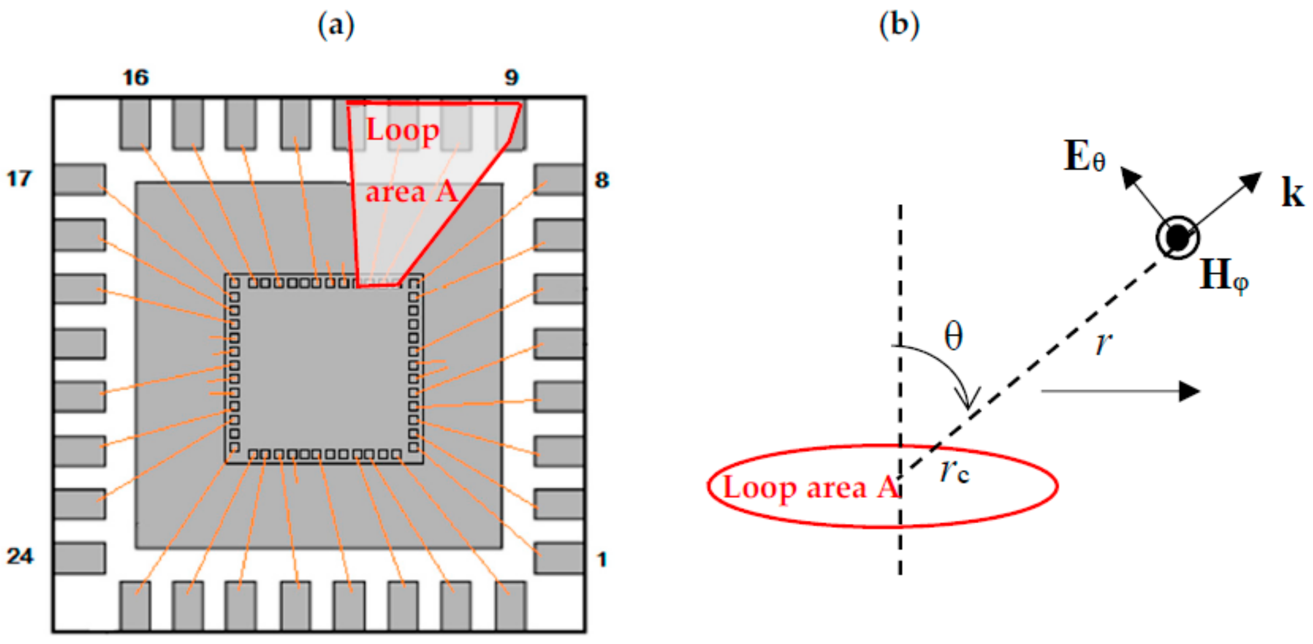
A main goal of this paper is the evaluation of the direct radiated emission from an IC in the far-field zone, assuming to know the currents flowing from the IC into the package. These currents are indeed the output of the circuit model developed in Section 2.1, hence, the electromagnetic problem is cast in terms of the emission of known currents in the far-field zone. This field may be computed at a distance r by superimposing the contribution of each current loop in the package (see Figure 4a), if the following conditions hold [23]:
r c < λ m i n 6 π ,   r r c ,
being r c the average value of the loop radius. For typical package dimensions of today’s ICs (of the order of mm × mm), Equation (4) is fulfilled for frequencies up to the order of GHz. In the same assumption, a very good approximation of a small loop is the infinitesimal loop (or the infinitesimal magnetic dipole), whose far fields (see Figure 4b) are given in the frequency domain by [23]:
E θ ( r , f ) = I ( f ) η β 2 A e j β r 4 π r sin θ ,   H φ ( r , f ) = E θ ( r , f ) η
where I(f) is the spectrum of the loop current, η = 377   Ω is the intrinsic impedance, β is the wavenumber, and A is the loop area. Note that the presence of a grounded metallic layer at the opposite side of the board where the package will be mounted can be taken into account by applying the image theorem, thus, by taking into account the contribution coming from image currents located by symmetry at opposite sides of the ground plane. In principle, vertical tracts of the package-to-board interconnects should be also taken into account if the area of the corresponding loop currents is comparable to that of the horizontal loops in Figure 4a. However, this is not the case for the application studied in this paper, where the vertical tracts of the interconnects to the pins are much smaller in length with respect to the horizontal ones.

2.3. Experiment Design and Setup

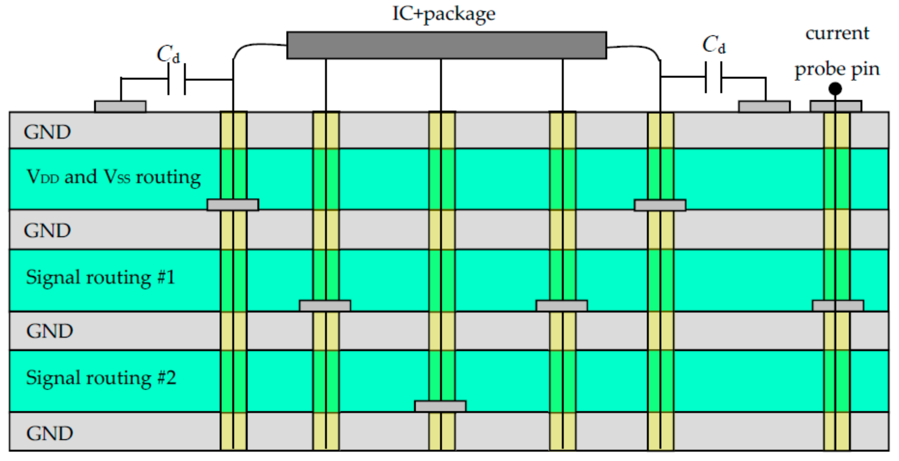
In this paper, an IC from the 110 nm technology node has been studied, mounted on a quad-flat package. A custom test board has been specifically designed to minimize the effect of the PCB on the conducted and radiated emission, see Figure 5. A multilayered structure has been adopted, where the package pins are directly connected to vertical vias, and then routed in inner layers. In this way, no trace is routed on the upper side of the board, so avoiding indirect radiation. The power traces (Vdd and Vss) are routed in different layers with respect to the signal traces, to avoid any effect of coupling between power and signal subsections. In addition, the signal traces connected to adjacent package pins are routed in different layers, in order to mitigate the high-frequency crosstalk effect. Specifically, in the board used for the conducted emission test, additional traces are routed independently to the board surface to provide contact points for the current probes. In the board used for radiated emission, addition bottom layers are included, where no signal is routed and no via is connected. The presence of blind vias and of electromagnetically-decoupled bottom layers minimize the contribution to the emitted field possibly related to parasitic cavity resonances.
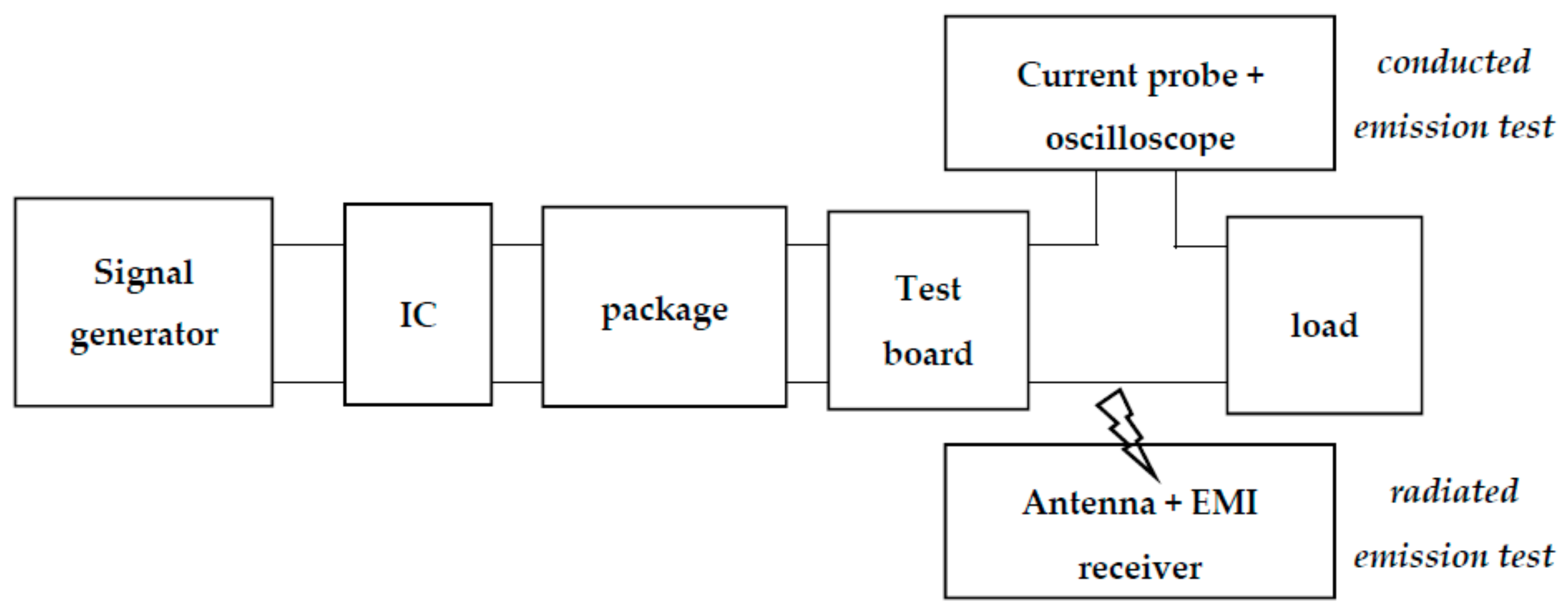
The block diagrams of the experimental setups used for evaluating the conducted and radiated emissions is schematically reported in Figure 6. For both cases, the test board is terminated on a load simulating a buffer that exchanges data with the IC, so that the emission analysis is performed while the equipment is operating in nominal conditions, as requested by the EMC norms [24,25,
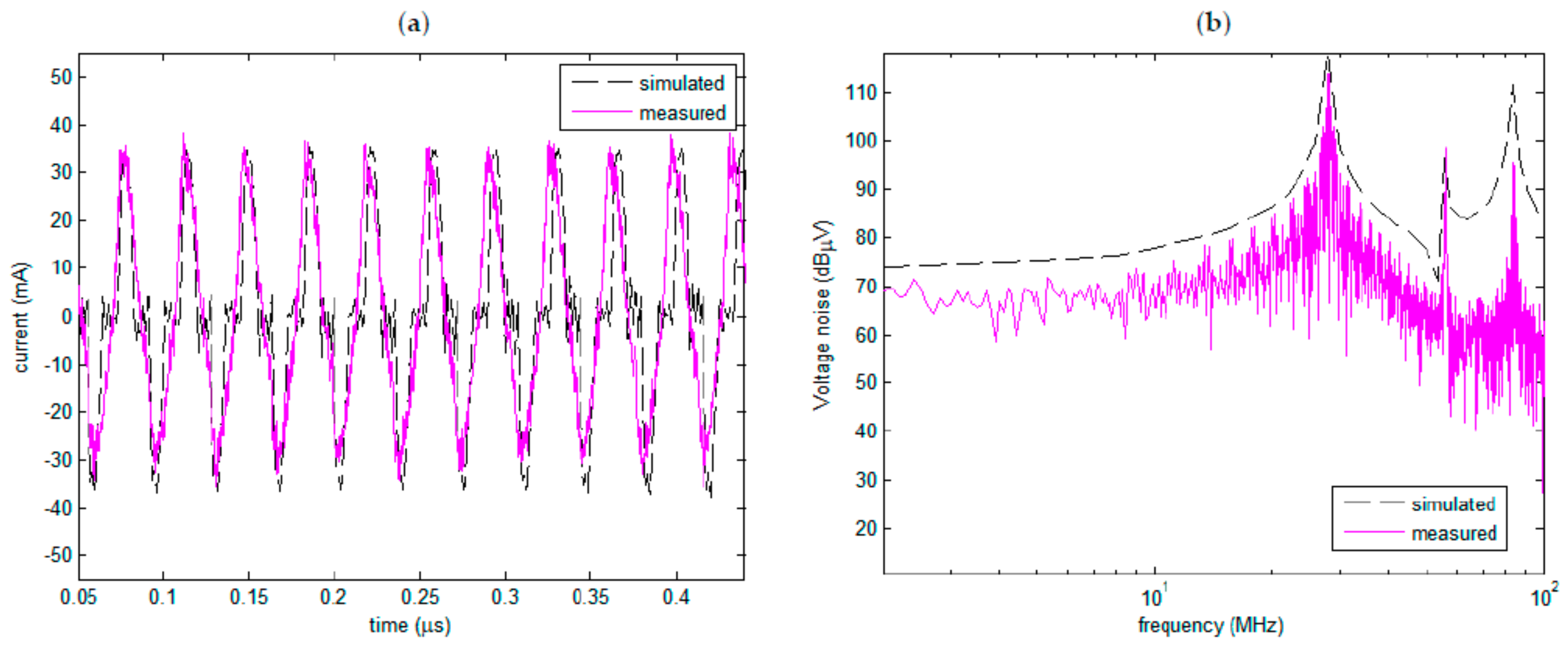
26]. To this end, a signal generator (Keysight, US: model N9310A, bandwidth 9 kHz–3 GHz) was connected, with an internal impedance of 50 Ω in the considered range, in parallel to a 40 pF capacitor representing a buffer. As for the conducted emission test, the currents have been acquired at the test board pads by a current probe (Lecroy D410-A-PS, bandwidth 4 GHz), then sent to an oscilloscope (LeCroy, Korea: model WavePro 7 Zi-A oscilloscope, bandwidth 6 GHz, 40 GS/s). The adopted measurement chain accounts for a maximum measurement uncertainty of ±2.5 dB on the considered frequency range.
With reference to the radiated emission test, the far-field electrical field has been collected by a broadband receiving antenna (a biconical-log antenna HL, Czech, model HL-1000, bandwidth 30 MHz–1 GHz) connected to an EMI receiver (R and S ESPC, bandwidth 9 kHz–2.5 GHz). Additionally, in this case, the maximum measurement uncertainty in the considered frequency range is ±2.5 dB. Specifically, a 3 m-radiated test was performed in a semi-anechoic chamber, according to the CISPR 16-4 standards for the radiated emission, in the frequency range from 30 MHz to 1 GHz [25]. A preliminary measurement with the device off has been performed to estimate the background noise and remove it from the results. The device under test was made by the IC mounted in its test board, connected to a signal generator through shielded cables, to avoid unwanted emission from interconnects.

3. Results

3.1. Identification of the Circuit Model

The IC studied in this paper belongs to the 110 nm technology node and is characterized by the parameters reported in Table 1. The emissions of the IC have been studied during a standard bit sequence defined by the IC supplier, representing a digital data transfer through the I/O pins. Specifically, three different conditions have been studied, referring to different choices of the data sequence frequency and rise time, and of the average nominal level (rms) of the currents injected into the pins (Table 2). In this paper, the overall circuit model has been implemented with the circuital simulation tool Qucs [27], see Figure 2 and Figure 3. The time-domain waveforms for Icore, and the values of the components in Figure 2 have been provided by the IC supplier, as the outputs of a transistor-level simulation of the IA, whereas the submodel describing the I/O buffer in Figure 2 have been imported by the IBIS library [13]. A quad-flat package has been used, with a total area of about 20 × 20 mm. The package parasitic lumped elements have been extracted by a quasi-static field simulator (Comsol Multiphysics [28]). The values of the electrical parameters of the package and of the decaps are summarized in Table 3.
The test board has been realized with a three layer PCB (see Figure 5), with the geometrical and electrical parameters provided in Table 4 (an FR-4 dielectric has been used). The PCB traces are designed to provide controlled impedances of 50 Ω ± 10% (in the frequency range 1 MHz–1 GHz) and equalized delays, in order to avoid signal integrity issues related to delay mismatching.
The PCB S-matrix has been computed by means of the FEM solver integrated into the full-wave commercial simulator CST Microwave Studio [29]. In the following, S11(n,n) and S12(n,n) represent the reflected and transmitted waves associated to the generic line n, whereas S11(n,m) and S12(n,m) represent the coupling coefficients between lines n and m at ports 1 and 2 and, hence, they may be taken as a measure of the near-end and the far-end crosstalk noise, respectively. Figure 7a shows, as an example, the computed parameter S12(13,13) (transmission along the trace #13), whereas Figure 7b shows the transmission from line #13 to two adjacent ones, S12(13,14) and S12(13,15). The behaviors shown in Figure 7 are representative of the results for all PCB traces and, thus, from Figure 7a, it is evident that the board traces are well matched to the reference impedance at least up to 1 GHz, since the transmission is almost perfect (at 1 GHz, S12 is still above −1 dB). From Figure 7b it results that the crosstalk noise is completely negligible, thanks to already-mentioned design guidelines adopted for the multilayered structure. After computing the S-parameters, the admittance matrix has been derived from (2) and then synthesized with a low-order approximation as in (3). The matrix entries in (3) have been implemented through the equivalent circuits in Figure 3. As an example, Table 5 shows the extracted values for the equivalent circuit elements for lines #38–40.

3.2. Conducted and Radiated Emission: Results and Discussion

The conducted emission has been measured by using the setup in Figure 6. The measurements have been compared with the simulations in Figure 8, which shows the results for Case 1 defined in Table 2. Specifically, Figure 8a shows the time-domain waveforms of simulated vs. measured currents at one of the pin pairs (data-ground), showing a satisfactorily agreement. Note that the numerical results are affected by ripples corresponding to the transitions across the zero level, which are not present in the measured results, due to low-pass filtering action of the instruments. These oscillations are due to the high-frequency effect of the L-C components in the IC equivalent circuits model, but do not affect the main features of the numerical results (e.g., rms value, frequency, etc.). Indeed, Table 6 provides the rms values of the currents injected into the package pins in the three different conditions of Table 2. The cases with higher frequency (cases 2 and 3) are associated to a higher level of the injected current.
The spectrum of the conducted emission noise in terms of voltage across a 50 Ω impedance is also reported in Figure 8b, using both simulated and measured results. The agreement is satisfactory in terms of peak values and position. Note that these voltage values cannot be compared to the EMC norm limits [24], since such a norm imposes the use of the so-called “1 Ω/150 Ω direct coupling method”. A comparison with the norm limits is, however, out of the scope of this paper.
Figure 9 shows the measured and simulated values of the far-field electric field evaluated at 3 m distance, assuming that the IC injects in the package pins the currents shown in Figure 8. Both the simulated and the measured values refer to the worst case condition, with respect to different polarization and incidence angles. Although the agreement is not as good as for the conducted emission, the results are quite satisfactory, since many of the emission peaks are correctly reproduced. Furthermore, the average level of the emission in the range 30 MHz–1 GHz is satisfactorily taken, as shown in Table 7, referring to the three different operating conditions of the IC defined in Table 2. The lower emission can be found in correspondence to Case 1, which refers to the lower frequency, the higher the rise time (see Table 2) and the lower value of the currents (Table 6). The worst condition is given by Case 3, corresponding to the higher frequency, the lower rise time (see Table 2) and the higher value of the currents (Table 6). As a conclusion, the direct emission is characterized by peak levels that can easily overcome the limits imposed by common EMC international norms for radiated emissions [25,26].

4. Conclusions

In this paper, a circuit and an electromagnetic model for evaluating, respectively, the conducted and the direct radiated emission from an integrated circuit has been developed and validated. An ICEM-based circuit model for the IC is augmented with proper lumped and distributed models for the passives (package and board). A loop-antenna model based on the superposition of the fields generated by given currents is used to evaluate the direct radiation. A suitable custom test-board has been designed and realized to evidence the effect of direct radiation, usually hidden by those indirectly coming from PCB traces. Despite its simplicity and modularity, the circuit model is shown to be able to accurately predict the time-domain waveforms of the currents injected by the IC into the package pins during its switching activity. As for the radiated emission, the model is able to catch its global level and many of the emission peaks. It has been shown that the direct emission from an IC cannot be neglected since it can attain levels comparable with the system level emission due to the board traces and other interconnects.

Acknowledgments

The work and the publishing costs have been partially funded by the EU H2020 EMPIR project “MICEV”, Metrology for Inductive charging of electric vehicles under grant # 16ENG08.

Author Contributions

The authors contributed equally to this work.

Conflicts of Interest

The authors declare no conflict of interest.

References

  1. International Technology Roadmap for Semiconductors, ITRS. Available online: www.itrs2.net (accessed on 8 January 2018).
  2. Maffucci, A. Carbon nanotubes in nanopackaging applications. IEEE Nanotechnol. Mag. 2009, 3, 22–25. [Google Scholar] [CrossRef]
  3. Radamson, H.H.; Zhang, Y.; He, X.; Cui, H.; Li, J.; Xiang, J.; Liu, J.; Gu, S.; Wang, G. The Challenges of Advanced CMOS Process from 2D to 3D. Appl. Sci. 2017, 7, 1047. [Google Scholar] [CrossRef]
  4. Ben Dhia, S.; Ramdani, M.; Sicard, E. Electromagnetic Compatibility of Integrated Circuits: Techniques for Low Emission and Susceptibility; Springer: New York, NY, USA, 2005. [Google Scholar]
  5. Ott, H. Electromagnetic Compatibility Engineering; Wiley: New York, NY, USA, 2011. [Google Scholar]
  6. Ramdani, M.; Sicard, E.; Boyer, A.; Ben Dhia, S.; Whalen, J.J.; Hubing, T.H.; Coenen, M.; Wada, O. The Electromagnetic Compatibility of Integrated Circuits—Past, Present, and Future. IEEE Trans. Electromagn. Compat. 2009, 51, 78–100. [Google Scholar] [CrossRef] [Green Version]
  7. Montrose, M.I. EMC and the Printed Circuit Board: Design, Theory, and Layout Made Simple; Wiley-IEEE Press: Hoboken, NJ, USA, 1998. [Google Scholar]
  8. Berbel, N.; Fernandez-Garcia, R.; Gil, I. Characterization and Modeling of the Conducted Emission of Integrated Circuits Up to 3 GHz. IEEE Trans. Electromagn. Compat. 2014, 56, 878–884. [Google Scholar] [CrossRef]
  9. Labussière-Dorgan, C.; Bendhia, S.; Sicard, E.; Tao, J.; Quaresma, H.J.; Lochot, C.; Vrignon, B. Modeling the Electromagnetic Emission of a Microcontroller Using a Single Model. IEEE Trans. Electromagn. Compat. 2008, 50, 22–34. [Google Scholar] [CrossRef]
  10. Fogle, A.D.; Darling, D.; Blish, R.C.; Daszko, G. Flash Memory Electromagnetic Compatibility. IEEE Trans. Device Mater. Reliab. 2006, 6, 266–276. [Google Scholar] [CrossRef]
  11. Park, H.H.; Jang, H.-T.; Park, H.-B.; Choi, C. An EMI Evaluation Method for Integrated Circuits in Mobile Devices. IEEE Trans. Electromagn. Compat. 2013, 55, 780–787. [Google Scholar] [CrossRef]
  12. Steinecke, T.; Goekcen, M.; Hesidenz, D.; Gstoettner, A. High-Accuracy Emission Simulation Models for VLSI Chips including Package and Printed Circuit Board. In Proceedings of the 2007 IEEE International Symposium on Electromagnetic Compatibility, Honolulu, HI, USA, 9–13 July 2007; pp. 1–6. [Google Scholar]
  13. International Electrotechnical Commission. IEC 62014-1: Electronic Design Automation Libraries—Part 1: Input/output Buffer Information Specifications (IBIS Version 3.2); IEC: Geneva, Switzerland, 2001. [Google Scholar]
  14. Ichikawa, K.; Inagaki, M.; Sakurai, Y.; Iwase, I.; Nagata, M.; Wada, O. Simulation of integrated circuit immunity with LECCS model. In Proceedings of the 2006 17th International Zurich Symposium on Electromagnetic Compatibility, Singapore, 27 February–3 March 2006; pp. 308–311. [Google Scholar]
  15. Lochot, C.; Levant, J.L. ICEM: A new standard for EMC of IC definition and examples. In Proceedings of the 2003 IEEE Symposium on Electromagnetic Compatibility, Boston, MA, USA, 18–22 August 2003; pp. 892–897. [Google Scholar]
  16. International Electrotechnical Commission (IEC). IEC 62014-3, Integrated Circuits Emission Model (ICEM); IEC: Geneva, Switzerland, 2004. [Google Scholar]
  17. Levant, J.L.; Mohamed, R.; Richard, P.; M’Hamed, D. EMC assessment at chip and PCB level: Use of the ICEM model for jitter analysis in an integrated PLL. IEEE Trans. Electromagn. Compat. 2007, 49, 182–191. [Google Scholar] [CrossRef]
  18. Yan, W.; Xu, X.; Kang, Q.; Wang, L. Modeling and Test Analysis of Electromagnetic Compatibility of a Power IC. Sens. Lett. 2014, 12, 207–212. [Google Scholar] [CrossRef]
  19. International Electrotechnical Commission (IEC). IEC 62433-2. Models of Integrated Circuits for EMI Behavioral Simulation—Conducted Emission Modelling (ICEM-CE); IEC: Geneva, Switzerland, 2006. [Google Scholar]
  20. Stievano, I.S.; Rigazio, L.; Maio, I.; Canavero, F.G. Behavioral Modeling of IC Core Power-Delivery Networks From Measured Data. IEEE Trans. Compon. Packag. Manuf. Technol. 2011, 1, 367–373. [Google Scholar] [CrossRef]
  21. Miano, G.; Maffucci, A. Transmission Lines and Lumped Circuits; Academic Press: Cambridge, MA, USA, 2001. [Google Scholar]
  22. De Magistris, M.; De Tommasi, L.; Maffucci, A.; Miano, G. Low-Order Identification of Interconnects with the Generalized Method of Characteristics. IEEE Trans. Electromagn. Compat. 2007, 49, 670–676. [Google Scholar] [CrossRef]
  23. Harrington, R.F. Time-Harmonic Electromagnetic Fields; IEEE Press: Hoboken, NJ, USA, 2001. [Google Scholar]
  24. International Electrotechnical Commission (IEC). IEC 61967-4, Integrated Circuits—Measurement of Electromagnetic Emissions, 150 kHz to 1 GHz—Part 4: Measurement of Conducted Emissions, 1 ohm/150 ohm Direct Coupling Method; IEC: Geneva, Switzerland, 2002. [Google Scholar]
  25. International Electrotechnical Commission (IEC). CISPR 32: Electromagnetic Compatibility of Multimedia Equipment—Emission Requirements; IEC: Geneva, Switzerland, 2015. [Google Scholar]
  26. International Electrotechnical Commission (IEC). CISPR 11: Industrial, Scientific and Medical Equipment—Radio-Frequency Disturbance Characteristics—Limits and Methods of Measurement; IEC: Geneva, Switzerland, 2015. [Google Scholar]
  27. SourceForge. Qucs, Quite Universal Circuit Simulator. Available online: http://qucs.sourceforge.net/ (accessed on 8 January 2018).
  28. Comsol Inc. Comsol Multiphysics, Italy. Available online: https://www.comsol.it/comsol-multiphysics (accessed on 8 January 2018).
  29. Computer Simulation Technology (CST), Germany. CST Microwave Studio. Available online: www.cst.com (accessed on 18 March 2018).
Figure 1. The conceptual scheme of the proposed circuit model, with the IC, the package, the PCB, and the final load.
Applsci 08 00477 g001
Figure 2. The proposed ICEM model, to describe the internal activity (the core and the I/O buffers).
Applsci 08 00477 g002
Figure 3. The proposed circuital model to describe the subparts package + PCB in Figure 1. Here the route from two generic I/O pins to the final load is shown, passing through the package and the PCB.
Applsci 08 00477 g003
Figure 4. Details for the model of radiated emission from IC: (a) a loop of current flowing from the IC into the package; and (b) the reference system for the far-field emission from a loop current (magnetic dipole).
Applsci 08 00477 g004
Figure 5. Stack layer of the designed test-board for the IC emission tests: the power traces are routed in separate layers, as well as signal traces coming from adjacent pins.
Applsci 08 00477 g005
Figure 6. Schematics of the setup blocks for conducted and radiated emission test.
Applsci 08 00477 g006
Figure 7. Computed scattering parameters for the PCB traces: (a) transmission parameters along trace #13; and (b) transmission parameters from trace #13 to traces #14 and #15.
Applsci 08 00477 g007
Figure 8. Validation of the circuit model through conducted emission test: (a) time-domain simulated and measured current waveforms; and (b) the frequency spectrum of the voltage noise.
Applsci 08 00477 g008
Figure 9. Validation of the electromagnetic model through radiated emission test: frequency-domain spectrum of the simulated and measured electric field at 3 m.
Applsci 08 00477 g009
Table 1. Dimensions and nominal values for the studied IC.
Die AreaVdd(core) (V)Vdd(I/O) (V)Clock Frequency (MHz)Rise-Time (ns)
4.5 mm × 3 mm3.32.560 or 700.35 or 0.58
Table 2. Nominal operating conditions for the studied IC.
CaseClock Frequency (MHz)I/O Signal Frequency (MHz)I/O Signal Rise-Time (ns)I/O Signal Bandwidth (GHz)
160300.580.6
260300.351.0
370350.351.0
Table 3. Parameters for the package.
Cd (nF)CI/O (µF)R (Ω)L (nH)
Min1004.70.062.7
Max1005.00.073.0
Table 4. Geometrical and physical parameters for the PCB.
Trace Length (mm)Trace Width (µm)Trace Height (µm)Layer Thickness (µm)Dielectric Relative Permittivity
Min1101290352003.92
Max210129352004.17
Table 5. Equivalent electrical parameters for the traces #38–40 of the PCB.
R38 (Ω)R39 (Ω)R40 (Ω)L38 (nH)L39 (nH)L40 (nH)C3839 (pF)C3940 (pF)K3839K3940
0.0700.0680.0712.912.813.100.320.350.550.56
Table 6. Rms values (in mA) of the simulated and measured currents at the package pins.
CaseSimulated ValueMeasured Value
119.5720.25
228.2029.13
338.1539.50
Table 7. Average level of the emitted electric field (in dB·µV/m) at a distance of 3 m from the IC, for the three different operating conditions of the IC defined in Table 2.
CaseSimulated ValueMeasured Value
149.1046.78
258.5559.23
367.6070.41

