Review

A Review Paper on “Graphene Field Emission for Electron Microscopy”

1
Department of Electrical and Computer Engineering, National University of Singapore, 4 Engineering Drive 3, Singapore 117583, Singapore
2
Engineering Science Programme, National University of Singapore, 9 Engineering Drive 1, Singapore 117575, Singapore
*
Author to whom correspondence should be addressed.
Appl. Sci. 2018, 8(6), 868; https://doi.org/10.3390/app8060868
Submission received: 2 May 2018 / Revised: 18 May 2018 / Accepted: 19 May 2018 / Published: 25 May 2018
(This article belongs to the Special Issue Field Emission from Graphene and other Nanostructures)

Abstract

:
Although good field emission from graphene has been demonstrated from a wide variety of different microfabricated structures, very few of them can be used to improve the design of cold field emitters for electron microscopy applications. Most of them consist of densely packed nano-emitters, which produce a large array of defocused overlapping electron beams, and therefore cannot be subsequently focused down to a single nanometer electron probe. This paper reviews the kind of single-tip cathode structures suitable in cold field emission guns for instruments such as scanning electron microscopy, transmission electron microscope or scanning transmission electron microscopy, and reviews progress in fabricating them from graphene-based materials.

Graphical Abstract

1. Introduction

The Dyke group proposed a variety of applications of a cold field emission (CFE) source and formed the first company to produce CFE based commercial products in the early 1960s [1]. The successful application of CFE cathodes to electron microscopy, including both scanning electron microscopy (SEM) and scanning transmission electron microscopy (STEM), was achieved by a group led by Crewe et al. in the late 1960s [2,3]. For over 40 years, state-of-the-art metal tip CFE sources used for commercial high-resolution STEM consist of a single crystal tungsten sharpened wire, etched in a specific plane (such as the <310> plane) to generate the lowest work function, and its tip radius is in the 100–200 nm range. However, they suffer from many well-known practical challenges, such as an inherent ultrahigh vacuum (UHV) condition requirement (<10−9 Torr) and relatively large current instabilities (~40% fall-off within the first hour), which have impeded their wide-ranging use [4]. As a result, most of the latest generation electron microscopes use the more stable and reliable Schottky electron source, which has a lower brightness (~108 Am−2sr−1V−1) and higher energy spread (~0.5 eV) [5,6,7,8]. Although CFE sources have the desirable characteristics of a low energy spread (~0.3 eV) and high brightness (~109 Am−2sr−1V−1), their lifetimes need to be improved (>1 year) and their current stabilities need to be reduced (<1%) [4,5,9].
Nanostructures in the form of nanotubes [10,11,12,13], nanotips [14], and nanowires [15,16] have the potential to be used as cathodes in CFE sources. Their large field enhancement factors stem from nanometer-scale emission sites which can, in some cases, produce electron beams with brightness values, one order of magnitude higher than the state-of-the-art single crystal tungsten cathode tips. Despite their promising electron optics performance, they have not been successfully integrated into any commercial electron microscopes, and this is largely due to the same technological difficulties faced by single crystal tungsten cathode-tips (stringent vacuum, low lifetime and high beam current fluctuations). However, in addition, they require the delicate transfer/mounting process of an individual emitter being attached to the tip of a sharpened supporting metal wire, and this is very difficult to do without incurring significant misalignment or damage.
Since the discovery of two-dimensional (2D) graphene in 2004, graphene has attracted much attention as a potential candidate for CFE source emitters, due to its high aspect ratio (the lateral size to the thickness) [17,18,19] and excellent thermal, mechanical, and electrical properties [20,21,22,23]. Excellent field emission from graphene has been demonstrated from a wide variety of different microfabricated structures, and most of them consist of densely packed nano-emitters that produce a large array of defocused overlapping electron beams, and therefore cannot be subsequently defocused down to a single nanometer electron probe [24,25,26], making them unsuitable for electron microscopy/lithography applications.
This paper primarily focuses on reviewing developments in the field emission of graphene-based emitters for electron microscopy/lithography applications. In the first part of the paper, it will summarize basic field emission theory in relation to single crystal W field emitters (CFE) oriented in the <310> or <111> directions and other well-developed one-dimensional (1D) nanostructure CFE electron emitters. In the second part, different types of graphene field emitters will be introduced, including graphene film emitters, graphene point emitters and graphene ring emitters. The main theme is primarily on how graphene can be used to make single-tip cathodes in electron sources suitable for electron microscopy/lithography applications, whose electron beams can be focused down to a single nanometer electron probe. Finally, a summary and outlook are given towards the future development of high brightness-high resolution CFE electron gun on graphene-based nanomaterials.

2. Development of a Single-Tip Cathode Cold Field Emission Source

2.1. Theory of Cold Field Electron Emission

Electron sources are essential tools for investigation into a broad range of field emission devices [27,28,29,30,31]. For electron microscopy applications, electron sources can be divided into two main categories, known as thermionic and field emission [32]. A thermionic electron gun uses Joule-heating induced thermal excitation to allow electrons to overcome the energy barrier between the metal tip and the vacuum. The electron beam that it produces is inherently incoherent, having a source size in the tens of microns range, a relatively large energy spread (2 eV) and poor brightness (~106 Am−2sr−1V−1). A CFE electron gun overcomes these limitations by decreasing the virtual source size to about 3 nm (by significantly decreasing the emission tip to about 100 nm radius) and the energy spread to about 0.3 eV (operating the source at room temperature), in which electrons tunnel from a solid surface to the vacuum under a high local electric field [1]. The mechanism of the electron emission process is based on the Fermi–Dirac distribution for a free electron gas in the potential energy barrier between the metal tip and the vacuum [33].
Fowler and Nordheim first found a classical theory describing the behavior of field emission currents from a metallic surface in 1928 [34]. In the theory, the relationship between the emission current (I) and the tip field strength (F) is expressed as,
I = A 1.5 × 10 6 ϕ F 2 exp ( 6.44 × 10 9 ϕ 1.5 F ) ,
where the constant A has the dimension of area m2, ϕ is the work function in eV, and F is the local electric field on the cathode tip, given by F = β V ext / d , with β being the field enhancement factor, V ext the external applied voltage, and d the anode to cathode tip spacing. The cathode tip is geometrically sharp, and the local electric field (F) is intensified by a factor of β on the tip surface. To achieve cold field electron emission, F is typically around few volts per nanometer. A plot of ln ( I / V ext 2 ) against 1 / V ext will have a slope of m =   ( 6.44   × 10 9 ϕ 1.5 d / β ) , the well-known Fowler–Nordheim (FN) plot.

2.2. Source Electron Optics Parameters

For successful electron microscopy applications, a high source brightness (Br) and a low energy spread ( Δ E ) are always needed to provide a high-resolution focused electron beam. The calculation of Br requires knowledge of the virtual source size (dv), which is given by the following expression [35]:
B r = 4 I π d v 2 V ext ,
where   I is the angular intensity, obtained by dividing the emission current over the acceptance solid angle subtending by the source. Bronsgeest et al. derived an analytical formula to calculate the virtual source size [35], given by the following expression:
d v = 1.67 r tip m α < E t >   e V ext ,
where r tip is the tip radius and < E t > is an initial average tangential energy defined as < E t >   = e ħ F / ( 8 m ϕ ) , with F the local electric field strength, ϕ the work function, m α the angular magnification and ħ the reduced Planck constant. In these formulas, m α and F can be estimated from direct ray tracing simulations and when used together with an experimentally measured angular intensity profile, the source brightness Br can be estimated. For high brightness electron beam applications, statistical Coulomb interactions lead to radial broadening of the virtual source size due to lateral electron–electron interactions, which in turn, lower the brightness [36]. The calculation of statistical Coulomb interactions within an electron source is not straightforward, since the electron potential and beam size vary in the gun region. A semi-analytical technique known as the slice method was introduced to do this, as reported in a recent paper by Cook et al. [37]. First, the electric potential distribution in the gun region is solved numerically, and then the beam size in the region is determined by the simulated direct ray tracing of electron trajectories that leave the cathode tip. The gun region is subsequently divided into small segments over which the voltage and beam size is assumed to remain constant, and an analytical expression is used to estimate the trajectory displacement effect due to the lateral electron–electron interactions.
It should be noted that the method just outlined avoids the need to measure the virtual source diameter dv experimentally, and this is because direct measurements of the virtual source diameter are not trivial. One way to achieve it is to put the source in a transmission electron microscope as the emitter and obtain a magnified source image [7]. A different method to measure dv is to use a de-magnifying lens to focus the electron beam from the gun unit into a spot which is source-size dominated (relatively low contributions from lens aberrations), and then measure the spot size of the beam by scanning it across a knife edge [38,39]. Another method is to place a knife edge at a small distance (less than a few micrometers) from an emitter and to measure the angular width of the Fresnel fringes patterns [13,40]. In this technique, the intensity distribution shape of the source is assumed to be a Gaussian function, and the values of magnification and electron wavelength are needed to extract dv.
Another important electron gun parameter, apart from brightness, is its energy spread. The energy spread, through the chromatic aberration of the objective lens, degrades the final spatial resolution of an electron optical system, particularly at high relative beam energy spreads. Ideally, the energy distribution ( Δ E ) of the emitted electron beam should be as narrow as possible while maintaining sufficient brightness. From the theoretical point of view, the total energy distribution (TED) of electron emission in the thermal field regime was first derived by Young based on the free-electron model as [41]:
P ( E ) = J FN d [ exp ( E E f d ) 1   +   exp ( E E f k T ) ] ,
where kT = 0.155 eV at room temperature, JFN is the well-known FN emission current density and d is the tunneling parameter given by: d = 9.76 × 10⁻¹¹ F/ϕ1/2 t(y). The variable t(y) is a slowly-varying function of y = 3.79 × 10⁻⁵ F1/2/ϕ and can be approximated by the formula t(y) = 1 + 0.1107 y1.33. The analytical formula is valid provided kT/d < 0.7 and y < 1. The longitudinal electron–electron interactions (known as Boersch effect) will add to the intrinsic source energy spread which causes an additional enlargement of the energy spread [36]. According to Knauer’s model of a spherical electric field around an emitter of tip radius rtip, the energy broadening (in eV) due to Coulomb interactions is given by [42]:
Δ E Boersch =   15.9 ( I ) 2 / 3 r tip 1 / 3 V ext 1 / 3 ,

2.3. The State-Of-The-Art Electron Source Used in Electron Microscopes

The state-of-the-art electron sources used for commercial high-resolution electron microscopes (such as Nion UltraSTEM 100 manufactured in the Nion company, Kirkland, WA, USA [43] and JEOL ARM200F Aberration-Corrected S/TEM manufactured in the JEOL USA, Inc., Peabody, MA, USA [44]) are made from a single crystal W field emitter (CFE) oriented in the <310> direction with a work function of 4.5 eV [4]. Electron emission from the cathode occurs when the field strength at the cathode tip typically exceeds 4 V/nm, allowing electrons to escape from its surface by quantum tunnelling [4]. As electrons are accelerated through the gun unit, the wide-angle ones are filtered out by the first and second anode plate holes, and they exit the gun unit in the form of a rotationally symmetric electron beam which appears emanate from a single point on the axis (virtual source). The relatively small virtual source size of cold field emission guns (a few nanometers in diameter) is one of the main reasons for them having the highest brightness of all electron sources used in focused electron beam instruments. Another advantage is that they have a relatively low energy spread (0.2–0.3 eV), and it is these types of properties that make cold field emission sources the best type of electron source for forming nano-sized electron probes with high current intensity.
Figure 1A,B show typical SEM images of the W<310> and W<111> CFE sources, respectively. As observed in the SEM images, the emitters have a spherical apex with a radius of around 130 nm at the end of the cathode-tip. For a single crystal W field emitter, the emitter surface is required to be etched in a <310> or <111> plane at the emitter apex, due to their lower work function values, and this can be achieved by using a zone melting technique [45]. The source reduced brightness (Br) versus the full width at half maximum (FWHM(E)) values for the W<310> and W<111> sources are plotted in Figure 1C. For the state-of-the-art W<310> field emitter, a reduced brightness value of 4 × 10⁹ Am−2sr−1V−1 has been reported, and the measured energy spread ranges from 0.33 eV to 0.48 eV [4]. The relatively large values of Br mainly come from the small values of virtual source size dv (~3 nm) and the large values of angular current density (~100 µA/sr).
Although the state-of-the-art single crystal W field emitters have desirable electron optical performances, they suffer from some well-known practical engineering problems. One difficulty comes from the presence of the oxide layer on the metallic tungsten surface and subsequently affects the stability of the electron emission, requiring the use of UHV levels in the gun unit (<10−10 Torr). It has been shown the oxide layer has a significant impact on the tunneling current stability since the thin oxide layer acting as a n-type semiconductor with ϕ equal to 5.59–5.7 eV involves noise mechanisms typical for semiconductor devices [46]. Another difficulty comes from residual gas molecules around the emitting surface which ionize positively under the impact of high emission current. The ionized ions are then attracted back striking the emitting surface under the strong local electric field, causing large current fluctuations and reducing the lifetime. Thus, regular thermal heating of the tip is needed to reset the current fluctuations [15]. Moreover, the single crystal W field emitters are made very sharp in order for the local electric field strength to be strong enough for quantum tunneling. The relatively small tip size of the cathode tip makes it more vulnerable to instability and damage.

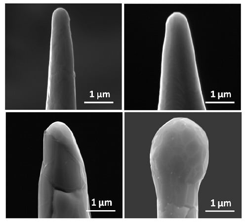
2.4. Nanoscale Point-Cathode Emitters

Nanostructures in the form of one-dimensional (1D) nanowires, nanotubes, and nanocones have attracted much attention in past decades and have been demonstrated for many potential applications. In particular, their use as electron field emitters exhibit excellent geometric, electrical and mechanical properties, as compared to conventional metallic cold field emitters [47,48,49,50]. However, there are also significant technical challenges that have yet to be resolved.
Generally, preparation of an individual nanoscopic CFE electron emitter is an extremely labor-intensive delicate process. To mount a single nanowire or nanotube onto a supporting tip, the most common method is to use microscopic manipulators under the observation of an electron microscope. Figure 2A,C show a single LaB6 nanowire [16] and a single carbon nanotube (CNT) [10] mounted on a sharpened W tip, respectively. The ends of the emitter were deposited with platinum (or carbon) by electron beam induced deposition (EBID) in order to make good electrical contact and the final emitter structure is fitted into an electron gun unit as shown in Figure 2B, and its inset. Figure 2D,E show the mounting procedure for a carbon cone nanotip (CCnT) [14], where a CCnT was welded onto the apex of the supporting tip by using a gas injecting system. The whole process has a very high probability of incurring misalignment and damage.
These nanoscale point-cathode emitters also have the limitation that they need to be operated in an UHV level, in the 10−11 to 10−10 Torr range. For a LaB6 point-cathode emitter with a diameter of nearly 60 nm, a reduced brightness (Br) value of 2.77 × 10¹¹ Am−2sr−1V−1 and an energy spread value of 0.367 eV have been reported in a vacuum with a base pressure of 10−10 Torr. The short-term stability profile of the LaB6 point-cathode is 0.32% over 60 s, and the emission current deviates from the mean within 5% throughout a week-long test. For the CNT and CCnT point-cathode emitters with diameters of around 10 nm, the source electron optics parameters were reported to be 8.2 × 10⁹ Am−2sr−1V−1, 0.48 eV, and 1.6 × 10⁹ Am−2sr−1V−1, 0.32 eV respectively. The vacuum pressure requirements are even more stringent, typically around 10−11 Torr. It was found that there exists some unrecoverable structure damage to the CNT during electron emission under the high vacuum (HV) conditions of 9 × 10⁻⁸ Torr, and this leads to emission reduction or failure [51]. In addition to its inherent UHV requirements, the CNT emitter is reported to have relatively large fluctuations in emission current, e.g., up to 24% for an emission current of about 2 µA over 6 hours with a sampling rate of 3 × 10⁻³ Hz.
These nanoscale CFE electron sources have not as yet been successfully integrated in any commercial electron microscopes due to the aforementioned significant technical challenges, and studies of nanowire, nanotube, and nanocone based cold field emitters have remained at the research level. Meanwhile, other developments in CFE electron emitter research have come from the use of materials such as graphene.

3. Graphene-Based Cold Field Emitters

Fast development of two-dimensional (2D) graphene in recent years has led to a variety of different applications for field emission based devices [20,53]. Compared with other metallic or 1D nanoscale CFE electron sources, graphene is well known for possessing several desirable properties: (1) it has excellent thermal, mechanical, and electrical characteristics [17,21]; (2) its work function can be significantly lowered both by direct contact with metals (effectively doping it), and through the application of intense electric fields [54,55]; and (3) it is extremely flexible. Graphene CFE electron sources fall into two main categories: the single-tip cathode field nano-emitter (which includes point cathodes and ring cathodes) and graphene film cathodes, which consist of densely packed graphene nano-emitters. Only the former can be used for electron microscopy applications, as the latter produces a large array of defocused overlapping electron virtual sources that cannot be subsequently focused down to a single nano-sized probe.

3.1. Graphene Film Emitters

To achieve successful electron emission from graphene, it is crucial to orientate thin graphene edges or control the dimension of graphene protrusions on some supporting substrate, in order to sufficiently enhance the applied electric field to produce quantum tunneling. Until now, many emerging technologies have become available for fabricating vertically aligned graphene nanosheets (VG) or graphene protrusions. The plasma-enhanced chemical vapor deposition (PECVD) is the most widely used way to synthesize large-scale VG graphene films [56], which offers the advantages of a lower substrate temperature and higher growth selectivity (Figure 3A). Koh et al. presented a pulsed laser deposition (PLD) method [57] to directly fabricate graphene thin film onto metal nano-sized Spindt tips by using the transformation of solid carbon deposited from a pulsed laser system at low temperature. The main drawback of these two deposition methods is the difficulty of controlling the graphene film ordering and density without incurring problems such as the screening effect [58,59].
Wu et al. applied the electrophoretic deposition (EPD) technique [60] to fabricate a large area of homogeneous single-layer graphene films, and this processing technique is more economic and versatile compared to PECVD (Figure 3B). Screen printing technology is a sophisticated technology widely used in large-scale applications coating on various substrates. A screen-printed graphene cathode was fabricated by Qian et al. [61] using high-yield graphene prepared by a modified Hummers method and a hydrazine hydrate reduction process (Figure 3C). Another efficient way to produce uniform nanometer-scale graphene protrusions is through transferring graphene onto some sharp supporting substrates (Figure 3D) [24,25,62]. However, the exfoliated graphene by using either screen printing technologies, or electrophoretic deposition, or simple transfer have been found to lead to many defects to the as-grown graphene, that degrades its physical properties [63,64,65]. For graphene film emitters, high current densities, around 23 mAcm−2, have been reported with good stability over a period of several hours [60]. Current density here, is calculated by dividing the total measured emission current by the average area on the substrate occupied by emitter sites. Although not suitable for electron microscopy applications, graphene film emitters are very useful for many non-focused electron beam applications, such as flat panel display [28,66], X-ray sources [67,68,69], etc.

3.2. Graphene Point-Cathode Field Emitters

Until now, graphene point-cathode field emitters for electron microscopy applications have been rarely studied due to the difficulties inherent in controlling graphene morphology. Tsai et al. [70] reported an idea of overlaying an ultra-thin (~1 nm) graphene flake on to a blunted tungsten probe by van der Waals forces, as shown in Figure 4A, which would make it applicable to single-column electron beam microscopy applications. However, this loosely hanging ultra-thin freestanding graphene flake is not suitable for practical applications, since the graphene can easily be damaged or detached from its supporting probe. More importantly, the emitting surface is not circular, it spans a few micrometers along one direction, and this means that it cannot subsequently be focused down to a single nanometer electron spot.
For most single-tip point field emitters, the emission current is surface sensitive and the adsorption of any gas molecules will increase the surface work function [15,72]. A high emission current under excessive applied voltage ionizes many gas molecules around the emission surface and eventually triggers a vacuum arc. Therefore, the practical use of cold field emitters in electron microscopes typically requires cathode flashing at regular intervals to remove the residual contaminant molecules. Endo et al. [73] reported that CFE electron sources can be cleaned by in situ Joule heating during the emission process in HV conditions, which is well known as a “conditioning” process in many cold field emission experiments [71,74,75]. For example, during the first and second cycle of voltage ramping up from the graphene flake overlaid on the tungsten probe (Figure 4A), the current-applied voltage characteristic presents a typical conditioning process, which is observed to deviate from the conventional FN plot. The third cycle of electron emission shows a well fitted FN plot with an emission current up to 6 µA. Similar work has been done by other researchers studying the field emission characteristics from reduced graphene oxide (Figure 4B) and carbon nanowalls, and they have obtained high emission current, around several tens of microamperes [71,76].
Recently, the research group at the National University of Singapore, led by A. Khursheed, have presented the development of a completely new type of cold field emission electron source (Figure 5A), a Graphene-Ni point cathode for electron microscopy systems [77]. They present a way of overcoming the morphological problems associated with micro-fabricating single-tip graphene emitters, by coating it on to a sharpened wire metal wire tip. In doing so, they have overcome many of the practical difficulties associated with conventional metallic tungsten CFE sources, such as misalignment, stringent vacuum requirements, and current instabilities. They reported stable field emission from a point cold field emission source that can operate in High Vacuum (HV), as opposed to stringent UHV conditions, and uses relatively large cathode-tip sizes (microns), an advantage created by their very low electric field strength requirements (0.5–1.5 V/nm) and low work function (~1.1 eV). These features enable it to provide stable and repeatable emission properties, something which is not usually associated with single point cathode cold field emission sources.
The Graphene-Ni point cathode was fabricated by a two-step process, which consists firstly of an electrochemical etching process to obtain a sharp Ni tip, and secondly, a graphene coating step of chemical vapor deposition (CVD). The Graphene-Ni point cathode for cathode tip-radius of 400 nm was shown to have a high emission current of about 5 µA under a relatively low applied electric field strength (0.5–1.5 V/nm) on the tip apex. In their study, direct ray tracing simulations of electron trajectory paths leaving the emitter surface were carried out to estimate m α and F, from which the virtual source size dv and gun brightness Br were then calculated by using Equations (2) and (3). The source brightness values range from 7 × 10⁷ Am−2sr−1V−1 to 2.51 × 10⁹ Am−2sr−1V−1 for cathode tip radii in the range of 130 nm to 800 nm. It is well known that there is a trade-off between the source brightness value and the tip size. On the one hand, a larger tip size has a greater emission area, thereby having a better current stability and can operate in much less stringent vacuum conditions [78]. One the other hand, a larger tip size has a larger virtual source size and a lower source brightness value. This trade-off is applicable to all CFE sources, and most of the previous studies on CNT, LaB6, and CCnT tips made great efforts to maximize gun brightness at the price of having poor gun current stability and stringent vacuum requirements. Another stand out feature of the Graphene-Ni point cathodes is their low energy spread (Figure 5B). The measured energy spread ranges from 0.246 eV to 0.420 eV for tip radii in the range of 260 nm to 500 nm. The Graphene-Ni point cathode as presented here appears to have overcome many of the practical engineering difficulties. A comparison of typical operating parameters and electron optical properties for the Graphene-Ni point cathode and the state-of-the-art electron sources is listed in Table 1.

3.3. Graphene Ring-Cathode Field Emitters

Khursheed first proposed the idea of using a ring-cathode emitter for combining high spatial resolution with high beam current for focused electron beam applications in 2013 [79,80]. Khursheed presented electron focused beam designs based upon using ring-cathodes together with off-axis aberration correction techniques. The first step towards a practical implementation of this idea is to develop a ring-cathode emitter. The proposal of a field emission ring-cathode gun unit has the advantage of intrinsically being a large area field emitter, and it is therefore expected to overcome the well-known disadvantage of conventional point-cathode field emitters having relatively low total current (compared to earlier larger cathode electron gun designs). The much larger emission area of a ring-cathode field emitter, compared to a point-cathode field emitter is also expected to provide it with greater current stability.
Nguyen et al. [81] reported a versatile and robust method based on graphene growth on Ni templates and thermo-assisted removal of poly(methyl methacrylate) (PMMA) for fabrication of macroscopic and freestanding tubular graphene (TG) architectures. The TG architectures have a diameter of 50 µm with a wall thickness in the range of 2.1–2.9 nm (Figure 6A). The individual TG emitter can produce an extremely high emission current, up to 0.46 mA at a very low external applied electric field of 0.68 V µm−1. This most likely comes from ultrathin edges on graphitic walls, which consist of a great number of field emission sites. Another important observation is that the TG CFE electron source has good current stability and the stability is maintainable for days under HV conditions (2.2 × 10⁻⁸ Torr). However, one limitation of TG architectures fabricated by Nguyen et al. is that the edges are very jagged rather than being smooth, making it hard to be directly used as a CFE electron source for electron microscopy applications. Moreover, transfer and alignment of such a large diameter graphene tube is an extremely delicate process.
Shao et al. [82] reported an in-situ fabrication technique, eliminating any transfer and alignment process. They obtained a graphene ring emitter, which consists of a graphene tube grown in situ on a sharp nickel wire tip (Figure 6B). The diameter of the tubular graphene is about 5 µm while the edge of the tube is approximately 2.7 nm. They have obtained high emission current of ~30 µA at the relatively low applied field of ~1.75 V/mm. The ring-cathode field emitter is a new type of field emitter source, and suitable electron ring-focused beam columns will first need to be designed for it. When that is achieved, it is expected to a wide variety of applications in subjects such as lithography, mass spectrometer, X-ray tube and accelerator physics.

4. Conclusions

High brightness, low energy spread and good current stability are critical for CFE electron sources for electron microscopy applications. Although considerable research has been carried out into developing single crystal tungsten and other 1D nanostructure-based field emitters, they have as yet, faced many practical technological difficulties, such as stringent UHV requirements, poor current stability and fast emission decay. Therefore, other ways to make CFE electron sources need to be investigated. With the fast development of 2D graphene in recent years, graphene has been proven to have ultra-high aspect ratios, good electric conductivity, chemical inertness and mechanical hardness, and these properties make graphene-based field emitters an attractive possible alternative. Three types of graphene-based field emitters have been highlighted in this review: graphene film emitters, graphene point/edge-cathode emitters, and graphene ring-cathode emitters. Most graphene field emitters proposed and studied so however, involve field emission from multiple emission sites, and are therefore not suitable for electron microscopy applications.
This paper has highlighted some recent promising developments in the category of single-point and ring-shaped graphene field emitters for electron microscopy applications, however, the investigation of graphene field emitters is still in an early stage of development, and there is still much room for further improvement. More emission characterization tests need to be performed, ones that can measure the source virtual source size, transverse coherent length, emission under a variety of different vacuum conditions, and emitter lifetime need to be made. An electron gun unit that can accommodate promising graphene emitters, which has its optical axis well aligned to the central axis of the cathode still needs to be developed. Beyond that, electron guns based upon the new class of graphene-based field emitters need to be fitted on to electron microscopes, and their performance critically compared to convention systems, in terms of parameters such as image resolution and signal-to-noise ratio.

Funding

This research was funded by National Research Foundation Singapore (NRF-CRP13-2014-04).

Acknowledgments

We acknowledge many discussions with Wei Kean Ang in the Department of Electrical and Computer Engineering, National University of Singapore. This work is funded by National Research Foundation Singapore (NRF-CRP13-2014-04).

Conflicts of Interest

The authors declare no conflict of interest.

References

  1. Dyke, W.; Dolan, W. Field emission. Adv. Electron. Electron Phys. 1956, 8, 89–185. [Google Scholar]
  2. Crewe, A.; Wall, J.; Welter, L. A high-resolution scanning transmission electron microscope. J. Appl. Phys. 1968, 39, 5861–5868. [Google Scholar] [CrossRef]
  3. Crewe, A.V.; Isaacson, M.; Johnson, D. A simple scanning electron microscope. Rev. Sci. Instrum. 1969, 40, 241–246. [Google Scholar] [CrossRef]
  4. Swanson, L.; Schwind, G. A review of the cold-field electron cathode. Adv. Imaging Electron Phys. 2009, 159, 63–100. [Google Scholar]
  5. Schwind, G.; Magera, G.; Swanson, L. Comparison of parameters for Schottky and cold field emission sources. J. Vac. Sci. Technol. B 2006, 24, 2897–2901. [Google Scholar] [CrossRef]
  6. Tuggle, D.; Swanson, L. Emission characteristics of the ZrO/W thermal field electron source. J. Vac. Sci. Technol. B 1985, 3, 220–223. [Google Scholar] [CrossRef]
  7. Fransen, M.; Overwijk, M.; Kruit, P. Brightness measurements of a ZrO/W Schottky electron emitter in a transmission electron microscope. Appl. Surf. Sci. 1999, 146, 357–362. [Google Scholar] [CrossRef]
  8. Tuggle, D.; Swanson, L.; Orloff, J. Application of a thermal field emission source for high resolution, high current e-beam microprobes. J. Vac. Sci. Technol. 1979, 16, 1699–1703. [Google Scholar] [CrossRef]
  9. Crewe, A.; Eggenberger, D.; Wall, J.; Welter, L. Electron gun using a field emission source. Rev. Sci. Instrum. 1968, 39, 576–583. [Google Scholar] [CrossRef]
  10. De Jonge, N.; Van Druten, N. Field emission from individual multiwalled carbon nanotubes prepared in an electron microscope. Ultramicroscopy 2003, 95, 85–91. [Google Scholar] [CrossRef]
  11. Bonard, J.-M.; Dean, K.A.; Coll, B.F.; Klinke, C. Field emission of individual carbon nanotubes in the scanning electron microscope. Phys. Rev. Lett. 2002, 89, 197602. [Google Scholar] [CrossRef] [PubMed]
  12. Fransen, M.; Van Rooy, T.L.; Kruit, P. Field emission energy distributions from individual multiwalled carbon nanotubes. Appl. Surf. Sci. 1999, 146, 312–327. [Google Scholar] [CrossRef]
  13. De Jonge, N.; Lamy, Y.; Schoots, K.; Oosterkamp, T.H. High brightness electron beam from a multi-walled carbon nanotube. Nature 2002, 420, 393. [Google Scholar] [CrossRef] [PubMed]
  14. Houdellier, F.; De Knoop, L.; Gatel, C.; Masseboeuf, A.; Mamishin, S.; Taniguchi, Y.; Delmas, M.; Monthioux, M.; Hÿtch, M.; Snoeck, E. Development of TEM and SEM high brightness electron guns using cold-field emission from a carbon nanotip. Ultramicroscopy 2015, 151, 107–115. [Google Scholar] [CrossRef] [PubMed]
  15. Yeong, K.; Thong, J. Field-emission properties of ultrathin 5 nm tungsten nanowire. J. Appl. Phys. 2006, 100, 114325. [Google Scholar] [CrossRef]
  16. Zhang, H.; Tang, J.; Yuan, J.; Yamauchi, Y.; Suzuki, T.T.; Shinya, N.; Nakajima, K.; Qin, L.-C. An ultrabright and monochromatic electron point source made of a LaB6 nanowire. Nat. Nanotechnol. 2016, 11, 273. [Google Scholar] [CrossRef] [PubMed]
  17. Novoselov, K.S.; Geim, A.K.; Morozov, S.; Jiang, D.; Katsnelson, M.; Grigorieva, I.; Dubonos, S.; Firsov, A.A. Two-dimensional gas of massless Dirac fermions in graphene. Nature 2005, 438, 197–200. [Google Scholar] [CrossRef] [PubMed] [Green Version]
  18. Xiao, Z.; She, J.; Deng, S.; Tang, Z.; Li, Z.; Lu, J.; Xu, N. Field electron emission characteristics and physical mechanism of individual single-layer graphene. ACS Nano 2010, 4, 6332–6336. [Google Scholar] [CrossRef] [PubMed]
  19. Lei, W.; Li, C.; Cole, M.T.; Qu, K.; Ding, S.; Zhang, Y.; Warner, J.H.; Zhang, X.; Wang, B.; Milne, W.I. A graphene-based large area surface-conduction electron emission display. Carbon 2013, 56, 255–263. [Google Scholar] [CrossRef]
  20. Geim, A.K.; Novoselov, K.S. The rise of graphene. Nat. Mater. 2007, 6, 183–191. [Google Scholar] [CrossRef] [PubMed]
  21. Balandin, A.A.; Ghosh, S.; Bao, W.; Calizo, I.; Teweldebrhan, D.; Miao, F.; Lau, C.N. Superior thermal conductivity of single-layer graphene. Nano Lett. 2008, 8, 902–907. [Google Scholar] [CrossRef] [PubMed]
  22. Neto, A.C.; Guinea, F.; Peres, N.M.; Novoselov, K.S.; Geim, A.K. The electronic properties of graphene. Rev. Mod. Phys. 2009, 81, 109. [Google Scholar] [CrossRef]
  23. Lee, C.; Wei, X.; Kysar, J.W.; Hone, J. Measurement of the elastic properties and intrinsic strength of monolayer graphene. Science 2008, 321, 385–388. [Google Scholar] [CrossRef] [PubMed]
  24. Ye, D.; Moussa, S.; Ferguson, J.D.; Baski, A.A.; El-Shall, M.S. Highly efficient electron field emission from graphene oxide sheets supported by nickel nanotip arrays. Nano Lett. 2012, 12, 1265–1268. [Google Scholar] [CrossRef] [PubMed]
  25. Lv, S.; Li, Z.; Liao, J.; Wang, G.; Li, M.; Miao, W. Optimizing field emission properties of the hybrid structures of graphene stretched on patterned and size-controllable SiNWs. Sci. Rep. 2015, 5, 15035. [Google Scholar] [CrossRef] [PubMed]
  26. Zhang, Y.; Du, J.; Tang, S.; Liu, P.; Deng, S.; Chen, J.; Xu, N. Optimize the field emission character of a vertical few-layer graphene sheet by manipulating the morphology. Nanotechnology 2011, 23, 015202. [Google Scholar] [CrossRef] [PubMed]
  27. Hernandez-Garcia, C.; O Shea, P.G.; Stutzman, M.L. Electron sources for accelerators. Phys. Today 2008, 61, 44–49. [Google Scholar] [CrossRef]
  28. Choi, W.; Chung, D.; Kang, J.; Kim, H.; Jin, Y.; Han, I.; Lee, Y.; Jung, J.; Lee, N.; Park, G. Fully sealed, high-brightness carbon-nanotube field-emission display. Appl. Phys. Lett. 1999, 75, 3129–3131. [Google Scholar] [CrossRef]
  29. Saito, Y.; Uemura, S. Field emission from carbon nanotubes and its application to electron sources. Carbon 2000, 38, 169–182. [Google Scholar] [CrossRef]
  30. Barber, M.; Bordoli, R.; Sedgwick, R.; Tyler, A. Fast atom bombardment of solids as an ion source in mass spectrometry. Nature 1981, 293, 270–275. [Google Scholar] [CrossRef]
  31. Khursheed, A. Scanning Electron Microscope. U.S. Patent 7,294,834, 2007. [Google Scholar]
  32. Khursheed, A. Scanning Electron Microscope Optics and Spectrometers; World Scientific: Singapore, 2011. [Google Scholar]
  33. Murphy, E.L.; Good, R., Jr. Thermionic emission, field emission, and the transition region. Phys. Rev. 1956, 102, 1464. [Google Scholar] [CrossRef]
  34. Fowler, R.H.; Nordheim, L. Electron emission in intense electric fields. Proc. R. Soc. Lond. A 1928, 119, 173–181. [Google Scholar] [CrossRef]
  35. Bronsgeest, M.; Barth, J.; Swanson, L.; Kruit, P. Probe current, probe size, and the practical brightness for probe forming systems. J. Vac. Sci. Technol. B 2008, 26, 949–955. [Google Scholar] [CrossRef]
  36. Kruit, P.; Jansen, G.H. Space charge and statistical coulomb effects. In Handbook of Charged Particle Optics, 2nd ed.; Taylor & Francis: Abingdon, UK, 1997. [Google Scholar]
  37. Cook, B.; Verduin, T.; Hagen, C.; Kruit, P. Brightness limitations of cold field emitters caused by Coulomb interactions. J. Vac. Sci. Technol. B 2010, 28. [Google Scholar] [CrossRef]
  38. Kratschmer, E.; Rishton, S.; Kern, D.; Chang, T. Quantitative analysis of resolution and stability in nanometer electron beam lithography. J. Vac. Sci. Technol. B 1988, 6, 2074–2079. [Google Scholar] [CrossRef]
  39. Rishton, S.; Beaumont, S.; Wilkinson, C. Measurement of the profile of finely focused electron beams in a scanning electron microscope. J. Phys. E Sci. Instrum. 1984, 17, 296. [Google Scholar] [CrossRef]
  40. Fransen, M.; Damen, E.; Schiller, C.; van Rooy, T.; Groen, H.; Kruit, P. Characterization of ultrasharp field emitters by projection microscopy. Appl. Surf. Sci. 1996, 94, 107–112. [Google Scholar] [CrossRef]
  41. Young, R.D. Theoretical total-energy distribution of field-emitted electrons. Phys. Rev. 1959, 113, 110. [Google Scholar] [CrossRef]
  42. Knauer, W. Energy broadening in field emitted electron and ion-beams. Optik 1981, 59, 335–354. [Google Scholar]
  43. Krivanek, O.; Corbin, G.; Dellby, N.; Elston, B.; Keyse, R.; Murfitt, M.; Own, C.; Szilagyi, Z.; Woodruff, J. An electron microscope for the aberration-corrected era. Ultramicroscopy 2008, 108, 179–195. [Google Scholar] [CrossRef] [PubMed]
  44. Jeol USA Press Releases. Available online: http://www.webcitation.org/6zUwGhedE (accessed on 18 May 2018).
  45. Dyke, W.; Charbonnier, F.; Strayer, R.; Floyd, R.; Barbour, J.; Trolan, J. Electrical stability and life of the heated field emission cathode. J. Appl. Phys. 1960, 31, 790–805. [Google Scholar] [CrossRef]
  46. Knápek, A.; Grmela, L.; Šikula, J.; Šik, O. Cold field-emission cathode noise analysis. Metrol. Meas. Syst. 2012, 19, 417–422. [Google Scholar] [CrossRef]
  47. Ajayan, P. Nanotubes from carbon. Chem. Rev. 1999, 99, 1787–1800. [Google Scholar] [CrossRef] [PubMed]
  48. Berber, S.; Kwon, Y.-K.; Tománek, D. Unusually high thermal conductivity of carbon nanotubes. Phys. Rev. Lett. 2000, 84, 4613. [Google Scholar] [CrossRef] [PubMed]
  49. Ebbesen, T.; Lezec, H.; Hiura, H.; Bennett, J.; Ghaemi, H.; Thio, T. Electrical conductivity of individual carbon nanotubes. Nature 1996, 382, 54–56. [Google Scholar] [CrossRef]
  50. Zhang, H.; Tang, J.; Zhang, Q.; Zhao, G.; Yang, G.; Zhang, J.; Zhou, O.; Qin, L.C. Field emission of electrons from single LaB6 nanowires. Adv. Mater. 2006, 18, 87–91. [Google Scholar] [CrossRef]
  51. Jin, C.; Wang, J.; Wang, M.; Su, J.; Peng, L.-M. In-Situ studies of electron field emission of single carbon nanotubes inside the tem. Carbon 2005, 43, 1026–1031. [Google Scholar] [CrossRef]
  52. Houdellier, F.; Masseboeuf, A.; Monthioux, M.; Hÿtch, M.J. New carbon cone nanotip for use in a highly coherent cold field emission electron microscope. Carbon 2012, 50, 2037–2044. [Google Scholar] [CrossRef]
  53. Knápek, A.; Sobola, D.; Tománek, P.; Pokorná, Z.; Urbánek, M. Field emission from the surface of highly ordered pyrolytic graphite. Appl. Surf. Sci. 2017, 395, 157–161. [Google Scholar] [CrossRef]
  54. Giovannetti, G.; Khomyakov, P.; Brocks, G.; Karpan, V.V.; Van den Brink, J.; Kelly, P.J. Doping graphene with metal contacts. Phys. Rev. Lett. 2008, 101, 026803. [Google Scholar] [CrossRef] [PubMed]
  55. Kwon, K.C.; Choi, K.S.; Kim, B.J.; Lee, J.-L.; Kim, S.Y. Work-function decrease of graphene sheet using alkali metal carbonates. J. Phys. Chem. C 2012, 116, 26586–26591. [Google Scholar] [CrossRef]
  56. Malesevic, A.; Kemps, R.; Vanhulsel, A.; Chowdhury, M.P.; Volodin, A.; Van Haesendonck, C. Field emission from vertically aligned few-layer graphene. J. Appl. Phys. 2008, 104, 084301. [Google Scholar] [CrossRef]
  57. Koh, A.T.; Foong, Y.M.; Yusop, Z.; Tanemura, M.; Chua, D.H. Low temperature direct of graphene onto metal nano-spindt tip with applications in electron emission. Adv. Mater. Interfaces 2014, 1. [Google Scholar] [CrossRef]
  58. Suh, J.S.; Jeong, K.S.; Lee, J.S.; Han, I. Study of the field-screening effect of highly ordered carbon nanotube arrays. Appl. Phys. Lett. 2002, 80, 2392–2394. [Google Scholar] [CrossRef]
  59. Bonard, J.M.; Weiss, N.; Kind, H.; Stöckli, T.; Forró, L.S.; Kern, K.; Chatelain, A. Tuning the field emission properties of patterned carbon nanotube films. Adv. Mater. 2001, 13, 184–188. [Google Scholar] [CrossRef]
  60. Wu, Z.S.; Pei, S.; Ren, W.; Tang, D.; Gao, L.; Liu, B.; Li, F.; Liu, C.; Cheng, H.M. Field emission of single-layer graphene films prepared by electrophoretic deposition. Adv. Mater. 2009, 21, 1756–1760. [Google Scholar] [CrossRef]
  61. Qian, M.; Feng, T.; Ding, H.; Lin, L.; Li, H.; Chen, Y.; Sun, Z. Electron field emission from screen-printed graphene films. Nanotechnology 2009, 20, 425702. [Google Scholar] [CrossRef] [PubMed]
  62. Hwang, J.O.; Lee, D.H.; Kim, J.Y.; Han, T.H.; Kim, B.H.; Park, M.; No, K.; Kim, S.O. Vertical ZnO nanowires/graphene hybrids for transparent and flexible field emission. J. Mater. Chem. 2011, 21, 3432–3437. [Google Scholar] [CrossRef]
  63. Hallam, T.; Berner, N.C.; Yim, C.; Duesberg, G.S. Strain, bubbles, dirt, and folds: A study of graphene polymer-assisted transfer. Adv. Mater. Interfaces 2014, 1. [Google Scholar] [CrossRef]
  64. Li, X.; Zhu, Y.; Cai, W.; Borysiak, M.; Han, B.; Chen, D.; Piner, R.D.; Colombo, L.; Ruoff, R.S. Transfer of large-area graphene films for high-performance transparent conductive electrodes. Nano Lett. 2009, 9, 4359–4363. [Google Scholar] [CrossRef] [PubMed]
  65. Suk, J.W.; Kitt, A.; Magnuson, C.W.; Hao, Y.; Ahmed, S.; An, J.; Swan, A.K.; Goldberg, B.B.; Ruoff, R.S. Transfer of CVD-grown monolayer graphene onto arbitrary substrates. ACS Nano 2011, 5, 6916–6924. [Google Scholar] [CrossRef] [PubMed]
  66. Yang, C.; Liu, N.; Zeng, W.; Long, F.; Song, Z.; Su, J.; Li, L.; Zou, Z.; Fang, G.; Xiong, L. Superelastic and ultralight electron source from modifying 3D reduced graphene aerogel microstructure. Nano Energy 2017, 33, 280–287. [Google Scholar] [CrossRef]
  67. Lee, H.R.; Lee, S.W.; Shikili, C.; Kang, J.S.; Lee, J.; Park, K.C. Enhanced electron emission of paste CNT emitters with nickel buffer layer and its X-ray application. J. Nanosci. Nanotechnol. 2016, 16, 12053–12058. [Google Scholar] [CrossRef]
  68. Sugie, H.; Tanemura, M.; Filip, V.; Iwata, K.; Takahashi, K.; Okuyama, F. Carbon nanotubes as electron source in an X-ray tube. Appl. Phys. Lett. 2001, 78, 2578–2580. [Google Scholar] [CrossRef]
  69. Lee, Y.Z.; Burk, L.; Wang, K.-H.; Cao, G.; Lu, J.; Zhou, O. Carbon nanotube based X-ray sources: Applications in pre-clinical and medical imaging. Nucl. Instrum. Meth. A 2011, 648, S281–S283. [Google Scholar] [CrossRef] [PubMed]
  70. Tsai, J.T.; Chu, T.Y.; Shiu, J.Y.; Yang, C.S. Field emission from an individual freestanding graphene edge. Small 2012, 8, 3739–3745. [Google Scholar] [CrossRef] [PubMed]
  71. Yamaguchi, H.; Murakami, K.; Eda, G.; Fujita, T.; Guan, P.; Wang, W.; Gong, C.; Boisse, J.; Miller, S.; Acik, M. Field emission from atomically thin edges of reduced graphene oxide. ACS Nano 2011, 5, 4945–4952. [Google Scholar] [CrossRef] [PubMed]
  72. Kleint, C. Electron emission noise. Surf. Sci. 1988, 200, 472–489. [Google Scholar] [CrossRef]
  73. Endo, Y.; Honjo, I.; Goto, S. Microelectron gun with silicon field emitter. J. Vac. Sci. Technol. B 1998, 16, 3082–3085. [Google Scholar] [CrossRef]
  74. Purcell, S.; Vincent, P.; Journet, C.; Binh, V.T. Hot nanotubes: Stable heating of individual multiwall carbon nanotubes to 2000 K induced by the field-emission current. Phys. Rev. Lett. 2002, 88, 105502. [Google Scholar] [CrossRef] [PubMed]
  75. Semet, V.; Binh, V.T.; Vincent, P.; Guillot, D.; Teo, K.; Chhowalla, M.; Amaratunga, G.; Milne, W.; Legagneux, P.; Pribat, D. Field electron emission from individual carbon nanotubes of a vertically aligned array. Appl. Phys. Lett. 2002, 81, 343–345. [Google Scholar] [CrossRef]
  76. Wang, Y.; Yang, Y.; Zhao, Z.; Zhang, C.; Wu, Y. Local electron field emission study of two-dimensional carbon. Appl. Phys. Lett. 2013, 103, 033115. [Google Scholar] [CrossRef]
  77. Shao, X.; Srinivasan, A.; Ang, W.K.; Khursheed, A. A high-brightness large-diameter graphene coated point cathode field emission electron source. Nat. Commun. 2018, 9, 1288. [Google Scholar] [CrossRef] [PubMed]
  78. Swanson, L.; Martin, N. Field electron cathode stability studies: Zirconium/tungsten thermal-field cathode. J. Appl. Phys. 1975, 46, 2029–2050. [Google Scholar] [CrossRef]
  79. Khursheed, A. Design of a focused electron beam column for ring-cathode sources. Ultramicroscopy 2013, 128, 10–23. [Google Scholar] [CrossRef] [PubMed]
  80. Khursheed, A.; Ang, W.K. Annular focused electron/ion beams for combining high spatial resolution with high probe current. Microsc. Microanal. 2016, 22, 948–954. [Google Scholar] [CrossRef] [PubMed]
  81. Nguyen, D.D.; Suzuki, S.; Kato, S.; To, B.D.; Hsu, C.C.; Murata, H.; Rokuta, E.; Tai, N.-H.; Yoshimura, M. Macroscopic, freestanding, and tubular graphene architectures fabricated via thermal annealing. ACS Nano 2015, 9, 3206–3214. [Google Scholar] [CrossRef] [PubMed]
  82. Shao, X.; Srinivasan, A.; Zhao, Y.; Khursheed, A. A few-layer graphene ring-cathode field emitter for focused electron/ion beam applications. Carbon 2016, 110, 378–383. [Google Scholar] [CrossRef]
Figure 1. Scanning electron microscopy (SEM) photos of the W<310> (A) and W<111> (B) cold field emission (CFE) sources; (C) The source reduced brightness Br versus the corresponding Full width at half maximum (FWHM(E)) values for the two CFE sources. Reproduced with permission from [4], Copyright Elsevier, 2009.
Applsci 08 00868 g001
Figure 2. Well-developed nanowire, nanotube, and nanocone point-cathode cold field emitters. (A) Illustration showing the electron beam deposition process to fix a LaB6 nanowire onto a W needle; (B) SEM image showing the finished LaB6 NW emitter and the complete emitter assembly used for field-emission SEM, scale bar, 10 µm. Reproduced with permission from [16], Copyright Springer Nature, 2015; (C) Transmission electron microscopy (TEM) image of a very thin and short nanotube sample. Reproduced with permission from [10], Copyright Elsevier, 2003; (D) View of part of the starting carbon cone nanotip (CCnT) object; (E) Resulting new tip after welding the carbon microfiber to the tungsten tip. The inset displays the whole set-up inside the dual beam. Reproduced with permission from [52], Copyright Elsevier, 2012.
Applsci 08 00868 g002
Figure 3. SEM images of microfabricated graphene film emitters. (A) Top view SEM micrograph of as grown few-layer graphene (FLG) by microwave plasma-enhanced chemical vapor deposition (PECVD). Reproduced with permission from [56], Copyright AIP, 2008; (B) Graphene films prepared by electrophoretic deposition. Reproduced with permission from [60], Copyright Wiley, 2009; (C) Screen-printed graphene films. Reproduced with permission from [61], Copyright IOP, 2009; (D) Hybrid structures of graphene stretched on patterned and size-controllable Si nanowires. Reproduced with permission from [25], Copyright Springer Nature, 2015. ITO: indium tin oxide; PMMA: poly(methyl methacrylate).
Applsci 08 00868 g003
Figure 4. Images of graphene edge field emitters and field emission characteristics. (A) Field emission from individual freestanding graphene edge. Reproduced with permission from [70], Copyright Wiley, 2013; (B) Field emission from atomically thin edges of reduced graphene oxide. Reproduced with permission from [71], Copyright American Chemical Society (ACS) publications, 2011.
Applsci 08 00868 g004
Figure 5. Graphene-coated point cathode field emitter. (A) SEM images of graphene-coated point cathode emitter. Reproduced with permission from [77], Copyright Springer Nature, 2018; (B) Source brightness and energy spread. Reproduced with permission from [77], Copyright Springer Nature, 2018. CVD: chemical vapor deposition.
Applsci 08 00868 g005
Figure 6. Graphene ring-cathode field emitter. (A) Macroscopic, freestanding, and tubular graphene architectures. Reproduced with permission from [81], Copyright ACS publications, 2015; (B) A few-layer graphene ring-cathode field emitter. Reproduced with permission from [82], Copyright Elsevier, 2016.
Applsci 08 00868 g006
Table 1. Comparison of typical operating parameters and electron optical properties for the graphene coated point cathode and the state-of-the-art electron sources.
VacuumWork Function (eV)Chemical InertnessBrightness (A/m2srV)Energy Spread (eV)Current StabilityRef.
Applsci 08 00868 i001UHV, XHV4.5No~1090.2–0.37.2% (UHV)[4,16]
Applsci 08 00868 i002Less stringent UHV2.8No~1080.5–0.80.23–3.1%[5,16]
Applsci 08 00868 i003HV1.1YesFor 175 nm ~109
For 800 nm ~108
0.2–0.45–10% (HV)[77]
UHV: ultra-high vacuum; XHV: extreme high vacuum.

