Article

Design of Three Phase Solid State Transformer Deployed within Multi-Stage Power Switching Converters

1
Electrical Engineering Department, The University of Lahore, Lahore 54000, Pakistan
2
Faculty of Engineering, “Aurel Vlaicu” University of Arad, Arad 310130, Romania
3
Automatics and Applied Software Department, “Aurel Vlaicu” University of Arad, Arad 310130, Romania
4
Electrical and Computer Engineering Department, Dalhousie University, Halifax, NS B3H 4R2, Canada
5
Electrical Engineering Department, University of the Punjab Lahore, Lahore 54590, Pakistan
*
Author to whom correspondence should be addressed.
Appl. Sci. 2019, 9(17), 3545; https://doi.org/10.3390/app9173545
Submission received: 25 July 2019 / Revised: 21 August 2019 / Accepted: 24 August 2019 / Published: 29 August 2019
(This article belongs to the Section Electrical, Electronics and Communications Engineering)

Abstract

:
This paper presents a symmetrical topology for the design of solid-state transformer; made up of power switching converters; to replace conventional bulky transformers. The proposed circuitry not only reduces the overall size but also provides power flow control with the ability to be interfaced with renewable energy resources (RESs) to fulfill the future grid requirements at consumer end. The proposed solid-state transformer provides bidirectional power flow with variable voltage and frequency operation and has the ability to maintain unity power factor; and total harmonic distortion (THD) of current for any type of load within defined limits of Institute of Electrical and Electronics Engineers (IEEE) standard. Solid state transformer offers much smaller size compared to the conventional iron core transformer. MATLAB/Simulink platform is adopted to test the validity of the proposed circuit for different scenarios by providing the simulation results evaluated at 25 kHz switching frequency.

1. Introduction

The main consideration, currently, is to supply a cheap, clean and sustainable supply of power to end consumers in the future. To meet this goal, the most significant and required change is the design of the distribution transformer. Traditional transformers are heavy, occupy a large volume and possess fix voltage and frequency operation. Traditional transformers are sensitive to transients, voltage disturbances, harmonics and inter harmonics due to non-linear and unbalanced loads [1,2]. This creates power quality issues, as effects of the load from consumer side travel to the power distribution network. Distribution transformers have a poor transformer utilization factor as the magnetic core saturates due to the harmonic nature of the load. The presence of harmonic current due to nonlinear and unbalanced loads also influences the primary side current, thus creating power quality issues [3]. Besides power quality improvement and a continuous supply of power to the customers, an advanced type of transformer needs to be introduced to cope with the future grid requirement.
Over the past decade, power electronic converters have played a vital role in the well-known high voltage direct current transmission (HVDC) and flexible alternating current transmission (FACT) systems in the form of static volt ampere reactive (VAR) compensators (SVCs), static synchronous compensators (STATCOMs) and unified power flow controllers (UPFCs) and so on [4]. Since renewable energy resources (RESs) such as wind, fuel cells and solar have penetrated into the industry, so power electronic converters also find their applications in them [5,6]. Energy resources like natural coal or gas are limited and the use of RESs is growing constantly with the aim to exchange electric power with the grid by net metering. Owing to the fact that the conventional transformer cannot be interfaced with RESs and the progress made in the field of power electronics, have led to the evolution of another power electronic converter named the solid state transformer, also known as the power electronic transformer, that has gained a lot of attention [7,8,9,10,11].
With the progress made in the field of the semiconductor industry, high-frequency controlled switches with high-power ratings have been developed. With these advancements and to cope with the future requirement of distributed energy sources integration, research is being carried out in the field of power electronics, which targets the use of solid state transformers (SSTs) in applications of a high-power level. One of the key interests of researchers is to develop a dynamic architecture of SST acquiring minimum controlled switches; the other approach is the integration of SSTs with RESs and other power applications.
Solid state transformers respond to control signals but their designs are not simple due to the presence of power electronic converters. The basic principle of operation of SST is that it first transforms low-frequency (50 Hz) AC voltage to high-frequency (frequency more than 20 kHz) voltage. After that isolated dual active DC–DC high frequency converter regulates secondary direct current (DC) voltage, whose size is much smaller because of high frequency operation. The multi-stage power electronic converters use controlled power electronic switches in series. In the first stage active rectifier is used, which converts and controls grid voltage to DC grid voltage and provides extended control of active and reactive power [12]. Thus, it provides the control of power and power factor. One of the most important benefits provided by SST is that it isolates both the primary and secondary side, thus eliminating the coupling effects. Ride through capabilities, and compatibility between RESs and the grid make SST superior to conventional transformers [12]. The ability of SST to generate any variable frequency and voltage enables it to perform better and be efficient in industry applications as it removes the requirement of using variable frequency drives (VFDs). SSTs, in future, will not only replace the conventional bulky transformers dominating at charge stations, locomotive and traction applications, smart grids and at secondary distribution sides, but also provide additional functions, such as the control of the active-reactive power and distribution source integration. Reduced-volume SST with aforementioned features also plays a key role in improving the power quality [13,14].
Various two-level and multilevel switching converter topologies can be employed in SSTs as discussed in [15]. Some recent configurations of SST are also reported in [16,17,18,19]. SSTs in the form of direct Alternating Current (AC) to AC matrix converters directly convert three-phase alternating current to three phase alternating voltage [20]. SSTs without a DC link are impossible to be interfaced with RESs and fuel cells [21]. However, SST with a DC link [22] offers advantages such as the availability of DC port, and much reduced size due to high frequency operation over [20,21]. However, all aforementioned topologies involve a large number of converter valves. The isolated type topology, presented in this paper, involves the least possible number of controlled switches, completely isolates the grid from load, and provides independent control of the voltage, frequency, power flow and power factor. A very few instances (no instance, in fact) in the literature are reported where such a kind of topology can accomplish all the above-mentioned tasks. This justifies the applicability and validation of the proposed research. The suggested topology of SST also can maintain a clean voltage and current waveforms of utility supply irrespective of the type and nature of the load. This is what that has been stressed upon in this paper.
The paper is constructed in the following way. Section 2 pinpoints the proposed SST circuit topology, specifications and complete control layout. In Section 3, detailed simulation results are presented to investigate the role of SST as a variable frequency drive, power factor improvement device and renewable interface with bidirectional power flow. An active power flow mechanism with balanced and unbalanced load is also simulated in this section. Conclusions are drawn in Section 4.

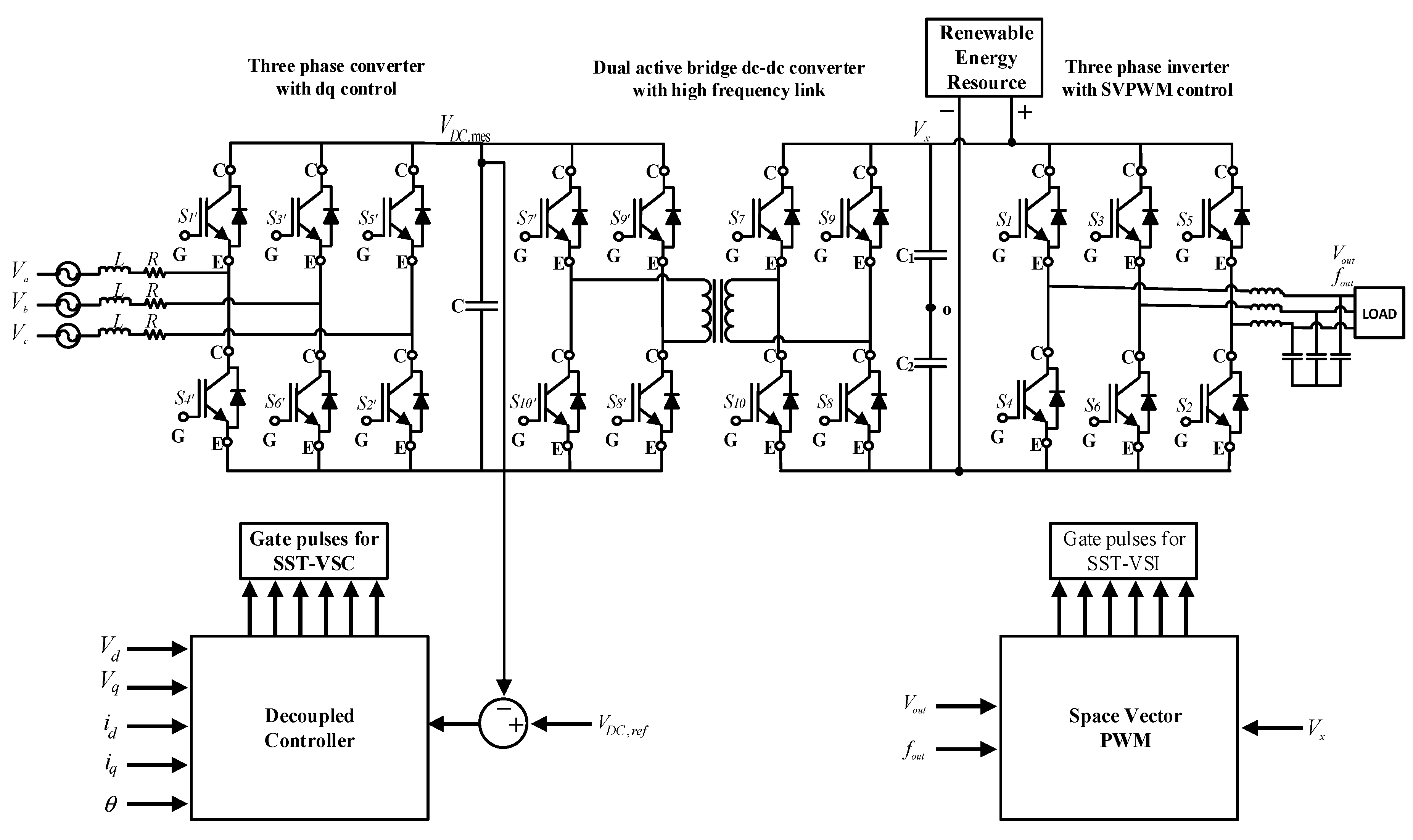
2. Proposed SST Circuit, Specifications and Control Layout

Vector control (decoupled controller) was used for a three-phase rectification purpose. Vector control employing controlled switches such as insulated gate bipolar junction transistors (IGBTs) maintains total harmonic distortion (THD) of the input current within IEEE defined limits and provides a ripple free DC output voltage. Obtained DC voltage V D C , m e s was converted to a high frequency square wave using a full-bridge inverter, which was stepped down using a ferrite core high frequency transformer. This stepped down voltage was rectified again with the help of a full-bridge converter as shown in Figure 1. In the last stage, DC voltage V x was converted back to the variable three-phase voltage with frequency and voltage control using the space vector pulse width modulation (SVPWM) technique.

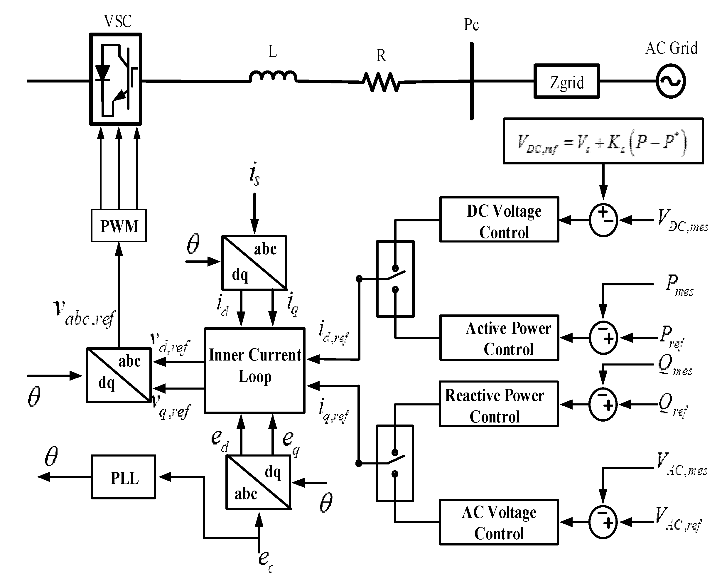
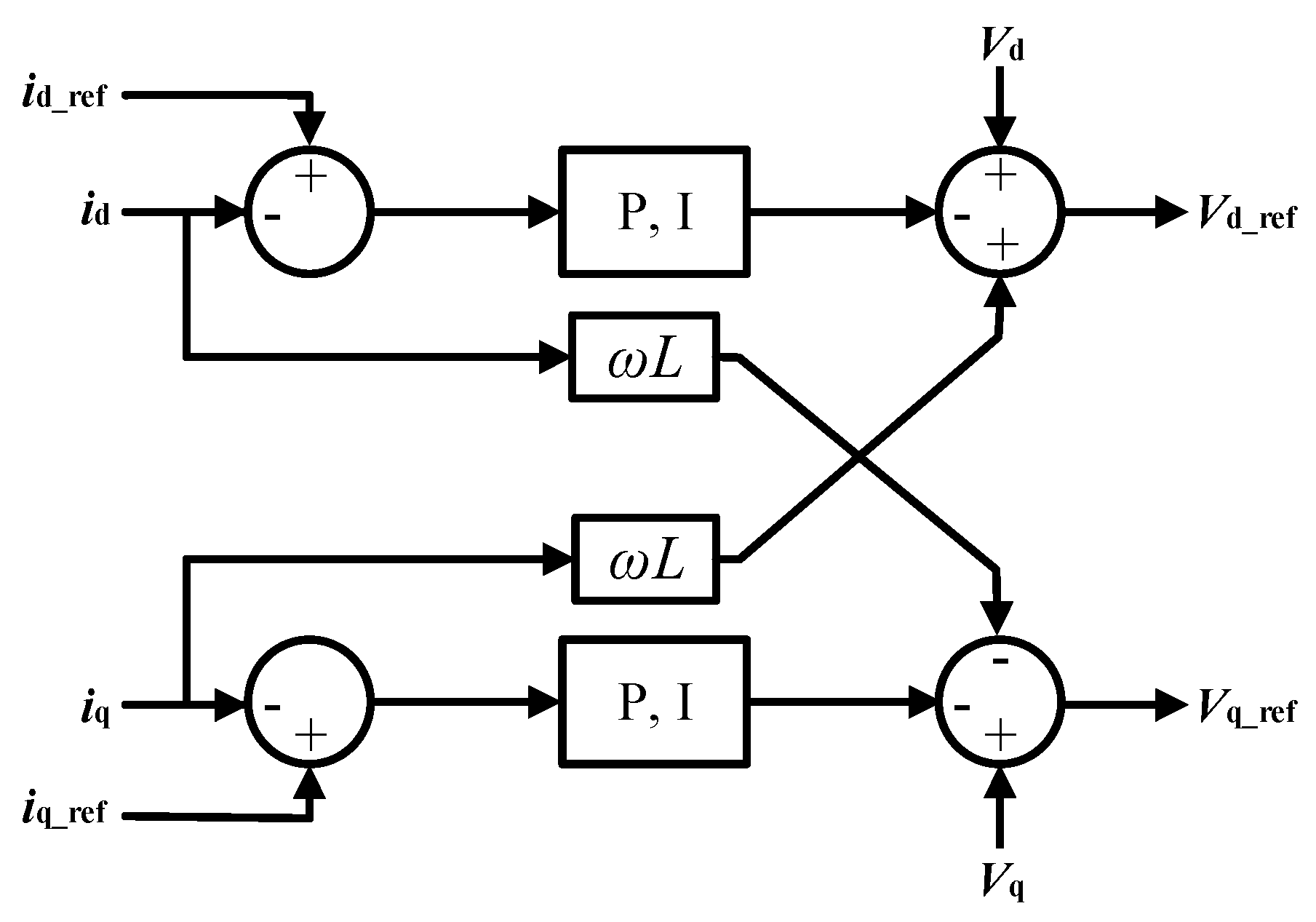
2.1. Control Layout of the SST-Voltage Source Convereter

Flux-oriented vector current control (VOC), based on two control layers: Outer current control layer (OCC) and inner current control layer (ICC), was used to control the operation of voltage source converters (VSCs) [23]. The outer layer satisfied the DC voltage, active power and reactive power demands of the VSCs while the inner layer used the decoupling control method to regulate the q-axis and d-axis currents. Both control loops had a proportional and integral (PI) controller as a common element in them. DC link voltage V D C , m e s was regulated using the voltage droop control [24]. Through the investigation of the bi-layer control architecture deployed within a multi-input multi-output (MIMO) voltage source converter, it can be realized that the operation of SST-VSC becomes a bit complex [25]. This complex control architecture has many variables, which need to be controlled precisely using PI controllers [26]. Therefore, it is the requirement of the system that PI controllers should be optimally tuned to provide both transient and steady state desired responses. However, tuning PI parameters of the nonlinear system like the voltage source converter, is a challenging task within itself [27].
Vector current control was used at the point of common coupling, which regulates the DC voltage control at VSC and power flow control with ac voltage regulation [28]. In this technique, ac voltage and current of the VSC were converted into a rotating d–q reference frame, which was synchronized with ac grid voltages using a phase locked loop (PLL). This methodology not only regulated DC and ac voltage but also provided the decoupled control of both active and reactive power. The layout of the d–q control architecture-based SST-VSC is shown in Figure 2. The outer control loop produced reference currents for the inner current loop, which then provided the reference voltage for the d–q reference frame.
By taking the d–q control frame into consideration, the internal control loop used the PI controllers, which generated the reference current and maintained the required voltage for the VSCs. Voltage expression at the point of common coupling (pc) and the voltage source converter side (vs) can be given as:
e C v S = R × i S + L d i S d t ,
where R and L represent the resistance and inductance between SST-VSC and point of common coupling (PCC), while i S is the current from the grid to the SST-VSC.
From Park’s transformation:
e d v d = R i d ω L i q + L d i d d t .
e q v q = R i q + ω L i d + L d i q d t .
Here ω represents the angular frequency at the PCC of ac system. Based on (2) and (3), the ICC control layout is shown in Figure 3. The reference signals ( V d _ r e f and V q _ r e f ) were transformed back to the abc frame, which were used to generate switching pulses for IGBTs of VSC.
In this research, the classical tuning method was used to tune the PI controller parameters. The transfer function of the simple PI controller is:
F ( s ) = k p + k i s .
According to internal model control (IMC) method as presented in [29], we can write:
F ( s ) = k p + α I C C s G 1 ( s ) = α I C C s ( R + s L ) .
F ( s ) = α I C C L + α I C C R s .
Here α I C C (rad/s) represents the bandwidth of the current controlled system; G ( s ) is the estimation of G ( s ) . Comparison of (4) and (5) yields the range of PI controller coefficients for ICC as:
k p , I C C α I C C L .
k i , I C C α I C C R .
The bandwidth α I C C for the ICC must be selected such that it is ten times lesser than the switching frequency [30,31]. That is to say:
α I C C 2 π F s 10 .
The PI controller parameters for the OCC can also be tuned using the same procedure as for ICC but with a constraint that OCC must be ten times slower than the ICC to achieve the non-oscillatory response of the closed loop system. This is achieved by selecting the bandwidth of the OCC such that it is 10 times smaller than the bandwidth of the ICC. As presented in [32], the OCC PI controller parameters are given as:
k p , O C C α O C C C .
k i , O C C α O C C 2 C .
α O C C α I C C 10 .
The outer control loop is responsible for controlling the ac and DC voltage, both active and reactive powers at PCC. As shown in Figure 2, d-channel controlled the DC link voltage or active power control, while the q-channel regulated the ac voltage or controlled the reactive power. These relations are mathematically represented as:
P = V d i d + V q i q .
Q = V q i d V d i q .
Using PLL, the d-axis of vector control was synchronized with the phasor voltage of the ac system, so, V q = 0 . This reduced (12) and (13) to:
P = V d i d .
Q = V d i q .
From (14) and (15), the active power and reactive power is regulated by controlling the d–q axis currents. At PCC, ac voltage is regulated by the q-axis current or can also be controlled by injecting the required reactive power to the system. Likewise, the DC link voltage is maintained via the exchange of real power with an ac system or by modifying the d-axis current.
The specifications of the VSC used within SST are given in Table 1:

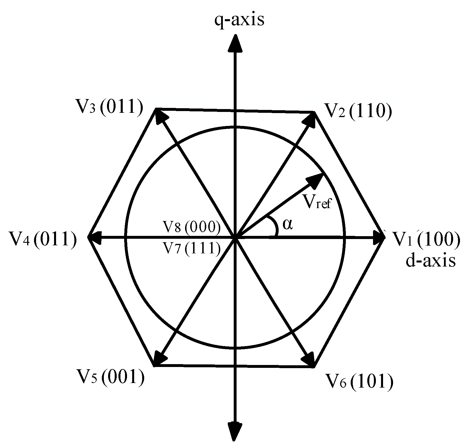
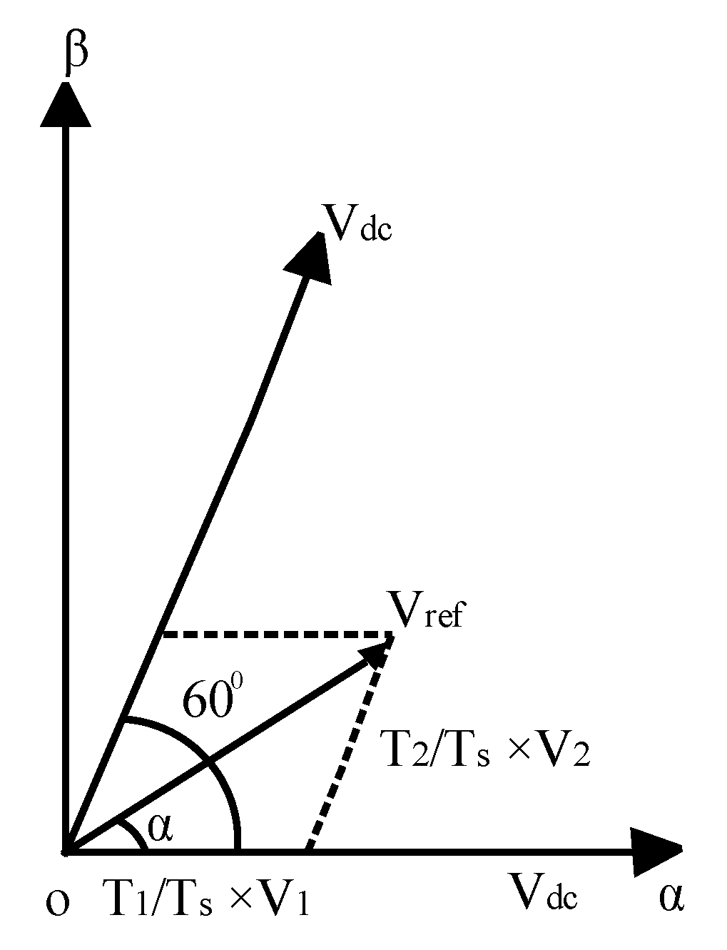
2.2. Control Layout of the SST-Voltage Source Inverter

Three phase two level voltage source inverters (VSIs), consisting of two power electronic switches in each leg, have penetrated in the industry as they provide various speed control demands of induction motor drives. A two level VSI has six active states and two null states. Various PWM techniques are proposed in [33,34] to reduce the VSI output waveform distortions at a given switching frequency. The most popular one is the space vector PWM as it provides low output current ripple and provides maximum utilization of the DC -link voltages [35,36]. It provides 15% higher ac voltage, lower current and voltage harmonics distortions as compared to conventional PWM [37]. This is the reason that SVPWM as a modulation technique is employed in this research. The active states divide the space vector plane into six sectors of equal magnitude as shown in Figure 4. Switching states for all eight (six active and two null) vectors are shown in Table 2.
Using SVPWM, desired three phase voltages are provided by the voltage vector controlled in the d–q rotating frame as shown in Figure 4, whose rotation is sampled in every sub-cycle Ts. Figure 5 shows the component of the reference voltage vector of magnitude Vref along the α and β-axis in sector I whereas, T1, T2 and Tz are dwell times for which the active voltage vector V1, active voltage vector V2 and null vectors are applied in a sub-cycle Ts, such that the following relation is always satisfied.
T S = T 1 + T 2 + T Z .
Consequently, the applied gating sequence of sector I is depicted in Figure 6.
Volt-second balance equations along the α-axis and β-axis are given as:
V r e f × T S × cos ( α ) = 2 3 V d c { T 1 + T 2 × cos ( π 3 ) } .
V r e f × T S × sin ( α ) = 2 3 V d c × T 2 × sin ( π 3 ) .
Solving (17) and (18) gives dwell time for each vector as:
T 1 = m × sin ( π 3 α ) sin ( π 3 ) × 1 f s ,
T 2 = m × sin ( α ) sin ( π 3 ) × 1 f s ,
T Z = T S ( T 1 + T 2 ) ,
where ‘m’ represents the modulation index, which is equal to V r e f / ( 2 / 3 V d c ) and f s = 1 / T s represents the switching frequency.
The specifications of the VSI used within SST are given in Table 3.

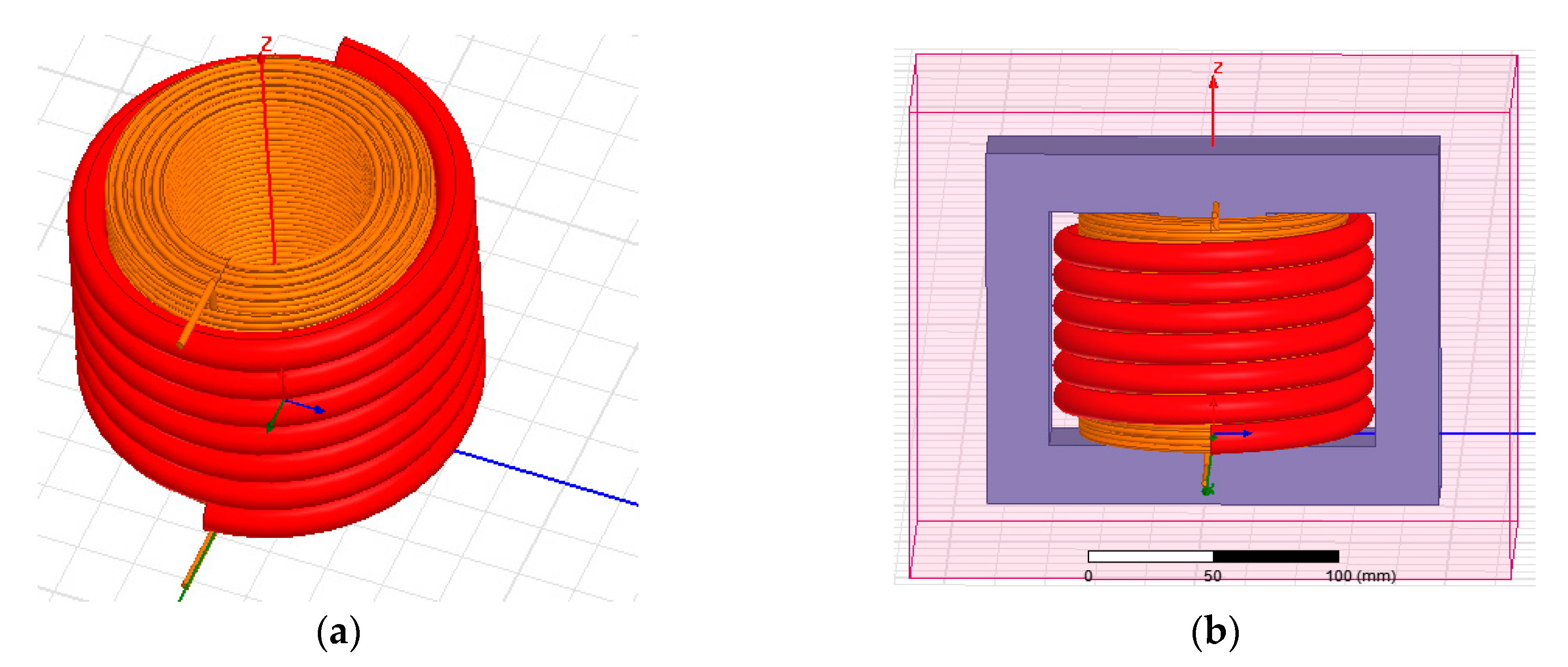
2.3. Ferrite Core High Frequency Transformer Design

The importance of ferrite materials is worth mentioning in modern power and industrial electronics application. Design constraints of ferrite materials and losses incorporated in soft magnetic materials due to high switching frequency are already discussed in literature [38,39]. More elaborate models that discuss the modeling and dependence of ferrite losses at high flux densities and high frequencies are also discussed in [40].
The operation of ferrites at square waves with 50% duty cycle offer 0%–15% smaller losses as compared to sinusoidal signals of the same peak and frequency [41,42,43,44]. These properties and performance make ferrite materials suitable for many switching applications where square wave switching is desired without using any auxiliary filter circuits.
In this research work ferrite medium, operated at 50% duty cycle within DAB, is used not only to provide galvanic isolation but also to decrease voltage levels. The ANSYS/Maxwell platform is chosen to design the high frequency ferrite core transformer. The specified design parameters of the simulated Maxwell model, as shown in Figure 7, are tabulated in Table 4.
The parameters of a high frequency transformer, simulated using ANSYS/Maxwell software, tabulated in Table 4, were used in MATLAB/Simulink to carry out the simulation of SST.

3. Simulation Results

The SST-VSC incorporated within the inner–outer control loops and voltage droop control maintained both active and reactive power requirements while the SST-VSI fulfilled variable frequency control requirements at the consumer end. The SST-VSC connected with the 11 kV grid, maintained a DC -link V D C , m e s at 20 kV whose specifications are already given in Table 1, while the SST-VSI, specifications given in Table 2, generated variable voltage and variable frequency at the load end.
Since the proposed circuit was symmetric, so the bidirectional power flow could be achieved just by changing the gate pulses only without any amendment in the circuit. To assess the flexibility and validity of the proposed circuit, simulations using the MATLAB/Simulink environment were carried out for four different test cases: SST to deliver active power, SST as a variable frequency drive, bidirectional power flow interfacing RES and SST as a power factor improvement (PFI) device.

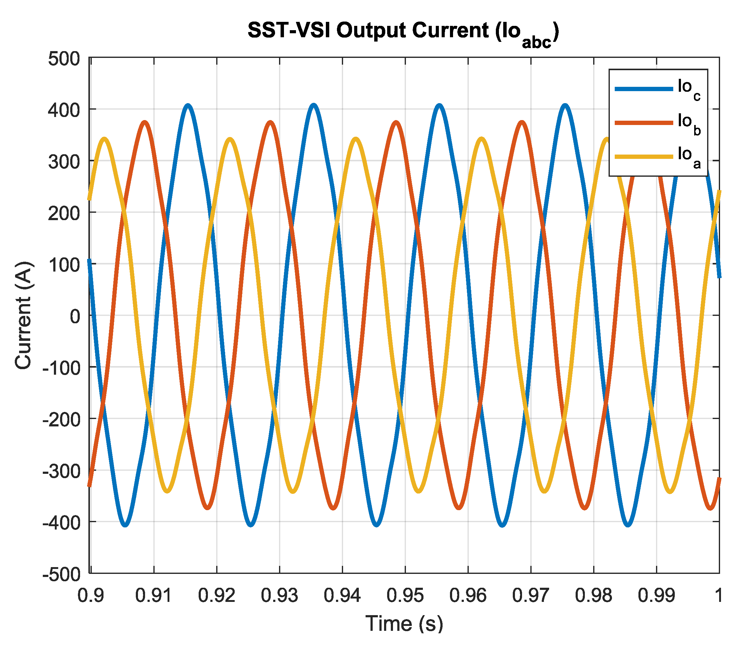
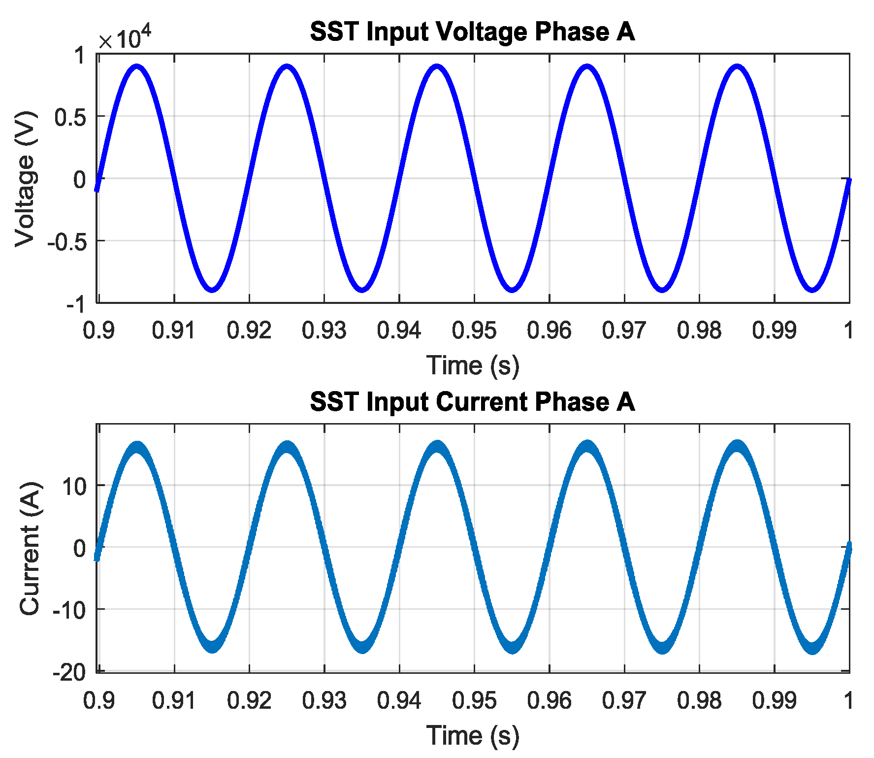
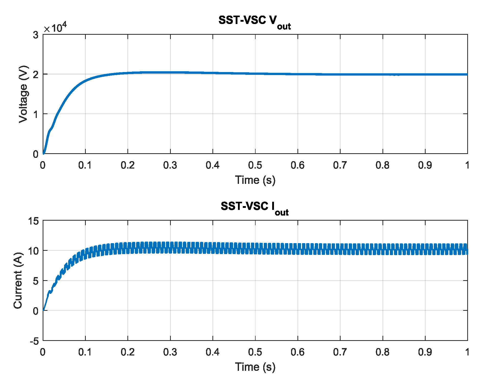
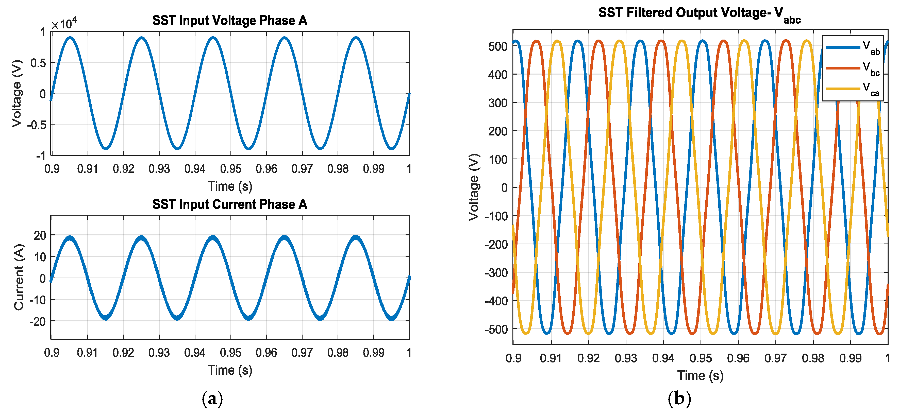
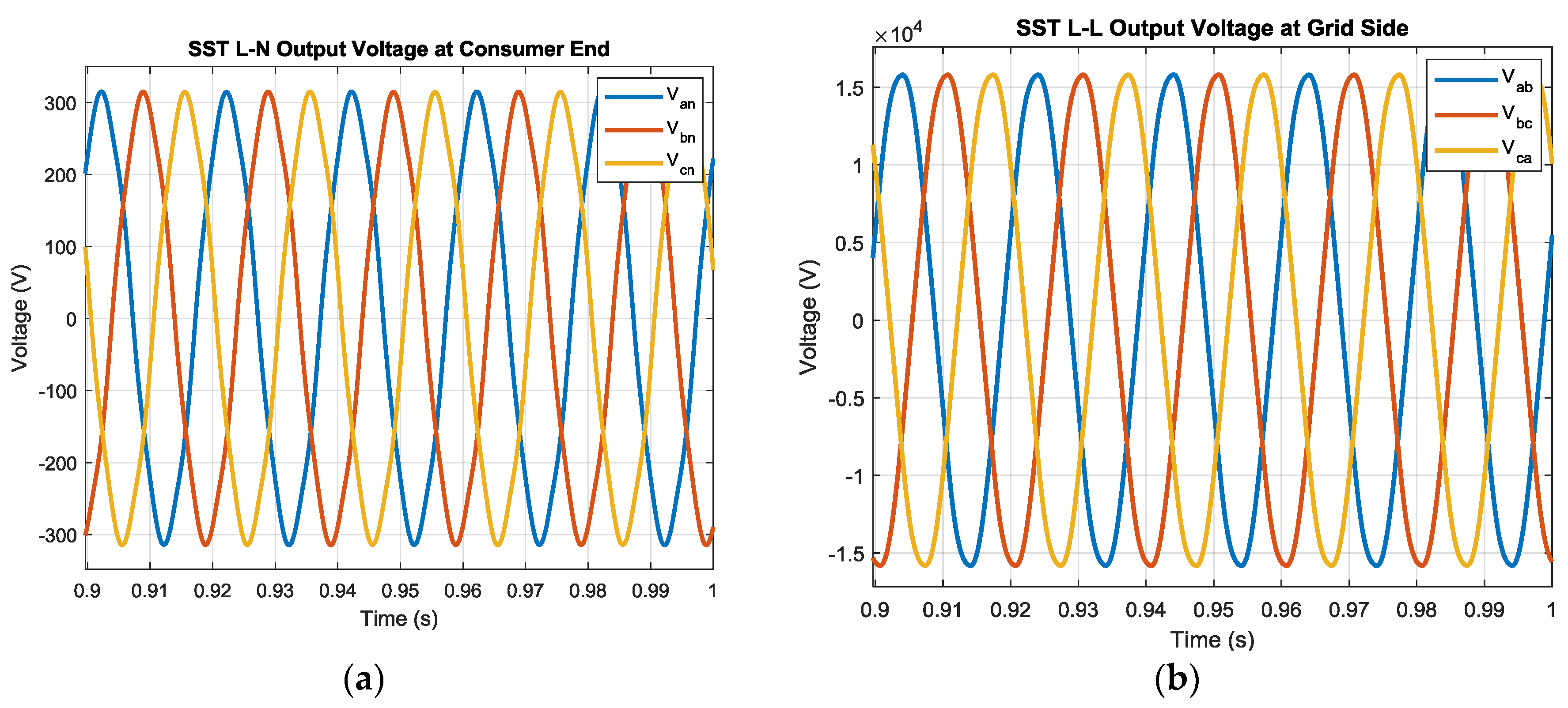
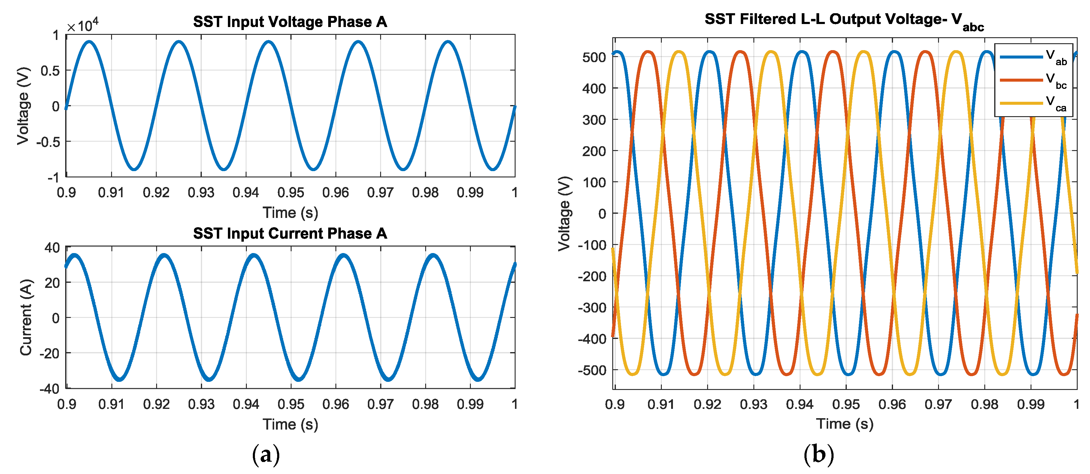
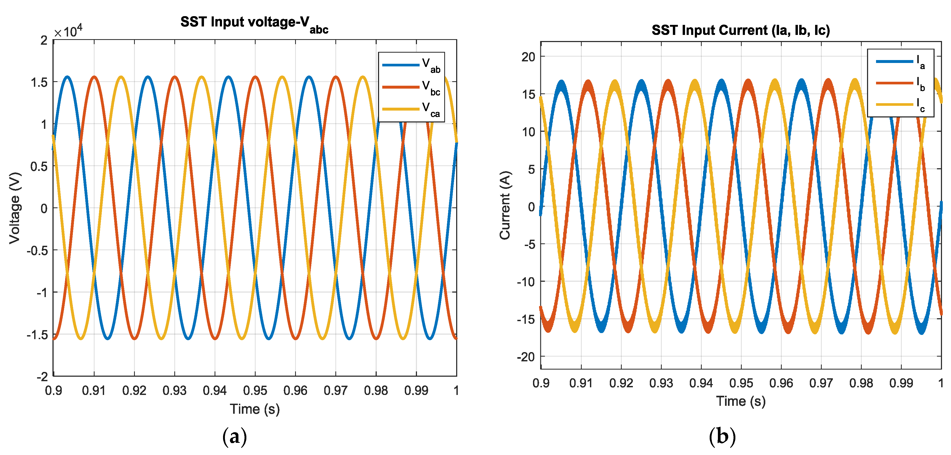
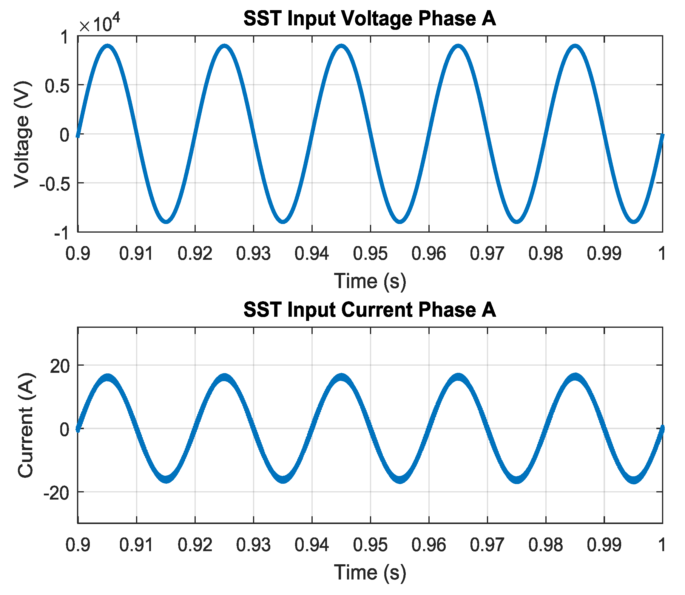
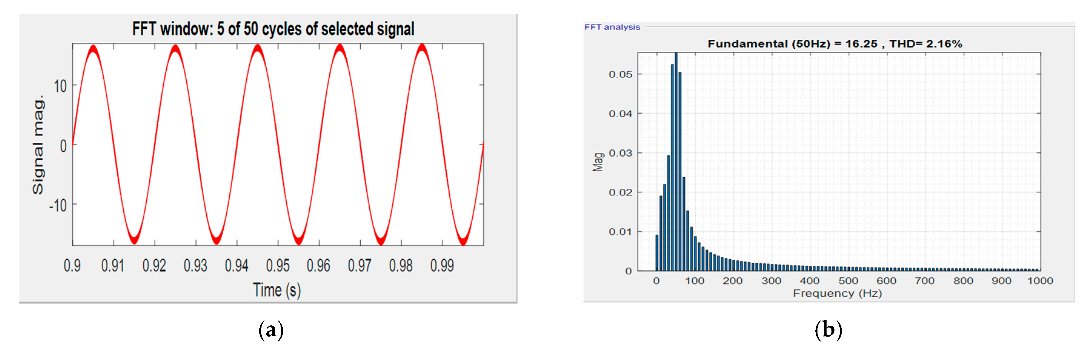
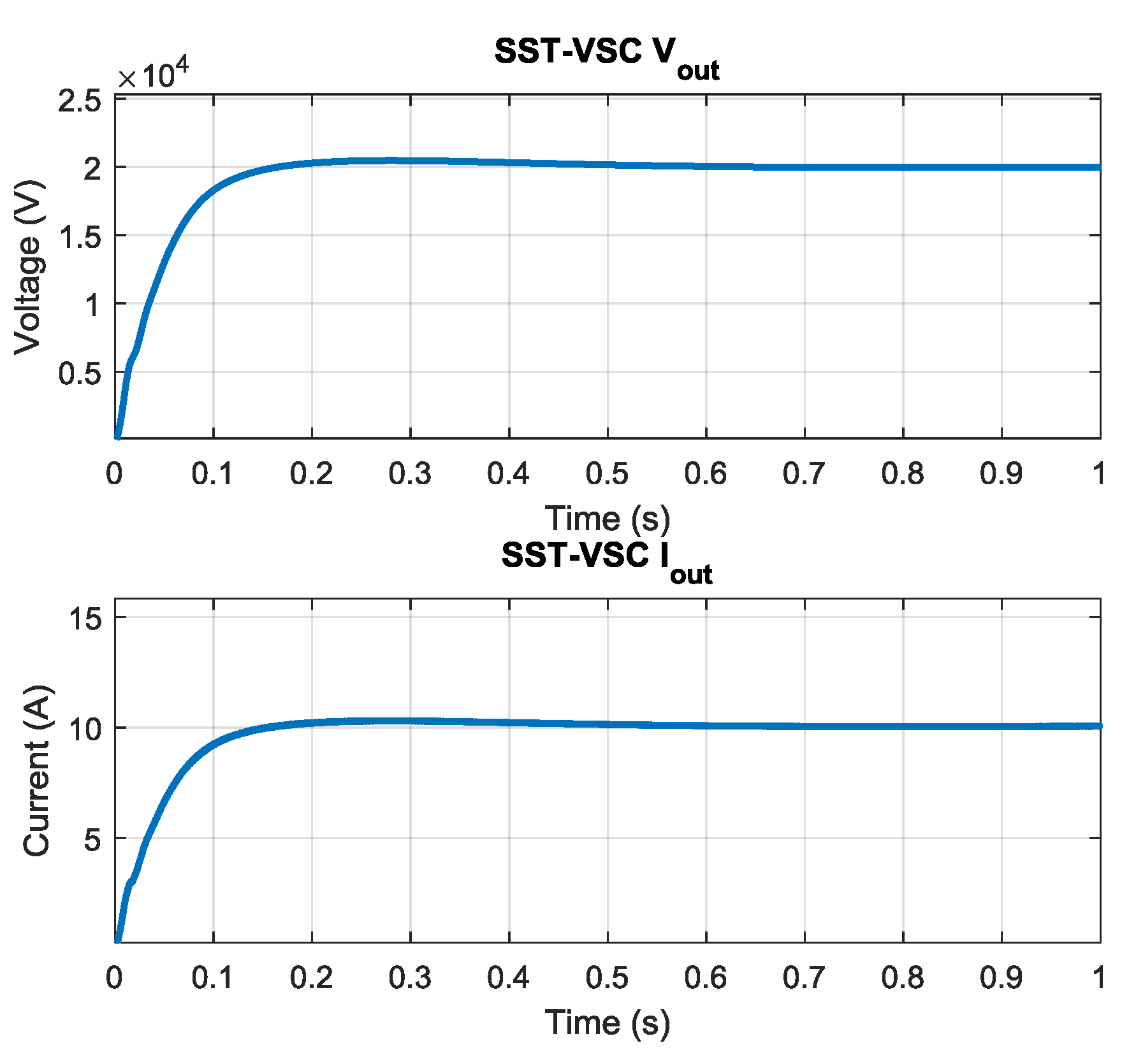
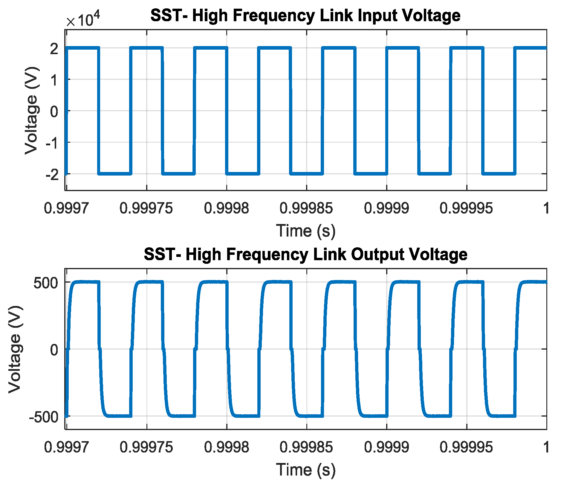
3.1. Case 1: Active Power Flow

Simulation results were presented at various stages of the proposed SST based on multi-stage power switching converters after the transient period was elapsed. Three phase voltage and current at the grid side, for a three-phase balanced load, are shown in Figure 8. As can be observed from Figure 9, SST input voltage (phase A) and current (phase A) at the grid side remained in-phase even though active power demand was varied from 0.0 p.u. to 1.0 p.u, thus delivering power at unity power factor. Results show that presented SST model drew balanced three phase current from the grid. Input current (phase A) had very less harmonic content (THD = 2.16%) as shown in Figure 10. Same results were valid for other phases as well.
In the dual active bridge (DAB) circuit, the full bridge square wave inverter cascaded at SST-VSC generated a square wave voltage of 25 kHz for the high frequency transformer (HFT), which reduced the voltage level. The other full bridge square wave converter used within DAB, rectified the voltage at the secondary side of HFT. The voltage and current response of the SST-VSC at the DC -link V D C , m e s side is given in Figure 11. Voltage at the primary and secondary side of HFT are shown in Figure 12.
At the DAB end, the DC -capacitor decreased the ripple content while the SST-VSI cascaded used SVPWM pulses to generate a three phase voltage with variable frequency and amplitude for the consumer end. When the generated frequency was 50 Hz, the SST-VSI output Line to Neutral (L-N) voltage before and after filter circuits are shown in Figure 13.
The same was true for the case of a 1.0 p.u. three-phase unbalanced load. Figure 14 and Figure 15 display that SST delivers unbalanced current to the unbalanced load while keeping the SST input voltage (phase A) and current (phase A) in-phase at the grid side, thus ensuring power at the unity power factor.
In addition, for unbalanced loaded SST, results presented in Figure 16 show that presented SST model drew a balanced three phase current from the grid with a harmonic content of 2.15% only for each phase current.
The voltage and current response of SST-VSC at DC -link V D C , m e s with unbalanced loading is given in Figure 17.

3.2. Case 2: SST as a Variable Frequency Drive

When the operation of SST as VFD was evaluated for the case when SST delivered power to an induction motor with 1.0 p.u mechanical loading, the obtained results showed satisfactory results. SST maintained the unity power factor. The grid side current harmonic contents were within IEEE defined THD limits. With the induction motor at the rated loading, the settling time of SST-VSC at the DC -link increased by 0.15 s, as shown in Figure 18. SST-VSC took a little bit more (0.32 s) time to settle for the inductive load.
For the case when SST generated the voltage signal of 50 Hz for the inductive load, it could be observed from Figure 19 that the SST input current and the voltage were in phase, thus ensuring the unity power factor. For this case, filtered SST output voltage is shown in Figure 20.
When SST generated 60 Hz voltage signal for the load, the same parameters were evaluated, as in the previous case, and are displayed in Figure 21. Similarly, a voltage signal of other frequencies can be generated using the proposed SST for the resistive as well as the inductive load.

3.3. Case 3: SST with a Renewable Interface

To cope with the increasing trend of using RESs, SST provides a very handy infrastructure. RES integrated with SST, as shown in Figure 1, can be used solely to provide power to the consumer, making SST working as stand-alone system. The proposed topology also makes bidirectional power flow possible just by changing the gate pulses of the SST-VSC to make it perform as SST-VSI.
A high frequency transformer, which in previous cases was used to reduce the voltage level, now in this scenario, was working as a step up HFT. DAB, in this case, would maintain the DC -link for the SST-VSC. The SST-VSC, now working as SST-VSI, used SVPWM pulses to generate a three phase voltage. In this scenario SST was working as a grid-tied inverter, feeding power to the utility.
The RES block, represented in Figure 1, would be any single RES or the hybrid-RES incorporating batteries as well. In this research work, only the design of controlled multi-input multi-output circuitry of SST is under investigation, so, no specific constraints regarding the RESs were taken into consideration.
When a constant DC source was used as RES, simulations show that SST provided power not only to consumer but also to the utility as well, as shown in Figure 22, so, this architecture provided by SST would be a solution to all problems that will be faced in the future when smart and super grids will be kicked in the power system.

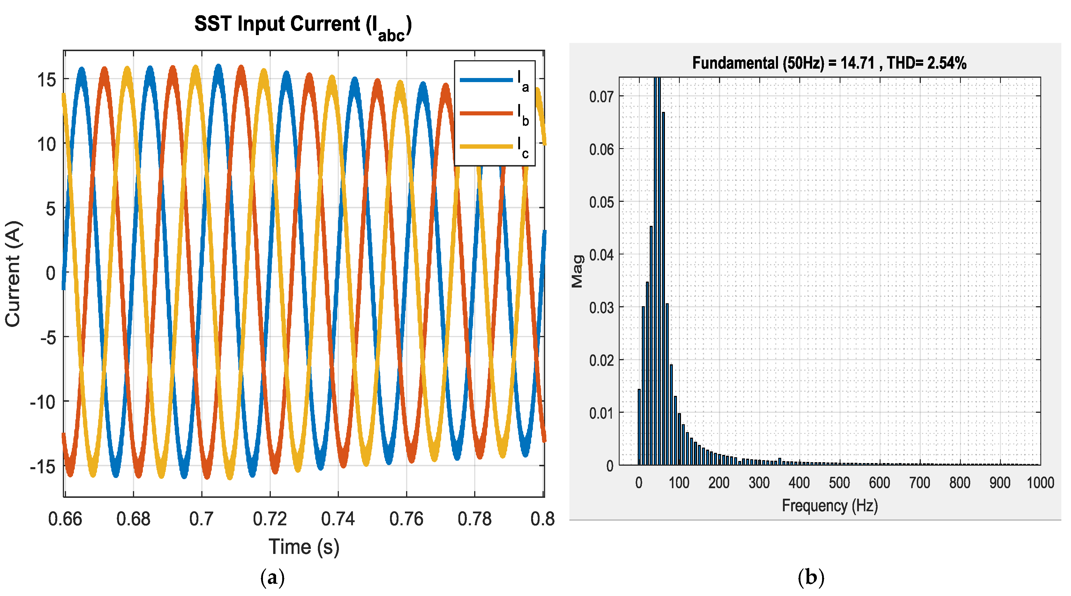
3.4. Case 4: SST as a Power Factor Improvement Device

In the ICC of SST-VSC, the quadrature component of current was maintained at zero using PI regulation, which forced SST not to draw reactive power from the grid, thus maintaining unity power factor at the grid side. When the q-component of current in ICC was maintained at any positive value, SST drew leading VAR from the grid, making SST as a PFI device, and at the same time maintaining its own feature of transformer.
When the current at the grid side was set to 45° leading, the simulation result shows that SST maintained its function of the PFI device when it was delivering power to a 1 p.u. rated inductive load. As compared to the conventional transformers, this is a remarkable achievement of the proposed SST design. The proposed circuit as a part of the interconnected system had the ability to improve the overall power factor of the system while meeting the lagging reactive power requirement of the load. However, the current at the grid side increased as expected. Figure 23 shows the voltage and current of phase A at the grid side, and filtered output voltage of the SST.
When SST as a PFI device was investigated by the pre-tuned PI controller parameters, simulation results show that SST-VSC took more time (0.7 s) to settle its steady state value (see Figure 24). The voltage droop control at the outer layer of the SST-VSC could be re-tuned to reduce the settling time of the SST-VSC.

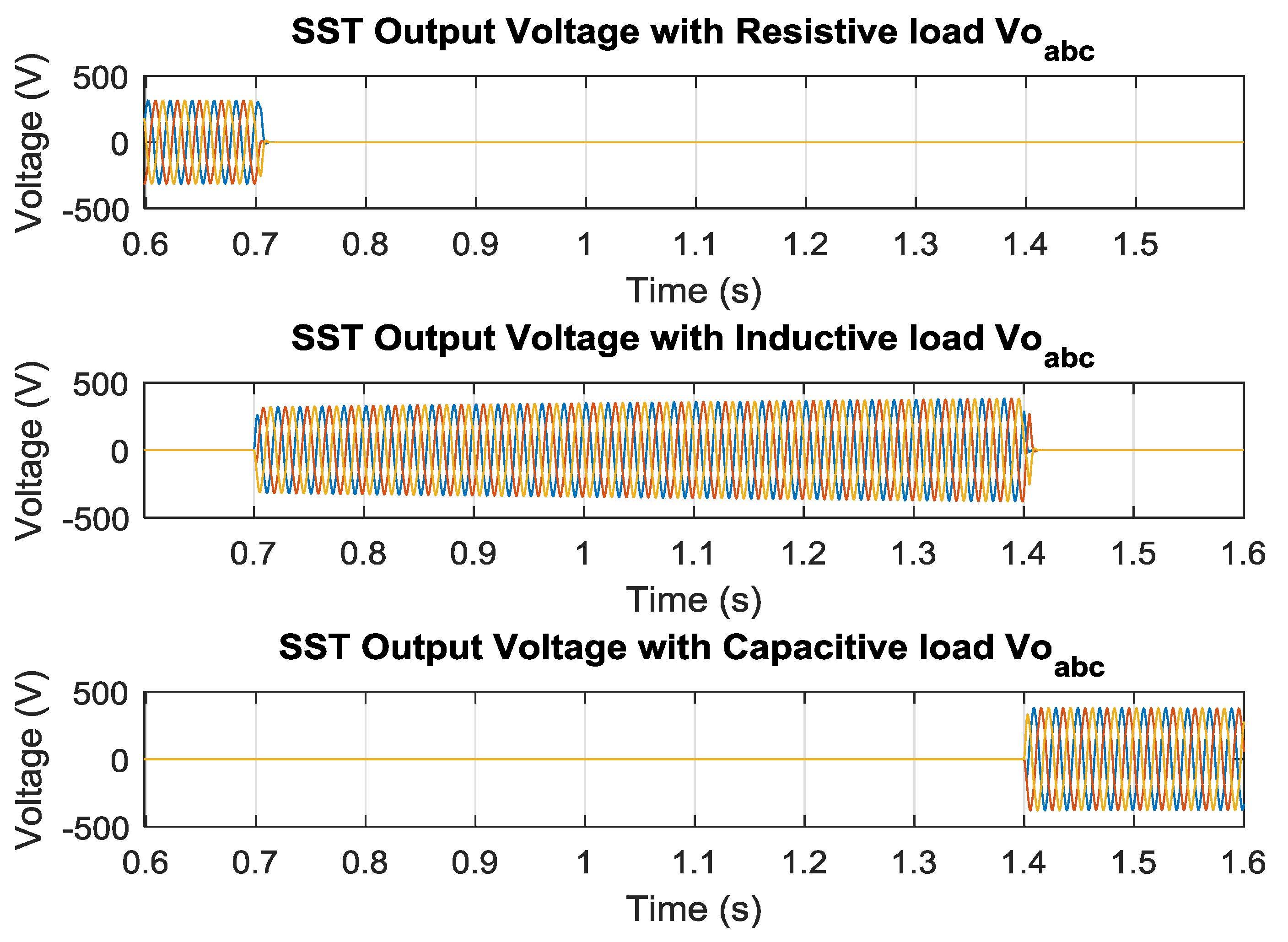
3.5. Case 5: SST Supplying Power to Instantly Shifted Different Loads

In order to verify the stable performance of the proposed SST, simulation results were presented at various stages for different shifts of loads. The simulation was performed for 1.0 p.u three different test loads, which were resistive, inductive and capacitive in nature. Just like case 1, when the system was energized, it provided only the active power to the load. The test scenario was created such that at 0.7 s, the resistive load was disconnected and the pure inductive load was connected instantly. As simulation goes on, at 0.14 s, the pure inductive load was disconnected and the pure capacitive load was connected instantly. These shifts of loads where SST instantly shifted to provide lagging VARs and leading VARs to the load are depicted in Figure 25.
When SST was energized with the resistive loading, this scenario was analogous to Case 1. When the resistive load was disconnected and the pure inductive load was connected at 0.7 s, the output current of the inverter to the load is displayed in Figure 26. At 0.7 s from Figure 26, a shift of 90 degrees in the output current can be seen clearly.
As the load shifted at 0.7 s, output current increased for a cycle to fulfill the instant lagging reactive power demand of the load and then settled down. During and after this transition time, the SST input voltage (phase A) and current (phase A) at the grid side remained in phase, as shown in Figure 27, thus supplying power at the unity power factor just like the previous scenario. The three phase supply current to the SST at the grid side was still balanced and harmonic content was still low. These results are depicted in Figure 28.
Figure 29 shows the output current of the SST at the instant when the pure inductive load was disconnected at 1.4 s, and pure capacitive load was connected instantly. Again from Figure 29, the phase shift in the output current could be visualized easily. As the load was instantly shifted to capacitive nature, the instant leading reactive power demand caused the output current of the SST to be increased at 1.4 s. The current settled down when the transient period of one cycle elapsed.
During and after the instant when SST shifted from delivering lagging VARs to the leading VARs, SST maintained its feature of operating at the unity power factor. Only for phase A, in-phase SST input voltage and input current are shown in Figure 30 while the same results were valid for the other phases as well.
SST still maintained the balanced three phase current at the grid side with only 1.89% THD. These results are shown in Figure 31.
When the load shifted to capacitive nature, the output current of the SST increased at 1.4 s as shown in Figure 29. Figure 31 displays yet another interesting result. Input current to the SST from the grid side also increased at 1.4 s, but the THD of the balanced input current was further decreased.

4. Conclusions

To replace conventional bulky transformers, a reduced-size ‘isolated’ SST was proposed in this research. Either the source was single phase, three phase or DC source. The proposed SST model could generate the single phase, three phase or DC voltage for any type of resistive or inductive load. When interfaced with RES, the symmetric configuration of SST made it working as a stand-alone system at the consumer end as well as the grid-tied inverter at the grid side. Simulation results were assessed for scenarios where SST acted as a variable frequency drive and as a power factor improvement device. In addition, when interfaced with RES, SST ensured bidirectional power flow as well. Simulation results validated the performance of the proposed SST for all the scenarios. Working of SST as the VFD and PFI device with a renewable interface makes it ideal for industrial applications where the proposed SST topology may eliminate the requirements of bulky conventional transformer especially for motor drive applications. This justifies the role of SST as VFD. The four-quadrant operation of controlled switches with the DC port within SST enables it to be integrated with the micro/super grids. The proposed SST design has the ability to reject grid side disturbances, and regulate VAR at the grid side and voltage levels for the consumer end. The presented topology of SST can easily support the wide range operation of the distribution system. Future work would be development of the hardware setup for the proposed SST topology, thus to check the validity of the proposed SST model on real time industrial applications. Apart from SST design, optimized integration of SST with hybrid-RES would be a design worth of importance.

Author Contributions

U.T., G.A., D.O.G., U.F., A.R. and M.U.A. suggested the idea, performed the simulations and managed the paper. V.E.B, M.M.B. and J.G. assisted in the idea development and paper writing.

Funding

This research received no external funding.

Conflicts of Interest

The authors declare no conflict of interest.

Abbreviations

The following abbreviations are used in this research article:
SSTSolid State Transformer
RESsRenewable Energy Resources
THDTotal Harmonic Distortion
PIProportional Integral
PWMPulse Width Modulation
SVPWMSpace Vector Pulse Width Modulation
VSCVoltage Source Converter
VSIVoltage Source Inverter
HVDCHigh Voltage Direct Current
FACTFlexible Alternating Current Transmission
SVCStatic VAR Compensator
STATCOMStatic Synchronous Compensators
UPFCUnified Power Flow Controllers
IGBTInsulated Gate Bipolar Junction Transistor
VFDVariable Frequency Drive
DABDual Active Bridge
VOCVector (oriented) Current Control
OCCOuter Current Control
ICCInner Current Control
MIMOMulti-Input Multi-Output
PCCPoint of Common Coupling
PLLPhase Locked Loop
IMCInternal Model Control
PFIPower Factor Improvement
HFTHigh Frequency Transformer
VARVolt Ampere Reactive
Notations
The following notations are used in this research article:
V x DC voltage at DAB end/input of SST-VSI
V D C , m e s DC voltage at SST-VSC end/input of DAB
V o u t output voltage of the SST
f o u t output frequency of the SST
p c point of common coupling
v S voltage source at converter side
P m e s measured active power
P r e f reference of active power
Q m e s measured reactive power
Q r e f reference of reactive power
V A C , m e s measured AC voltage
V A C , r e f reference of AC voltage
i S current from grid to the SST
i d direct component of current
i q quadrature component of current
i d , r e f reference for d-axis component of current
i q , r e f reference for q-axis component of current
e c grid voltage
e d d-axis component of grid voltage
e q q-axis component of grid voltage
V d , r e f d-axis component of reference voltage from inner current loop
V q , r e f q-axis component of reference voltage from inner current loop
V a b c , r e f three phase voltage reference signals
k p proportional gain of PI controller
k i integral gain of PI controller
α I C C bandwidth of the current controlled system
mmodulation index
f s switching frequency
T 1 , T 2 , T Z dwell time of space vector signals in SVPWM
T S total time space vector signals in each sub cycle of SVPWM
p.u.per unit

References

  1. Lai, J.S.; Maitra, A.; Mansoor, A.; Goodman, F. Multilevel intelligent universal transformer for medium voltage applications. In Proceedings of the IEEE Industry Applications Conference, Kowloon, Hong Kong, 2–6 October 2005; pp. 1893–1899. [Google Scholar]
  2. Ronan, E.R.; Sudhoff, S.D.; Glover, S.F.; Galloway, D.L. A power electronic-based distribution transformer. IEEE Trans. Power Deliv. 2002, 17, 537–543. [Google Scholar] [CrossRef]
  3. Tahir, U.; Ali, S.A.; Azeem, O.; Khan, O.; Muzzammel, R. THD improvement of phase voltages via injection of voltage in neutral conductor for three phase four wire distribution system. In Proceedings of the 2018 International Conference on Computing, Mathematics and Engineering Technologies (iCoMET), Sukkur, Pakistan, 3–4 March 2018; pp. 1–5. [Google Scholar]
  4. Hingorani, N.G. Understanding FACTs: Concept and Technology of Flexible AC Transmission Systems; IEEE Press: Piscataway, NY, USA, 2000. [Google Scholar]
  5. Chen, Z.; Guerrero, J.M.; Blaabjerg, F. A review of state of art power electronics for wind turbines. IEEE Trans. Power Electron. 2009, 23, 1859–1875. [Google Scholar] [CrossRef]
  6. Carrasco, J.M.; Franquelo, L.G.; Bialasiewicz, J.T.; Galvan, E.R.; Guisado, C.P.; Prats, A.M.; Leon, J.I.; Moreno-Alfonso, N. Power Electronic Systems for the Grid integration of Renewable Energy Sources: A survey. IEEE Trans. Ind. Electron. 2006, 53, 1002–1016. [Google Scholar] [CrossRef]
  7. Bifaretti, S.; Zanchetta, P.; Watson, A.; Tarisciotti, L.; Clare, J.C. Advanced power electronic conversion and control system for Universal and Flexible Power Management. IEEE Trans. Smart Grid 2011, 2, 231–243. [Google Scholar] [CrossRef]
  8. Zhao, T.F.; Yang, L.Y.; Wang, J.; Huang, A.Q. 270kVA Solid State Transformer Based on 10kV SiC Power Devices. In Proceedings of the IEEE Electric Ship Technologies Symposium, Arlington, VA, USA, 21–23 May 2007; pp. 145–149. [Google Scholar]
  9. Wang, G.Y.; Baek, S.J.; Elliott, A.; Kadavelugu, F.; Wang, X.; She, S.; Dutta, Y.; Liu, T.F.; Zhao, W.X.; Yao, R.; et al. Design and hardware implementation of Gen-I silicon based solid state transformer. In Proceedings of the IEEE Applied Power Electronics Conference, Fort Worth, TX, USA, 6–11 March 2011; pp. 1344–1349. [Google Scholar]
  10. She, X.; Huang, A.Q.; Wang, G.Y. 3-D space modulation with voltage-balancing capability for a cascaded seven-level converter in a solid state transformer. IEEE Trans. Power Electron. 2011, 26, 3778–3789. [Google Scholar] [CrossRef]
  11. Grider, D.; Das, M.; Agarwal, A.; Palmour, J.; Leslie, S.; Ostop, J.; Raju, R.; Schutten, M.; Hefner, A. 10kV/120A SiC DMOSFET Half-bridge Power Modules for 1MVA Solid State Power substation. In Proceedings of the IEEE Electric Ship Technologies Symposium, Alexandria, VA, USA, 10–13 April 2011; pp. 131–134. [Google Scholar]
  12. Al-Hafri, A.; Ali, H.; Ghias, A.; Nasir, Q. Transformer-less based solid state transformer for intelligent power management. In Proceedings of the 2016 5th International Conference on Electronic Devices, Systems and Applications (ICEDSA), Ras Al Khaimah, UAE, 6–8 December 2016; pp. 1–4. [Google Scholar]
  13. Drabek, P.; Peroutka, Z.; Pittermann, M.; Cedl, M. New configuration of traction converter with medium-frequency transformer using matrix converters. IEEE Trans. Ind. Electron. 2011, 58, 5041–5048. [Google Scholar] [CrossRef]
  14. She, X.; Huang, A.Q.; Wang, F.; Burgos, R. Wind energy system with integrated active power transfer, reactive power compensation, and voltage conversion functions. IEEE Trans. Ind. Electron. 2013, 60, 4512–4524. [Google Scholar] [CrossRef]
  15. Falcones, S.; Mao, X.; Ayyanar, R. Topology comparison fr solid state transformer implementation. In Proceedings of the IEEE Power and Energy Society General Meeting, Providence, RI, USA, 25–29 July 2010; Volume 25–29, pp. 1–8. [Google Scholar]
  16. Basu, K.; Mohan, N. A single-stage power electronic transformer for a three-phase PWM AC/AC drive with source-based commutation of leakage energy and common-mode voltage suppression. IEEE Trans. Ind. Electron. 2014, 61, 5881–5893. [Google Scholar] [CrossRef]
  17. Madhusoodhanan, S.; Tripathi, A.; Patel, D.; Mainali, K.; Kadavelugu, A.; Hazra, S.; Bhattacharya, S.; Hatua, K. Solid state transformer and MV Grid tie applications enabled by 15 kV SiC IGBTs and 10 kV SiC MOSFETs based multilevel converters. IEEE Trans. Ind. Appl. 2015, 51, 3343–3360. [Google Scholar] [CrossRef]
  18. Wang, L.; Zhang, D.; Wang, Y.; Wu, B.; Athab, H.S. Power and voltage balance control of a novel three-phase solid-state transformer using multilevel cascaded H-bridge inverters for microgrid applications. IEEE Trans. Power Electron. 2016, 31, 3289–3301. [Google Scholar] [CrossRef]
  19. She, X.; Huang, A.Q.; Rolando, B. Review of Solid-State Transformer Technologies and Their Application in Power Distribution Systems. IEEE J. Emerg. Sel. Top. Power Electron. 2013, 1, 186–198. [Google Scholar] [CrossRef]
  20. Muzzammel, R.; Tahir, U. Maximization of Transfer Ratio and Minimization of Harmonics in Three Phase AC/AC Matrix Converter. Curr. J. Appl. Sci. Technol. 2017, 21, 1–21, ISSN 2231–0843. [Google Scholar] [CrossRef]
  21. Chen, H.; Divan, D. Design of a 10-kV·A Soft-Switching Solid-State Transformer (S4T). IEEE Trans. Power Electron. 2018, 33, 5724–5738. [Google Scholar] [CrossRef]
  22. Reddy, B.; Dheeraj, Dr. Sahoo; Kumar, S. Design of Solid State Transformer. Int. J. Adv. Res. Electr. Electron. Instrum. Eng. 2015, 4, 56–77. [Google Scholar]
  23. Wu, G. Analysis and design of vector control for VSC-HVDC connected to weak grids. CSEE J. Power Energy Syst. 2017, 3, 115–124. [Google Scholar] [CrossRef]
  24. Rouzbehi, K.; Miranian, A.; Candela, J.I.; Luna, A.; Rodriguez, P. A generalized voltage droop strategy for control of multiterminal DC grids. IEEE Trans. Ind. Appl. 2015, 51, 607–618. [Google Scholar] [CrossRef]
  25. Rouzbehi, K.; Zhang, W.; Candela, J.I.; Luna, A.; Rodriguez, P. Unified reference controller for flexible primary control and inertia sharing in multi-terminal voltage source converter-HVDC grids. IET Gener. Transm. Distrib. 2017, 11, 750–758. [Google Scholar] [CrossRef]
  26. Raza, A.; Dianguo, X.; Yuchao, L.; Xunwen, S.; Williams, B.W.; Cecati, C. Coordinated operation and control of VSC based multiterminal high voltage DC transmission systems. IEEE Trans. Sustain. Energy 2016, 7, 364–373. [Google Scholar] [CrossRef]
  27. Gaing, Z.L. A particle swarm optimization approach for optimum design of PID controller in AVR system. IEEE Trans. Energy Convers. 2004, 19, 384–391. [Google Scholar] [CrossRef]
  28. Xu, L. Modeling, Analysis and Control of Voltage-Source Converter in Microgrids and HVDC. Master’s Thesis, University South Florida, Tampa, FL, USA, November 2013. [Google Scholar]
  29. Ottersten, R. On Control of Back-to-Back Converters and Sensorless Induction Machine Drives. Ph.D. Thesis, Department of Electric Power Engineering, Chalmers University of Technology, Göthenburg, Sweden, 2003; 165p. ISBN 91-7291-296-0. [Google Scholar]
  30. Rouzbehi, K.; Miranian, A.; Luna, A.; Rodriguez, P. Optimized control of multi-terminal DC grids using particle swarm optimization. Eur. J. Power Electron. 2014, 24, 38–49. [Google Scholar] [CrossRef]
  31. Pinto, R.T.; Bauer, P.S.; Rodrigues, F.; Wiggelinkhuizen, E.J.; Pierik, J.; Ferreira, B. A novel distributed direct-voltage control strategy for grid integration of offshore wind energy systems through MTDC network. IEEE Trans. Ind. Electron. 2013, 60, 2429–2441. [Google Scholar] [CrossRef]
  32. Rodrigues, S. A Multi-Objective Optimization Framework for the Design of Offshore Wind Farms. Ph.D. Thesis, Delft University Technology, Delft, The Netherlands, 2016. [Google Scholar]
  33. Holtz, J. Pulse width modulation for electronic power conversion. Proc. IEEE 1994, 82, 1194–1214. [Google Scholar] [CrossRef]
  34. Holmes, D.G.; Lipo, T.A. Pulse Width Modulation for Power Converters: Principles and Practice; Wiley: Hoboken, NY, USA, 2003. [Google Scholar]
  35. Rodriguez, J.; Lai, J.S.; Peng, F.Z. Multilevel Inverters: A survey of topologies, controls, and applications. IEEE Trans. Ind. Electr. 2002, 49, 724–738. [Google Scholar] [CrossRef]
  36. Binojkumar, A.C.; Siva Prasad, J.S.; Narayanan, G. Experimental investigation on the effect of advanced bus-clamping pulse width modulation on motor acoustic noise. IEEE Trans. Ind. Electr. 2013, 60, 433–439. [Google Scholar] [CrossRef]
  37. Kumar, A.; Chatterjee, D. A survey on space vector pulse width modulation technique for a two-level inverter. In Proceedings of the 2017 National Power Electronics Conference (NPEC), Pune, India, 18–20 December 2017; pp. 78–83. [Google Scholar]
  38. Bertotti, G. Hysteresis in Magnetism; Academic Press: San Diego, CA, USA, 1998; pp. 225–429. [Google Scholar]
  39. Boll, R. Soft Magnetic Materials, the Vacuumschmelze Handbook; Heyden&Son Ltd.: London, UK, 1979; pp. 13–108. [Google Scholar]
  40. Sullivan, C.R. Winding loss calculation with multiple windings, arbitrary waveforms and 2-D field geometry. In Proceedings of the IEEE IAS Annual Meeting, Baltimore, ML, USA, 3–7 October 1999; pp. 2093–2099. [Google Scholar]
  41. Li, J.; Abdallah, T.; Sullivan, C. Improved calculation of core loss with non-sinusoidal waveforms. In Proceedings of the IEEE IAS 36-th Annual Meeting, Chicago, IL, USA, 30 September–4 October 2001; pp. 2203–2210. [Google Scholar]
  42. Snelling, E.C. Soft Ferrites Properties and Applications, 2nd ed.; Butterworth-Heinemann: London, UK; Butterworth, Malaysia, 1988. [Google Scholar]
  43. Bossche, A.V.; Valchev, V.C.; Georgiev, G.B. Measurement and Loss Model of Ferrites with Non-sinusoidal Waveforms. In Proceedings of the PECS’04, Aachen, Germany, 24–28 June 2004. [Google Scholar]
  44. Valchev, V.C.; Van den Bossche, A.P.; Van de Sype, D.M. Ferrite losses of cores with square wave voltage and DC bias. In Proceedings of the 31st Annual Conference of IEEE Industrial Electronics Society, 2005, IECON 2005, Raleigh, NC, USA, 6–10 November 2005; pp. 837–841. [Google Scholar]
Figure 1. Proposed circuit diagram of the solid-state transformer.
Applsci 09 03545 g001
Figure 2. The d–q control architecture of solid state transformers-voltage source converters (SST-VSC).
Applsci 09 03545 g002
Figure 3. Inner current control loop of SST-VSC.
Applsci 09 03545 g003
Figure 4. Vector representation of the SVPWM signal.
Applsci 09 03545 g004
Figure 5. Vector representation of the SVM signal in sector 1.
Applsci 09 03545 g005
Figure 6. Gating sequence for the switches.
Applsci 09 03545 g006
Figure 7. High frequency ferrite core transformer. (a) Primary and secondary coil. (b) Complete transformer model placed within an air medium.
Applsci 09 03545 g007
Figure 8. (a) SST input voltage at the grid side. (b) SST input current at the grid side.
Applsci 09 03545 g008
Figure 9. Result displaying that phase A voltage and current are in phase with each other.
Applsci 09 03545 g009
Figure 10. (a) Phase A current drawn from utility. (b) Total harmonic distortion (THD) analysis of phase A current.
Applsci 09 03545 g010
Figure 11. SST-VSC voltage and current at the DC -link.
Applsci 09 03545 g011
Figure 12. Primary and secondary voltage of the high frequency transformer.
Applsci 09 03545 g012
Figure 13. (a) SST-VSI output voltage without filter. (b) Filtered SST output voltage.
Applsci 09 03545 g013
Figure 14. SST output current to the unbalanced load.
Applsci 09 03545 g014
Figure 15. Result displaying that phase A voltage and current are in phase.
Applsci 09 03545 g015
Figure 16. (a) SST input current at the grid side. (b) THD analysis of phase A input current.
Applsci 09 03545 g016
Figure 17. SST-VSC voltage and current at the DC -link.
Applsci 09 03545 g017
Figure 18. SST-VSC response with induction motor loading.
Applsci 09 03545 g018
Figure 19. Result displaying that phase A voltage and current are in phase.
Applsci 09 03545 g019
Figure 20. SST 50 Hz filtered output voltage.
Applsci 09 03545 g020
Figure 21. SST simulation results for 60 Hz output. (a) Phase A voltage and current in phase. (b) SST 60 Hz filtered output voltage.
Applsci 09 03545 g021
Figure 22. SST simulation results when integrated with renewable energy resource. (a) SST line to neutral voltage at the consumer end. (b) SST line to line voltage at the grid end.
Applsci 09 03545 g022
Figure 23. SST simulation results as the power factor improvement (PFI) device. (a) The input current leads the input voltage. (b) SST filtered output voltage.
Applsci 09 03545 g023
Figure 24. SST-VSC response working as the PFI device with induction motor loading.
Applsci 09 03545 g024
Figure 25. Filtered SST output voltage to resistive, inductive and capacitive load.
Applsci 09 03545 g025
Figure 26. SST output current to the load. The figure is displaying the shift in phase of the current from the resistive load to inductive load at 0.7 s.
Applsci 09 03545 g026
Figure 27. Result displaying that phase A voltage and current are in phase.
Applsci 09 03545 g027
Figure 28. (a) SST input current at the grid side. (b) THD analysis of phase A input current.
Applsci 09 03545 g028
Figure 29. SST output current to the load. The figure is displaying the shift in current from the inductive load to the capacitive load at 1.4 s.
Applsci 09 03545 g029
Figure 30. Result displaying that phase A voltage and current are in phase.
Applsci 09 03545 g030
Figure 31. (a) SST input current at the grid side. (b) THD analysis of the phase A input current.
Applsci 09 03545 g031
Table 1. VSC specifications for SST.
Nominal VoltageSpecificationsImpedance
Ac grid11 kV200 kVAR = 1 Ω L = 100 mH
DC -link20 kV
DC -capacitor20 kVSingle 880 μF
Table 2. Space vectors state and the switching sequence.
VectorSector & Vector CombinationLine to Line VoltageState
VabVbcVca
V0 (000) 000Zero
V1 (100)I    V0, V1, V2, V7+Vd0−VdActive
V2 (110)II    V7, V2, V3, V00+Vd−VdActive
V3 (010)III    V0, V3, V4, V7−Vd+Vd0Active
V4 (011)IV    V7, V4, V5, V0−Vd0+VdActive
V5 (001)V    V0, V5, V6, V70−Vd+VdActive
V6 (101)VI    V7, V6, V1, V0+Vd−Vd0Active
V7 (111) 000Zero
Table 3. Voltage source inverter (VSI) specifications for SST.
QuantitySpecifications
DC-linkInput DC Voltage500 V
DC-capacitors2- DC capacitors in seriesEach 250 V & 20 mF
VoutOutput VoltageVariable
FoutOutput FrequencyVariable
Table 4. Parameters of a high frequency ferrite transformer.
UnitsQuantityValues
3F3Ferrite (MnZn), P-Type9997 (nH/T2)
BMagnetic flux density3200 Gauss (core losses <100 mW/cm3)
WaAcProduct of Core Area and Window Winding Area1006.7857 cm4
AcCore Area25 cm2
WaWindow Winding Area40.271429 cm2
PoPower200 kVA
FFrequency25 kHz
JCurrent Density3.5 A/mm2
KFilling Factor0.6
VpPrimary Voltage20 kV
IpPrimary Current (with 5% increase in input power to cover losses)10.5 A
VsSecondary Voltage500 V
IsSecondary Current400 A
NpPrimary Turns250 Turns
NsSecondary Turns7 Turns
RpPrimary Winding Resistance0.299947 Ω
LpPrimary Winding Inductance26676.98 μH
RsSecondary Winding Resistance0.34242 mΩ
LsSecondary Winding Inductance400.904 μH
ApwPrimary Winding Wire Area (with skin effect compensation)4.399 mm2
AswSecondary Winding Wire Area (with skin effect compensation)122.23 mm2

