Microstructure of Joint between Stranded Wire and Substrate Welded by Ultrasonic Welding
by
Chihiro Iwamoto
1,*, 
Keisuke Yamauchi
1,
Kazuki Motomura
2,
Yoichi Hashimoto
2 and
Kensuke Hamada
3 1
Department of Materials Science and Engineering, Ibaraki University, 4-12-1 Nakanarusawa, Hitachi, Ibaraki 316-8511, Japan
2
Dai-ichi Seiko Co., LTD., Machida ST Bldg., 1-33-10 Morino, Machida-City, Tokyo 194-0022, Japan
3
Ultrasonic Engineering Co., LTD., 1-6-1 Kashiwa-cho, Tachikawa, Tokyo 190-8522, Japan
*
Author to whom correspondence should be addressed.
Appl. Sci. 2019, 9(3), 534; https://doi.org/10.3390/app9030534
Submission received: 31 December 2018
/
Revised: 30 January 2019
/
Accepted: 1 February 2019
/
Published: 5 February 2019
(This article belongs to the Special Issue Selected Papers from the NMJ2018)
Abstract
:In order to improvement electronic and mechanical properties, welding between stranded wires and terminals is important. However, welding methods to obtain high-quality joints using stranded wires are still limited. In this report, we applied ultrasonic welding to join a Cu stranded wire to a Cu substrate. Cross-sections of the weldments were taken and observed by several microscopy techniques to elucidate the weldability and soundness of the joints. After ultrasonic welding, each wire in the stranded wire was joined together at the region where the stranded wire was joined to the substrate without any defect. Each wire was welded through the Ag coating layer, and the stranded wire and the substrate was also welded through the outermost coating layers. It was found that ultrasonic welding is an efficient technique for producing high quality joints without any defect at the interface.
1. Introduction
A coaxial connector is used to conduct high frequency signals to some devices. Recently, high quality connectors with low loss transmission have been required to achieve high capacity and high-speed communication. One of the key factors is the welding between the coaxial connector and coaxial cable. The coaxial cable consists of the outer conductors and the core stranded wires. In general, crimping is widely used to join the connector with both the outer conductors and the stranded wires. However, the mechanical strength and conductivity of the joint between the stranded wires and substrates tends to decrease at high temperature aging due to the oxidation at the interface [1,2,3]. For single Cu wire or ribbon welding, ultrasonic welding is an attractive method and has been studied by several researchers [4,5,6,7,8,9,10,11,12]. Within this method, the joint is quickly obtained without an external heat source in the air. Cu wires can be directly welded to Cu substrates [5,10,11,12]. Further, coating of Cu wires or substrates by several metal layers for ultrasonic welding was developed to improve the weldability [4,8,9,13,14,15]. To develop the welding techniques for the joint between the coaxial connector and the wire with low loss transmission of high frequency signal, we firstly applied the ultrasonic welding to the fine stranded Cu wire. In this paper, the joint between the fine stranded Cu wire with the Ag coating and a Cu substrate with Ni and Au coating layer was investigated. To make sure of the effectiveness of the welding, the microstructure of the welded interface was investigated using several electron microscopy techniques.
2. Materials and Methods
The stranded wire consisted of 7 Cu wires with a 70 μm in diameter. Each wire was coated with an Ag layer 1μm in thickness. Figure 1 shows the electron back scatter diffraction-inverse pole figure (EBSD-IPF) map of one of the stranded wires cut parallel to the wire direction. The grain size of the Cu ranged from 5 to 10 μm. The Cu substrate was 100 μm in thickness and covered by 20 μm thick Ni and 100 nm thick Au. Figure 2 shows the schematic illustration of the ultrasonic welding machine. The welding machine used in this study was a rotary head type ultrasonic wire bonder (REBO-7WL, Ultrasonic Engineering Co., LTD., Tokyo, Japan). The wedge tool had a V-groove structure. The depth and the width of the grooves were 140 μm and 220 μm, respectively. The length of the groove was 300 μm. The stranded wire was put on the substrate between the tool and an anvil. Ultrasonic vibration and load were applied to the wire through the wedge tool during the ultrasonic welding. The welding frequency was 110 kHz, and the welding time was fixed at 0.2 s. The loading force and ultrasonic power were changed from 720 to 780 gf and, 110 to 150 a.u., respectively. After the welding, a tensile shear test was carried out for each joint. In the test, the substrate was fixed, and the wire was pulled parallel to the substrate surface with a cross-head speed of 25 mm/min. The joint welded with 750 gf in loading force and 130 a.u. in ultrasonic power showed a maximum strength of 4.8 N and was used for the microstructure observation. Joints welded over 760 gf in loading force and 150 a.u. in ultrasonic power were broken at the boundary of the wire between the original part and the applied ultrasonic part due to the damage produced by the ultrasonic welding. A detailed analysis is beyond the scope of the present paper and will be conducted in future.
Figure 3a shows the scanning electron microscope (SEM) image of the joint between the coaxial cable and the substrate after ultrasonic welding. The outer cables and covering materials in the coaxial cable were removed and the stranded wire was welded to the substrate. Figure 3b shows the morphology of the joint with maximum strength after the tensile shear test. The welded region remained on the substrate and the sample was broken in the wire.
As for the microstructure observation, the joint was cut parallel and perpendicular to the wire direction. A cross-section of the joint was polished mechanically and finished by ion-milling (IM4000, Hitachi High-Technologies, Tokyo, Japan), and observed by SEM (SU-5000, Hitachi High-Technologies, Tokyo, Japan). For the transmission electron microscope (TEM) observation, a thin sample was picked up from the cross-section using a focused ion beam (FIB) technique (JIB-4600F, JEOL, Tokyo, Japan) and observed by TEM and scanning transmission electron microscope (STEM) (JEM-2010, JEM-2800, JEOL, Tokyo, Japan).
3. Results
3.1. Macroscopic Morphology of the Welded Stranded Wire
Firstly, cross-sections of the wire were cut parallel and perpendicular to the wire direction and were observed in order to investigate the macroscopic morphology of the joint.
Figure 4 shows the typical morphology of the welded stranded wire cut perpendicular to the wire direction. Figure 4 corresponds to the cross-section of the welded region in Figure 3. After the welding, the cross-section of the stranded wire was triangular, corresponding to the wedge tool geometry, which enabled us to form a wider contact region with the substrate. In the stranded wire, several regions were separated by white lines. These regions corresponded to each wire in the stranded wire. The deformation modes varied depending on the position of the wire in the stranded wire. Wires adjacent to the substrate became flatter than the wires at the top of the welded joint. As subsequently shown, the white regions appearing at the interface areas correspond to the Ag coating along the surface of the wires prior to welding. The Ag coating layer mostly remained between the wires even after welding.
Figure 5 shows the IPF map taken from a similar cross-section of the wire in Figure 4. The color variation in the map shows the different grain orientations. Arrows denote the positions of the Ag layer between the wires. The stranded wire consists of seven thin wires. However, most of the cross-section of the stranded wire looks green, suggesting that the seven wires showed the same specific orientation after ultrasonic welding.
Figure 6 shows one of the cross-sections of the welded stranded wire cut parallel to the wire direction. Along the wire direction, a 200 μm wide, large welded interface was formed between the wire and the substrate. Each wire around the welded interface was almost parallel to the interface.
3.2. Microstructure at the Interface Between the Wire and Substrate
In this section, the detailed microstructure of the interface was investigated in order to elucidate the welding mechanism.
Figure 7 shows the typical interface microstructure between the wire and the substrate. Grey and white regions which correspond to the Ag and Au are observed between the Cu and the Ni. Ag is the coating layer of the Cu wire and Au is the outermost layer on the Cu substrate. The morphology of the Ag and Au layers were rough and the thickness of each layer varied depending on location suggesting that the plastic flow between Ag and Au occurred during the ultrasonic welding. Occasionally small pores were observed at the interface between the Ag and Au indicating the original surface position. No other defects were observed at the interface.
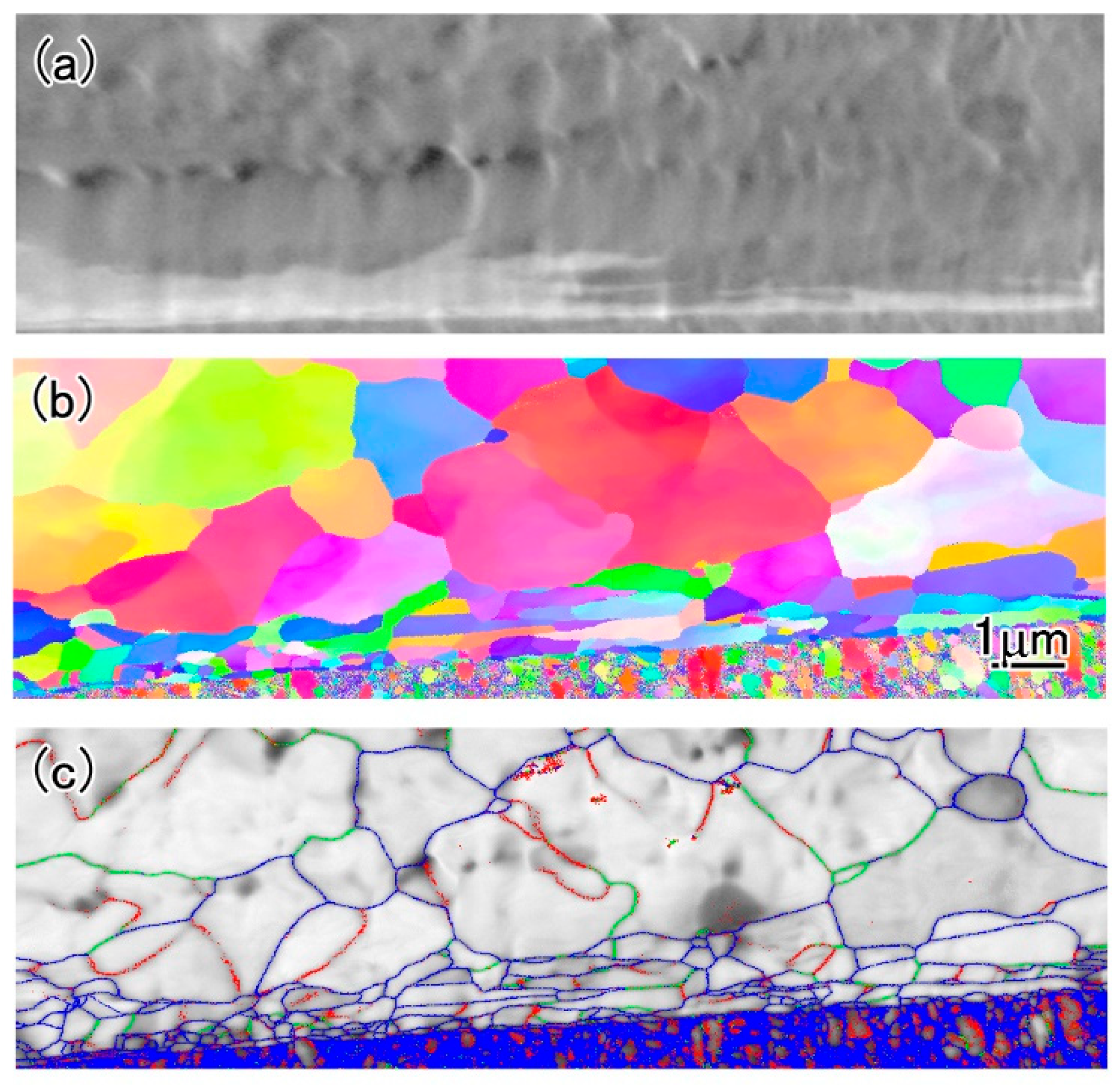
Figure 8 shows the IPF map and EBSD grain boundary map at the interface. Figure 8a shows the SEM image of the interface taken from a similar region as the EBSD analysis in Figure 7. In the IPF map in Figure 8b, elongated small Ag grains were observed in the Ag layer adjacent to the large Cu grains. Along the interface, grains extended from 1 to 2 μm. In contrast, the thickness of the grains was about 200 nm in average and perpendicular to the interface. Figure 8c shows the EBSD grain boundary map. In this map, blue lines indicate that the grain boundary misorientation is over 15°, and the grain boundary is a high angle grain boundary. Green lines indicate that the rotation angle ranges from 15° to 5°. Red lines indicate that the rotation angle is less than 5°. It was found that the Ag layer mostly consisted of high angle grain boundaries, and the Cu grains contained many small angle grain boundaries.
To confirm the composition of each layer observed between the wire and the substrate, the composition mapping was taken using EDS installed in STEM. Figure 9 shows a typical STEM image around the interface and EDS mapping taken from the same region of the STEM image. The Ni and Au layers are present on the Cu plate as the substrate. On this substrate, there is Ag which is the coating layer on the Cu wire. It was revealed that after the ultrasonic welding, these layers remained intact and the contrast difference in each layer corresponded to the composition variation.
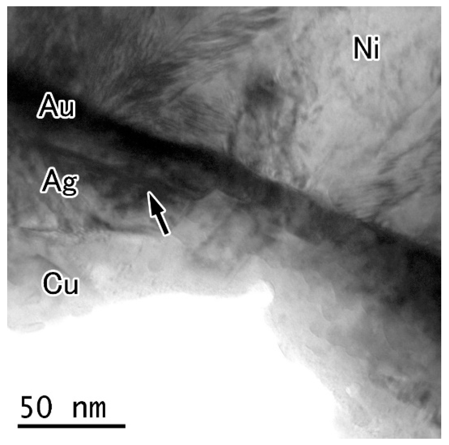
Figure 10 shows the bright field image at the welded interface between the wire and the substrate. In the Ag layer, twin boundaries were observed parallel to the interface, which was thought to be caused by the plastic deformation during the ultrasonic welding. No clear interface between the Au and Ag was observed at this region. Chemical composition mapping was taken at a similar region of the interface. Figure 11 shows the STEM image and the composition maps of the Ag grain adjacent to the welded interface. In the Ag grain, Au exists without a clear boundary, and the density of the Au increases near the substrate. An Ag/Au solid solution is present at this region.
3.3. Microstructure at the Interface Between Wires
In Figure 4, it was shown that there was a strong adhesion between wires in the stranded wire after ultrasonic welding. To confirm this, we observed the microstructure of the interface between wires in detail.
Figure 12 shows the typical enlarged image of the interface between wires in the stranded wire. The white region is the Ag coating which was present at the surface of the wire before welding. Occasionally small pores were observed along the Ag/Ag interface indicating the original surface position. It was revealed that after the ultrasonic welding, both interfaces between the substrate and the stranded wire and each wire in the stranded wire joined together simultaneously.
Figure 13 shows the IPF map and EBSD grain boundary map around the interface between the welded wires. Figure 13a shows the SEM image of the interface taken from a similar region to the EBSD analysis in Figure 12. The IPF map in Figure 13b shows that the Ag grains are elongated along the interface. In the EBSD grain boundary map in Figure 13c, the Ag layer mostly consists of high angle grain boundaries and Cu grains containing many small angle grain boundaries. The distribution of the grain boundary character was near similar to the interface between the wire and the substrate.
4. Discussion
After ultrasonic welding, the Cu wire deformed to a triangle shape as shown in Figure 4. However, the interface between the stranded wire and the substrate was almost flat at the micrometer scale as shown in Figure 7. In the literature, rough interfaces are sometimes observed between the Cu wire and substrates welded by ultrasonic welding [11,16]. The flat interface produced in the present experiment was considered to be caused by the hard Ni layer covering the Cu substrate.
The EBSD analysis in Figure 8 and Figure 13 showed that small elongated grains were present along the interface with high angle grain boundaries. Production of the fine-grained region by severe plastic deformation along the interface is frequently reported in the literature after ultrasonic welding process in several systems [16,17,18,19]. Around the interface between the Cu and Ni sheets welded by ultrasonic welding, formation of the fine Cu grains, which is softer than Ni, was observed due to the plastic deformation during the welding [20]. This fine-grained region had high angle grain boundaries and was considered to be caused by a grain subdivision mechanism [21]. In the present experiment, during the ultrasonic welding, severe plastic deformation mainly occurred in the soft Ag and Au regions, leading to the formation of elongated fine grains with high angle grain boundaries.
The plastic deformation of a softer plate inserted between harder plates promoted the plastic flow and contributed to the formation of the joint by ultrasonic welding in Mg alloys [22]. In the present system, deformation of the Ag and Au layers occurred predominantly after the ultrasonic welding. Also, Ag and Au layers would be effective to minimize the Cu grain deformation and the following grain boundary formation which degrade the electronic conductivity of the Cu [23].
At some part of the interface, a solid solution was observed between the Ag and Au. Depending on the location, the thickness of the region of the solid solution from the interface varied, but it was of the order of 10 nm. Considering the short welding time of 0.2 seconds and the diffusion rate of the elements, the thickness of the solid solution seemed to increase due to the ultrasonic welding. It has been frequently reported that the excess concentration of vacancies produced by the severe plastic deformation increases the diffusion around the interface during ultrasonic welding [24,25]. Furthermore, it has been suggested that high-density dislocations, fine grains and substructures generated by ultrasonic welding can enhance diffusion [17,26,27]. Therefore, faster diffusion at the interface and the formation of the solid solution might be a common feature of ultrasonic welding in the present system. Consequently, the softer material covering the Cu and wire substrate took most of the plastic deformation, contributing to the final morphology and properties of the joint.
5. Conclusions
Ultrasonic welding was applied to a Cu stranded wire and a Cu substrate. Both interfaces between the substrate and the stranded wire and each wire in the stranded wire were efficiently welded without any large voids or cracks observed. The Ag and Au layer remained at the most region of the welded interface. The welding was successfully achieved between the Au and Ag, which covered the Cu wire and substrate, respectively. Ultrasonic welding is an attractive method for producing high quality joints without any defect at the interface. The coating layers on the Cu could effectively contribute to the joining process of the stranded wire to the substrate.
Author Contributions
Writing draft, revision, data acquisition, analysis, supervision, C.I.; sample preparation, K.Y.; welding sample, tensile shear test, discussion, K.M. and Y.H.; discussion K.H.
Funding
This research was funded by Dai-ichi Seiko Co., LTD.
Acknowledgments
A part of this work was conducted at Advanced Characterization Nanotechnology Platform of the University of Tokyo, supported by ‘‘Nanotechnology Platform’’ of the Ministry of Education, Culture, Sports, Science and Technology (MEXT), Japan.
Conflicts of Interest
The authors declare no conflict of interest.
References
- Fujimaki, H.; Sano, K. Bonding Technology of Copper Stranded Conductors. Q. J. Jpn. Weld. Soc. 1993, 11, 277–281. [Google Scholar] [CrossRef]
- Fujimaki, H.; Takaai, T.; Sano, K. Estimation of Crimping Interface of the Stranded Copper Conductor and Brass Terminal by Residual Resistance Ratio Measurements. Q. J. Jpn. Weld. Soc. 1995, 13, 418–423. [Google Scholar] [CrossRef]
- Fujimaki, H.; Takaai, T.; Sano, K. Dynamic Action Crimp Termination in Stranded Copper Conductors and Brass Terminals. Q. J. Jpn. Weld. Soc. 1995, 13, 550–555. [Google Scholar] [CrossRef]
- Kajiwara, R.; Katoh, M.; Maruta, M. Ultrasonic Bonding Phenomena of Cu Composite Wire with Au Coating. Q. J. Jpn. Weld. Soc. 1994, 12, 142–146. [Google Scholar] [CrossRef]
- Fujimoto, K.; Manabe, T.; Nakata, S.; Fujii, A. Infuluence of bonding condition and surface state on bondability. Q. J. Jpn. Weld. Soc. 1996, 14, 168–173. [Google Scholar] [CrossRef]
- Fujimoto, K.; Masutani, Y.; Nakata, S.; Fujii, A. Influence of wire deformation behavior on bondability. Q. J. Jpn. Weld. Soc. 1996, 14, 174–178. [Google Scholar] [CrossRef]
- Tian, Y.; Wang, C.; Lum, I.; Mayer, M.; Jung, J.P.; Zhou, Y. Investigation of ultrasonic copper wire wedge bonding on Au/Ni plated Cu substrates at ambient temperature. J. Mater. Process. Technol. 2008, 208, 179–186. [Google Scholar] [CrossRef]
- Tian, Y.; Wang, C.; Zhou, Y.N. Bonding mechanism of ultrasonic wedge bonding of copper wire on Au/Ni/Cu substrate. Trans. Nonferrous Met. Soc. China 2008, 18, 132–137. [Google Scholar] [CrossRef]
- Maeda, M.; Sato, T.; Inoue, N.; Yagi, D.; Takahashi, Y. Anomalous microstructure formed at the interface between copper ribbon and tin-deposited copper plate by ultrasonic bonding. Microelectron. Reliab. 2011, 51, 130–136. [Google Scholar] [CrossRef]
- Zhong, Z.W. Overview of wire bonding using copper wire or insulated wire. Microelectron. Reliab. 2011, 51, 4–12. [Google Scholar] [CrossRef]
- Kaestle, C.; Franke, J. Comparative analysis of the process window of aluminum and copper wire bonding for power electronics applications. In Proceedings of the 2014 International Conference on Electronics Packaging (ICEP), Toyama, Japan, 23–25 April 2014; pp. 335–340. [Google Scholar]
- Gross, D.; Haag, S.; Reinold, M.; Schneider-Ramelow, M.; Lang, K.-D. Heavy copper wire-bonding on silicon chips with aluminum-passivated Cu bond-pads. Microelectron. Eng. 2016, 156, 41–45. [Google Scholar] [CrossRef]
- Dohle, R.; Petzold, M.; Klengel, R.; Schulze, H.; Rudolf, F. Room temperature wedge–wedge ultrasonic bonding using aluminum coated copper wire. Microelectron. Reliab. 2011, 51, 97–106. [Google Scholar] [CrossRef]
- Fujiwara, S.; Dauskardt, R.H. Bondability of Cu wire on Cu substrate with Sn plating by ultrasonic. Q. J. Jpn. Weld. Soc. 2010, 28, 362–368. [Google Scholar] [CrossRef]
- Uno, T. Enhancing bondability with coated copper bonding wire. Microelectron. Reliab. 2011, 51, 88–96. [Google Scholar] [CrossRef]
- Czerny, B.; Khatibi, G. Cyclic robustness of heavy wire bonds: Al, AlMg, Cu and CucorAl. Microelectron. Reliab. 2018, 88–90, 745–751. [Google Scholar] [CrossRef]
- Fujii, H.T.; Endo, H.; Sato, Y.S.; Kokawa, H. Interfacial microstructure evolution and weld formation during ultrasonic welding of Al alloy to Cu. Mater. Charact. 2018, 139, 233–240. [Google Scholar] [CrossRef]
- Broll, M.S.; Geissler, U.; Höfer, J.; Schmitz, S.; Wittler, O.; Lang, K.D. Microstructural evolution of ultrasonic-bonded aluminum wires. Microelectron. Reliab. 2015, 55, 961–968. [Google Scholar] [CrossRef]
- Khatibi, G.; Weiss, B.; Bernardi, J.; Schwarz, S. Microstructural Investigation of Interfacial Features in Al Wire Bonds. J. Electron. Mater. 2012, 41, 3436–3446. [Google Scholar] [CrossRef]
- Tanaka, Y.; Fujiwara, S.; Ogura, T.; Sano, T.; Hirose, A. Ultrasonic bonding of Cu/Ni and its thermal reliability. Q. J. Jpn. Weld. Soc. 2013, 31, 66–74. [Google Scholar] [CrossRef]
- Hughes, D.A.; Hansen, N. High Angle Boundaries Formed by Grain Subdivision Mechanisms. Acta Mater. 1997, 45, 3871–3886. [Google Scholar] [CrossRef]
- Hoshi, Y.; Iwamoto, C.; Higashi, Y. Relationship between anisotropy of extruded Mg-Zn-Y alloy and ultrasonic spot weldability. Q. J. Jpn. Weld. Soc. 2018, 36, 185–192. [Google Scholar] [CrossRef]
- Onuki, J.; Tamahashi, K.; Isshiki, M. Current Status and Future Prospect of Cu Interconnects for Very High Speed LSIs. Mater. Jpn. 2011, 50, 480–487. [Google Scholar] [CrossRef] [Green Version]
- Gunduz, I.; Ando, T.; Shattuck, E.; Wong, P.; Doumanidis, C. Enhanced diffusion and phase transformations during ultrasonic welding of zinc and aluminum. Scr. Mater. 2005, 52, 939–943. [Google Scholar] [CrossRef]
- Geissler, U.; Funck, J.; Schneider-Ramelow, M.; Engelmann, H.-J.; Rooch, I.; Müller, W.H.; Reichl, H. Interface Formation in the US-Wedge/Wedge-Bond Process of AlSi1/CuNiAu Contacts. J. Electron. Mater. 2010, 40, 239–246. [Google Scholar] [CrossRef]
- Panteli, A.; Robson, J.D.; Brough, I.; Prangnell, P.B. The effect of high strain rate deformation on intermetallic reaction during ultrasonic welding aluminium to magnesium. Mater. Sci. Eng. A 2012, 556, 31–42. [Google Scholar] [CrossRef]
- Haddadi, F. Rapid intermetallic growth under high strain rate deformation during high power ultrasonic spot welding of aluminium to steel. Mater. Des. 2015, 66, 459–472. [Google Scholar] [CrossRef]
Figure 1.
EBSD map of one of the stranded wires cut parallel to the wire direction.

Figure 2.
Schematic illustration of the ultrasonic welding machine.

Figure 3.
(a) Joint between the coaxial cable and the substrate. (b) Joint broken after tensile shear test.
Figure 3.
(a) Joint between the coaxial cable and the substrate. (b) Joint broken after tensile shear test.

Figure 4.
Cross-section of the welded wire cut perpendicular to the wire direction.

Figure 5.
Inverse pole figure (IPF) map taken from the cross-section of the wire cut perpendicular to the wire direction.
Figure 5.
Inverse pole figure (IPF) map taken from the cross-section of the wire cut perpendicular to the wire direction.

Figure 6.
Cross-section of the welded wire cut parallel to the wire direction.

Figure 7.
Enlarged SEM image of the interface. The arrow denotes a small pore at the interface.

Figure 8.
(a) SEM image at the interface between the wire and the substrate (b) IPF map and (c) EBSD grain boundary map taken at the interface.
Figure 8.
(a) SEM image at the interface between the wire and the substrate (b) IPF map and (c) EBSD grain boundary map taken at the interface.

Figure 9.
STEM image and EDS mapping of each element around the interface.

Figure 10.
Bright field image of the interface. The arrow indicates a twin boundary.

Figure 11.
EDS mapping of the Ag grain around the interface.

Figure 12.
Enlarged image of the interface between wires. The arrow indicates a small pore at the interface.
Figure 12.
Enlarged image of the interface between wires. The arrow indicates a small pore at the interface.

Figure 13.
(a) SEM image around the interface between wires. (b) IPF map and (c) EBSD grain boundary map taken at the interface.
Figure 13.
(a) SEM image around the interface between wires. (b) IPF map and (c) EBSD grain boundary map taken at the interface.

© 2019 by the authors. Licensee MDPI, Basel, Switzerland. This article is an open access article distributed under the terms and conditions of the Creative Commons Attribution (CC BY) license (http://creativecommons.org/licenses/by/4.0/).
Share and Cite
MDPI and ACS Style
Iwamoto, C.; Yamauchi, K.; Motomura, K.; Hashimoto, Y.; Hamada, K. Microstructure of Joint between Stranded Wire and Substrate Welded by Ultrasonic Welding. Appl. Sci. 2019, 9, 534. https://doi.org/10.3390/app9030534
AMA Style
Iwamoto C, Yamauchi K, Motomura K, Hashimoto Y, Hamada K. Microstructure of Joint between Stranded Wire and Substrate Welded by Ultrasonic Welding. Applied Sciences. 2019; 9(3):534. https://doi.org/10.3390/app9030534
Chicago/Turabian StyleIwamoto, Chihiro, Keisuke Yamauchi, Kazuki Motomura, Yoichi Hashimoto, and Kensuke Hamada. 2019. "Microstructure of Joint between Stranded Wire and Substrate Welded by Ultrasonic Welding" Applied Sciences 9, no. 3: 534. https://doi.org/10.3390/app9030534
Note that from the first issue of 2016, this journal uses article numbers instead of page numbers. See further details here.