High-Speed Photodetectors for Microwave Photonics


ECE Department, University of Virginia, 315 McCormick Rd., Charlottesville, VA 22904, USA
*
Author to whom correspondence should be addressed.
Appl. Sci. 2019, 9(4), 623; https://doi.org/10.3390/app9040623
Submission received: 26 December 2018
/
Revised: 7 February 2019
/
Accepted: 10 February 2019
/
Published: 13 February 2019
(This article belongs to the Special Issue Microwave Photonics 2018)
Abstract
:This paper reviews high-power photodiodes, waveguide photodetectors, and integrated photodiode-antenna emitters with bandwidths up to 150 GHz. Results from heterogeneous III-V photodiodes on silicon and Ge-on-Si photodiode arrays for analog applications are presented.
1. Introduction
High-speed high-power photodiodes are critical components in microwave photonics applications including radio-over-fiber, low-phase-noise microwave signal generation, antenna remoting, and arbitrary waveform generation [1,2,3,4]. These applications require high power handling capability and high linearity of the photodiode (PD) to maintain high radio frequency (RF) gain and large spurious-free dynamic range (SFDR), respectively [5]. To achieve large RF output power at microwave frequencies, several PD structures have been reported, among which the uni-traveling carrier (UTC) PD [6,7,8] has demonstrated large bandwidth and a high saturation current. In an UTC PD, photons excite electron-hole pairs in an un-depleted absorption layer. Since only electrons are injected into the transparent drift layer, the transit time is shorter and space charge screening is reduced, compared to a conventional p-i-n PD, which has both electrons and holes in the drift region. Over the past few years, the University of Virginia (UVA) has developed InGaAs/InGaAsP/InP modified uni-traveling carrier (MUTC) PDs that achieved a high bandwidth >105 GHz, high responsivity, and low dark current [9]. Similar to UTC photodiodes, MUTC photodiodes include an InGaAs un-depleted absorber and a depleted InP drift layer. By adding a depleted InGaAs absorber with an appropriate thickness between the un-depleted absorber and the drift layer, the responsivity can further increase. This layer also maintains a high electric field and thus facilitates electron transport at the heterojunction interface. To increase RF output power and avoid saturation, the drift layer is lightly n-type doped for charge compensation. The charge from the ionized donors pre-distorts the electric field and can counteract the space charge screening effect at a high current [10]. A critical factor that limits the RF output power is Joule heating in the junction. Previously, it had been shown that significantly higher RF output power could be achieved by flip-chip bonding the PD onto a substrate with high-thermal-conductivity such as AlN or diamond [11].
2. High-Power High-Speed Photodiodes
Previously, we demonstrated back-illuminated charge-compensated MUTC PDs with 7.8 and 9.6 dBm RF output power at 110 and 100 GHz, respectively [12]. These devices included a high-impedance 200 μm-long coplanar waveguide (CPW) between the RF pads and the PD that provided inductive peaking at 100 GHz. Recently, we flip-chip bonded similar MUTC PDs to a low-inductance transmission line (TL) on a AlN submount to increase the RF output power beyond the 3 dB bandwidth. Using thermo-compression Au-Au bonding, the PD’s bonding pads were attached to a CPW with a 130-µm signal-to-ground gap. A short tapered TL connected the stub to a 50 Ω, 50 × 154-µm2 pad with a 54-µm signal-to-ground gap and 250-µm pitch (Figure 1a). This optimized CPW design decreased the roll-off of the frequency response beyond 100 GHz and extended the usable frequency range up to 160 GHz. Figure 1b shows the measured RF output power and compression at 160 GHz using an optical heterodyne setup, a GGB Industries WR-6 waveguide probe with bias-T, and a VDI power meter PM5. A 9-µm diameter PD reached a maximum RF output power of −2.6 dBm at 160 GHz and −3 V, and a saturation current of 40 mA. The dark current was 0.4 nA and the responsivity was 0.2 A/W at 1550 nm [13].
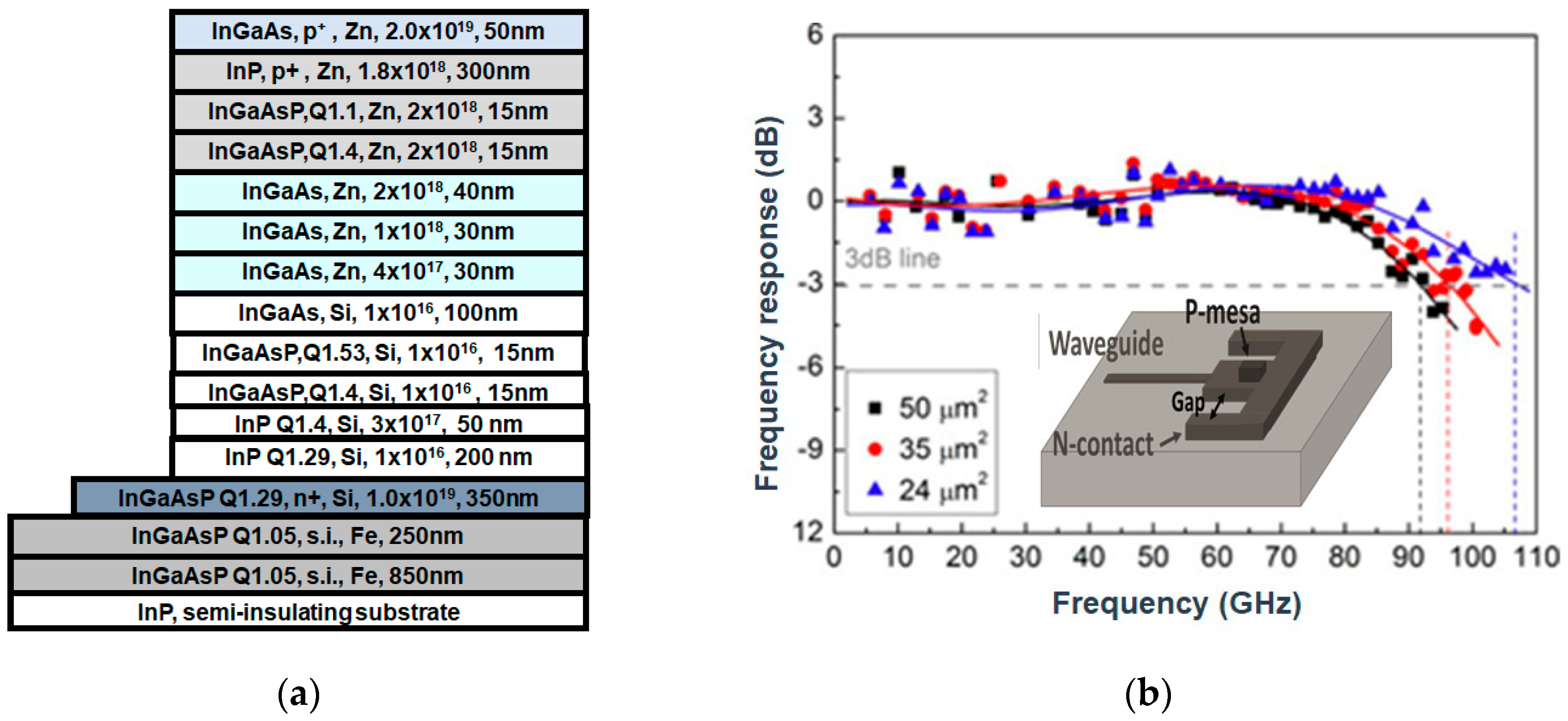
It is well-known that a decrease in the absorption layer thickness in order to reduce the carrier transit time, results in a lower responsivity in a normal incidence photodiode. For example, in the 100-GHz PD in ref. [12], the absorption layer thickness was 180 nm (the drift layer thickness was 300 nm) to enable carrier transit times below 4 ps, however, the responsivity was only 0.17 A/W. To circumvent this trade-off, waveguide structures that decouple photon absorption from carrier transport can be employed. To this end, we have developed evanescently coupled waveguide-integrated MUTC PDs. Figure 2a shows the epitaxial layer structure that was grown on top of the InGaAsP input optical waveguide on the InP substrate [9]. The InGaAs absorber includes a 100 nm-thick p-type doped layer and a 100 nm-thick lightly n-type doped layer. A graded doping was designed to create a built-in electric field to support carrier transport in the un-depleted absorber. The 200 nm-thick charge-compensated InP drift layer was incorporated to reduce the junction capacitance. Intermediate-bandgap InGaAsP layers were added to prevent carrier pile-up at the band barriers. A quaternary cliff layer was designed to help increase the electric field in the depleted absorber and thus support electron transport across the heterojunction discontinuity into the drift layer.
Evanescently-coupled MUTC PDs were fabricated on a three inch InGaAsP/InP wafer that was grown by metal-organic chemical vapor deposition. The fabrication process involved a double-mesa process using dry etching and was carried out in UVA’s clean room facilities [9].
The frequency responses of photodiodes with various areas are shown in Figure 2b. All three PDs had 3 dB bandwidths over 90 GHz and showed flat responses up to 80 GHz. The PD with an area of 24 μm2 had a bandwidth of over 105 GHz. For applications that require efficient light detection at high modulation frequencies, the photodiode bandwidth efficiency product is an important figure of merit, which was 29 GHz, 32 GHz and 38 GHz for 24 μm2, 35 μm2, and 50 μm2 PDs, respectively [9]. Waveguide photodiodes fabricated from the same wafer lot achieved an RF output power of 5 dBm at 120 GHz in ref. [14].
3. Integrated Photodiode-Antenna Emitters
Recently, significant research has been devoted to the integration of photodiodes with antennas, or microwave photonic wireless transmitters [15,16]. Due to the everlasting demand for high data rate wireless transmission, the low frequency bands are already too crowded to cope with the requirements. Higher frequency bands well into the range of millimeter-waves are needed to be deployed for next generation high data rate wireless networks. However, the hardware for the wireless data transmission at millimeter-wave frequency is far from being mature. The traditional way of implementing the hardware using electronic systems has its drawbacks, such as the high signal propagation loss inside coaxial cables, the limited bandwidth of electronics and the susceptibility to electromagnetic interference, which are incompatible with system operation at millimeter-wave frequencies. The realization of these systems using photonic techniques is advantageous, mainly due to the low-loss signal propagation in optical fibers, broad bandwidth of photonic components, and immunity to electromagnetic interference.
For a photonic wireless transmitter, the data is imposed on an optical carrier and transmitted to the antenna site through optical fiber. Then, the optical signals are converted to the electrical domain by a PD. Finally, the signals are broadcast to the users wirelessly by the antenna. The PD should maintain high speed at high optical input power in order to achieve sufficient radiated power, which is why the MUTC PD is well suited for this application.
Besides the PD performance, system integration is also an important factor. For reliable operation, the system needs to have high mechanical strength, good thermal dissipation, and carefully designed RF characteristics for optimal coupling between PD and antenna. Moreover, compact planar structures are preferred owing to their small footprint and ease of large system integration such as in phased arrays.
In the following sections, we describe integrated photodiode-antenna emitters for applications in the V- and W-bands. The effective isotropic radiated power (EIRP) is among the highest in the literature due to the high power-handling capability of the MUTC PD, and its careful integration with the antenna. V-band frequencies are of particular interest since the Federal Communications Commission allocated a 7 GHz unlicensed spectrum (57–64 GHz) for 60 GHz band communication [17]. At 100 GHz and above, a growing number of applications including high-capacity wireless communication, non-destructive sensing/imaging, and radio astronomy continue to motivate the development of photonic components [18].
3.1. Photonic Emitter at 60 GHz
Figure 3a shows the epitaxial layer structure of the MUTC PD that was designed for 60 GHz [19]. It includes a 400-nm-thick 1 × 1016 cm−3 n-type doped drift layer and an InGaAs absorbing region with a total thickness of 500 nm. The transit-time limited component of the bandwidth was estimated to be 85 GHz. The measured bandwidth and saturation power of a 10-μm diameter PD (no antenna) are shown in Figure 3b,c. The PD had a 3-dB bandwidth of 60 GHz while the 1-dB RF saturation power reached 16.7 and 14.3 dBm at 50 and 60 GHz, respectively.
A coplanar patch antenna was designed to be about half a wavelength long to resonate at 60 GHz [20]. While the CPW antenna feed was designed to be 50 Ω, a 100 μm-long high impedance (85 Ω) contact pad was integrated on the PD chip to compensate for parasitic capacitance. After the antenna was fabricated on an AlN submount, the MUTC-PD was integrated by flip-chip bonding (Figure 4).
The radiated power of the integrated photodiode-antenna emitters was measured using the setup shown in Figure 5. The optical RF signal was generated using an optical heterodyne setup. The radiation power was received in the far field using a commercial horn antenna and measured by a RF power meter.
The received radiation power versus frequency is shown in Figure 6a. The power at 15 mA average photocurrent amounts to −15 to −35 dBm between 50 to 75 GHz. Also shown in Figure 6a is the simulated radiation power using the circuit model shown in the inset of Figure 6a. The received RF power was calculated using Friis’ Equation [21] based on the radiated power, gain of transmitting (4.5 dBi) and receiving (15 dBi) antennas, and free-space loss (−43 dB). The simulation and experimental results agree with each other. The radiation power at 60 GHz versus the photocurrent is shown in Figure 6b. The 1-dB RF saturation power is −6.5 dBm at −5 V and 45 mA photocurrent. Using Friis’ equation, the effective radiated power is 20 dBm. According to the IEEE 802.16 standard [22], a minimum power of −46.2 dBm is required at the receiver for a QPSK-modulated signal at 60 GHz, which should be possible once a 25-dBi receiving antenna in 15 m distance from the integrated photodiode-antenna emitter is used.
3.2. Photonic Emitter at 100 GHz
For the W-band integrated photodiode-antenna emitter, a high-power MUTC PD with a bandwidth of 110 GHz was used [12]. Due to the high attenuation of millimeter-wave radiation in the atmosphere, an antenna with high directional gain is desired. Commercial horn antennas and Si lenses are typically used for this purpose. However, they are bulky and incompatible with large system integration. In ref. [23], a planar Vivaldi antenna with high directional gain of 5.5 dBi was used to be integrated with the MUTC PD.
In order to achieve high radiation power, the transition between the PD and the antenna needs to be carefully designed. It has been shown that impedance matching has a significant effect on the radiation power of integrated photonic emitters [24] and that maximum RF power can be extracted from the PD by conjugate impedance matching. In [25], a matching network was used to achieve conjugate matching between the MUTC PD and the Vivaldi antenna.
Figure 7 shows the integrated photonic emitter after the PD die was flip-chip bonded onto the antenna with a matching network on AlN.
In order to suppress distortions of the radiation pattern due to substrate modes, an AlN superstrate was placed on top of the antenna [25]. The scattering parameter S11 of 5-, 6-, and 14-µm-diameter PDs were measured and are shown in Figure 8 after de-embedding the RF pads. Also shown in Figure 8 is the S11 of the Vivaldi antenna with a matching network. Owing to the optimized matching network, the input impedance of the Vivaldi antenna is transformed close to the conjugate impedance of the 5- and 6-µm-diameter PDs, while it is far from the conjugate matching condition of the 14-µm-diameter PD.
The E-plane radiation power of the integrated photonic antenna was characterized in the far field using the setup shown in Figure 9.
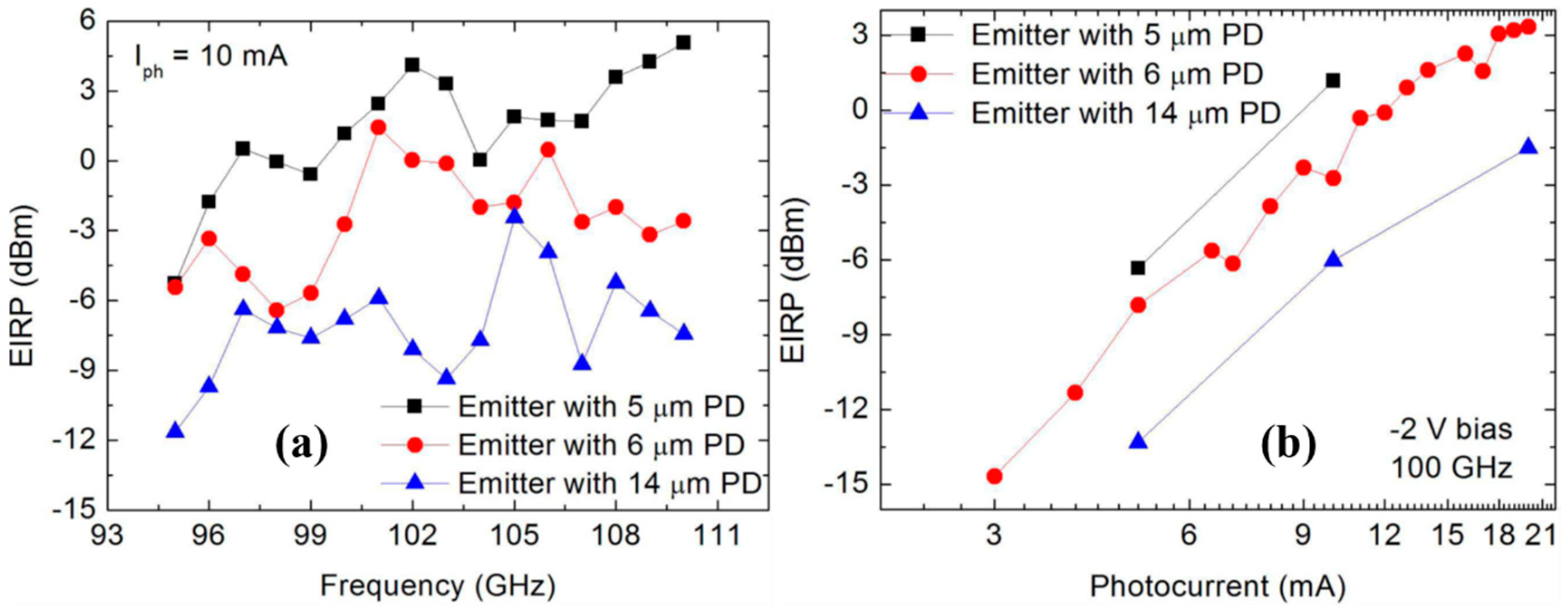
Devices with 5-, 6-, and 14-µm-diameter PDs were measured and their EIRP from 95 to 110 GHz are shown in Figure 10a. Photonic emitters with 5- and 6-µm-diameter PDs reached higher EIRP than the photonic emitter with the 14-µm-diameter PD, which can be explained by the larger PD junction capacitance and poor impedance matching. The photonic emitter with 5-µm-diameter PD reached 5 dBm at 110 GHz, and the -6-dB bandwidth for all three photonic emitters was 10 GHz. The fact that the EIRP varies across the measured frequency range might result from the varying impedance matching condition. The EIRP at 100 GHz as a function of photocurrent is shown in Figure 10b.
3.3. Summary of Results Reported in the Literature
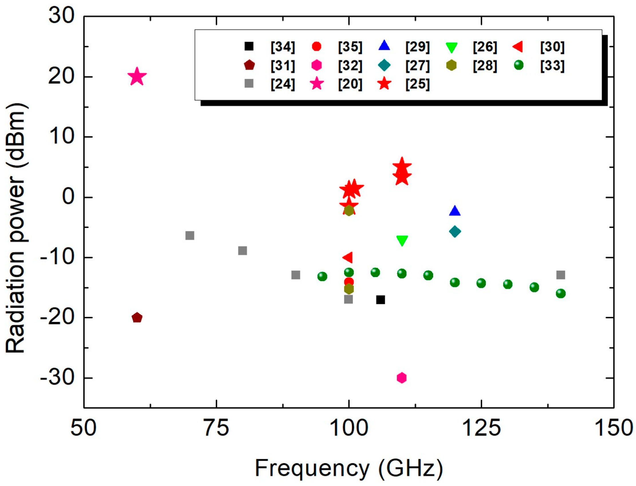
Figure 11 gives an overview of the radiation power of photonic emitters from 50 to 150 GHz that have been reported in the literature. In [26,27,28], a horn antenna with high directional gain was connected to the PDs. In refs. [27,29,30,31,32,33], either a Teflon or Si lens was used to improve the directional gain of the antenna. Planar antenna structures include Yagi [34,35], bow-tie [18,24], and slot [29,35], however, impedance matching between PD and antenna was not reported for these structures. In contrast, the integrated photonic emitters reported in refs. [23,25] have planar structures and include an impedance matching network. Due to the high-power handling capability of the MUTC PD, these integrated photodiode-antenna emitters have the highest radiation power, both, at 60 GHz, and 100 GHz.
4. High-Power Photodiodes on Si
The development of photonic integrated circuits on silicon has large technological and commercial significance, since it can leverage the mature Si CMOS technology to reduce the manufacturing costs. However, in order to achieve optoelectronic functionality at 1.55 μm wavelength, typically other materials have to be integrated on silicon. For PDs, the candidates include group III-V semiconductors and Germanium.
4.1. Heterogenous Photodiodes
Heterogeneous silicon photonics, i.e the integration of group III-V materials onto silicon, benefits from the mature Si processing technology, while fully exploiting the high-performance of III-V materials. Since bandgap-engineering is available in III-V semiconductors, complex photodiode heterostructures can be designed, which have been shown to enable high-power high-linearity analog applications [5]. To date, three approaches have been reported for the heterogeneous integration of III-V photodiodes on silicon: (i) molecular bonding [36], (ii) adhesive bonding [37], and (iii) III-V material growth on Si [38]. Previously, it has been demonstrated that molecular die and wafer bonding are technologies that combine different materials without compromising their properties. These approaches have produced high-performance photodiodes with a low dark current, high responsivity at 1.55 µm wavelength, high speed, and high power [39,40]. In [39], waveguide MUTC PDs were fabricated from an InGaAs/InP die that was wafer-bonded onto silicon-on-insulator (SOI). The PDs had an internal responsivity of 0.95 A/W, with a very low dark current of 10 nA (2.9 mA/cm2), a bandwidth of 48 GHz, and high RF output power of 12 dBm at 40 GHz. In ref. [40], this work was extended to waveguide photodiodes with a bandwidth of 65 GHz. Figure 12a,b shows the device structure and the measured frequency responses, respectively. Unlike some earlier work, an inverted photodiode layer stack was used, which resulted in the p-contact being on top after dye bonding. To enable efficient optical coupling from the silicon waveguide through the low-index InP drift layer into the absorber, the Si waveguide was designed to be 300 nm wide (inset of Figure 12b). It follows that the optical mode is no longer confined. Instead, it is pushed upwards into the active photodiode region. It should be noted, that the heterogeneous integration process, which allows changing the widths of the PD mesa and the Si waveguide independently, enabled this design. Responsivity and dark current were 0.84 A/W at 1.55 μm and 1 nA at −3 V, respectively. The output power was −2 dBm at 70 GHz for a PD with an area of 75 μm2 [40].
4.2. Ge-on-Si Photodiode Arrays
For monolithic integration, germanium-on-silicon has been widely investigated for near-infrared optoelectronics, and despite a lattice mismatch of 4%, Ge heterogeneous epitaxy on Si substrates has been successfully demonstrated with sufficiently low defect densities [41]. Compared to III-V growth on Si [42], Ge-on-Si is more compatible with the Si CMOS process. In addition, Ge can be directly grown on Si without buffer layers, which makes optical coupling between passive structures and Ge photodetectors easier. As a result, Ge-on-Si has become a well-developed platform for photonic integrated circuits [43]. Today, many foundries offer complete suites of technologies based on this platform, including the American Institute for manufacturing Integrated Photonics (AIM Photonics), IMEC, GlobalFoundries, Institute of Microelectronics (IME), STMicroelectronics, Taiwan Semiconductor Manufacturing Company (TSMC), and TowerJazz [44].
Ge-on-Si PDs with a low dark current, large bandwidth and high responsivity are well-developed in monolithic Si photonic platforms for digital applications [45,46,47], and large scale digital systems have been realized [48]. However, only a few Ge-on-Si PDs for high-power analog applications have been demonstrated. In addition to high responsivity and large bandwidth, PDs for microwave photonics applications should possess high-power handling capability and high linearity in order to achieve large RF gain and high spur-free dynamic range. For example, in order to achieve an RF link gain of 0 dB with a modulator with Vπ of 3 V, the photocurrent should be as high as 27 mA for an intensity-modulated direct detection link and 14 mA for a phase-modulated link. These photocurrents are much larger than the ones that typically occur in digital applications. The fact that the PDs need to maintain a large bandwidth and high linearity at these levels of photocurrents, puts stringent requirements on PDs in Si photonics.
Lack of material versatility limits the design freedom of epi-layers in monolithic Ge-on-Si PDs. To mitigate this drawback, PD arrays have been proposed. In [49], 8 Ge PDs were connected in a traveling-wave fashion and the optical signal was fed from both sides of the active region in order to enhance the power handling capability. In ref. [50], four Ge PDs were connected in parallel in a compact array to enhance the RF output power. The optical image and schematic of the PD array are shown in Figure 13a. The device layout was designed using the AIM Si photonics Process Design Kit (PDK) [51]. Three optical waveguide Y-junctions were used to equally split the input optical power to feed the four PDs. The outputs of the PDs were connected in parallel to the shared ground-signal-ground (GSG) pad on the top dielectric layer through vias. The device was fabricated on a multi project wafer run in AIM’s Si photonics foundry.
The I-V characteristics of the PD array are shown in Figure 13b. The dark current is as low as 0.3 μA at −2 V and 1 μA at −5 V bias. The PD array has a high external responsivity of 0.58 A/W at 1550 nm wavelength (no anti-reflection coating at the waveguide edge coupler) when measured with a lensed fiber with 3 μm spot size. The fiber-chip coupling loss was estimated to be 1.7 dB.
The frequency response of the PD array was measured at −5 V bias at various photocurrents from 1 mA to 20 mA. The results are shown in Figure 14a. The 3-dB bandwidth is 15 GHz up to a photocurrent of 15 mA and remains as high as 12 GHz at 20 mA photocurrent. The RF output power of the PD array was measured at the 3-dB bandwidth frequency under different reverse voltages. As shown in Figure 14b, the RF power increases with reverse voltage and begins to saturate above −5 V bias. The RF power and the saturation current at 1-dB compression are 7 dBm and 19 mA, respectively, under −7 V at 15 GHz.
In order to demonstrate the applicability of a Ge-on-Si PD array in a microwave photonics application, a balanced PD pair integrated with a Mach-Zehnder delay line interferometer (MZ DLI) was used to demodulate and detect a phase-modulated signal in an analog photonic link. The optical image and the schematic of the integrated receiver are shown in Figure 15. The optical input signal is fed through one of the vertical grating couplers and then split by a Y-junction. One arm includes a 1.4 mm-long silicon waveguide to delay the optical signal by 25 ps to allow for interferometric demodulation of the phase modulated signal. The demodulator worked at the quadrature point by adjusting the laser wavelength.
The RF gain of the phase-modulated link was measured using the setup shown in Figure 16a. A commercial optical phase modulator with a Vπ of 7 V was driven by a signal generator to modulate the phase of the optical carrier from the 1550 nm laser. The demodulated signal was recorded from a spectrum analyzer. The RF link gain versus frequency at different photocurrents is shown in Figure 16b. Also shown in the figure is the calculated link gain versus frequency according to [52]. The measurement agrees well with the theory once the 3-dB bandwidth of the balanced PD pair of 20 GHz was taken into account (blue curve). At 7 mA photocurrent per PD, the difference between the measurement (black curve) and the ideal model (red curve) increases, which indicates a reduction of the bandwidth of the balanced PDs due to saturation. A higher RF gain can be expected from traveling wave balanced PD arrays.
5. Conclusions
Figure 17 summarizes the RF output power versus frequency of PDs for high-power analog applications that have been reported in the literature. The green data points represent normal-incidence PDs onnative InP substrate. The RF output power reaches over 30 dBm at 10 GHz to 7 dBm at 100 GHz. Uniform light illumination, good thermal dissipation due to the flip-chip bonding on materials of high thermal conductivity, and advanced heterostructure designs yielded such high RF output power levels. The yellow data points represent the RF output power from waveguide PDs on native InP substrate. The output powers are lower than those of surface normal incident PDs due to the non-uniform light coupling from the waveguide into the absorber, which can cause localized space charge effects. The state-of-the-art performance of waveguide PDs on Si based on III-V materials is represented by the blue data points. Their RF output power reaches 17 dBm at 10 GHz and 2 dBm at 70 GHz. These waveguide PDs are integrated on Si by direct bonding. As a result, good thermal dissipation to the Si substrate can be expected, and output power levels similar to those of waveguide PDs on native InP are achieved. The high-power performance of monolithic Ge-on-Si PDs is represented by the red data points in Figure 17. To date, monolithic Ge-on-Si PD arrays have achieved high RF output power up to 40 GHz.
Author Contributions
K.S. and A.B equally contributed to the writing of the manuscript.
Conflicts of Interest
The authors declare no conflict of interest.
References
- Cox, C.H., III; Ackerman, E.I.; Betts, G.E.; Prince, J.L. Limits on the Performance of RF-Over-Fiber Links and Their Impact on Device Design. IEEE Trans. Microw. Theory Tech. 2006, 54, 906–920. [Google Scholar] [CrossRef]
- Williams, K.J.; Tulchinsky, D.A.; Boos, J.B.; Park, D.; Goetz, P.G. High Power Photodiode. In Proceedings of the LEOS Summer Topical Meetings, Quebec City, QC, Canada, 17–19 July 2006; pp. 50–51. [Google Scholar]
- Bai, J.; Shi, S.; Schneider, G.J.; Wilson, J.P.; Zhang, Y.; Pan, W.; Prather, D.W. Optically Driven Ultrawideband Phased Array with an Optical Interleaving Feed Network. IEEE Antennas Wirel. Propag. Lett. 2014, 13, 47–50. [Google Scholar]
- Baynes, F.N.; Quinlan, F.; Fortier, T.M.; Zhou, Q.; Beling, A.; Campbell, J.C.; Diddams, S.A. Attosecond timing in optical-to-electrical conversion. Optica 2015, 2, 141–146. [Google Scholar] [CrossRef]
- Yang, Z.; Xie, X.; Li, Q.; Campbell, J.C.; Beling, A. 20 GHz analog photonic link with 16 dB gain based on a high-power balanced photodiode. In Proceedings of the 2015 IEEE Photonics Conference (IPC), Reston, VA, USA, 4–8 October 2015; pp. 144–145. [Google Scholar]
- Ishibashi, T.; Shimizu, N.; Kodama, S.; Ito, H.; Nagatsuma, T.; Furuta, T. Uni-Traveling-Carrier Photodiodes. In Proceedings of the Ultrafast Electronics and Optoelectronics, Incline Village, NV, USA, 17 March 1997; Nuss, M., Bowers, J., Eds.; OSA Trends in Optics and Photonics Series (Optical Society of America, 1997), paper UC3. Volume 13, pp. 83–87. [Google Scholar]
- Kodama, S.; Ito, H. UTC-PD-based optoelectronic components for high-frequency and high-speed applications. IEICE Trans. Electron. 2007, 90, 429–435. [Google Scholar] [CrossRef]
- Ishibashi, T.; Furtua, T.; Fushimi, H.; Ito, H. Photoresponse characteristics of uni-traveling-carrier photodiodes. Proc. SPIE Int. Soc. Opt. Eng. 2001, 4283, 469–479. [Google Scholar]
- Li, Q.; Sun, K.; Li, K.; Yu, Q.; Runge, P.; Ebert, W.; Beling, A.; Campbell, J.C. Campbell High-Power Evanescently Coupled Waveguide MUTC Photodiode With >105-GHz Bandwidth. J. Lightwave Technol. 2017, 35, 4752–4757. [Google Scholar] [CrossRef]
- Li, N.; Sidhu, R.; Li, X.; Ma, F.; Demiguel, S.; Zhen, X.; Holmes, A.L.; Campbell, J.C.; Tulchinsky, D.A.; Williams, K.J. High-saturation-current InGaAs/InAlAs charge-compensated uni-traveling-carrier photodiode. Phys. Status Solidi (a) 2004, 201, 3037–3041. [Google Scholar] [CrossRef]
- Xie, X.; Zhou, Q.; Li, K.; Shen, Y.; Li, Q.; Yang, Z.; Beling, A.; Campbell, J.C. Improved power conversion efficiency in high performance photodiodes by flip chip on diamond. Optica 2014, 1, 429–435. [Google Scholar] [CrossRef]
- Li, Q.; Li, K.; Fu, Y.; Xie, X.; Yang, Z.; Beling, A.; Campbell, J.C. High-power flip-chip bonded photodiode with 110 GHz bandwidth. J. Lightwave Technol. 2016, 34, 2139–2144. [Google Scholar] [CrossRef]
- Morgan, J.S.; Sun, K.; Li, Q.; Estrella, S.; Woodson, M.; Hay, K.; Mashanovitch, M.; Beling, A. High-Power Flip-Chip Bonded Modified Uni-Traveling Carrier Photodiodes with −2.6 dBm RF Output Power at 160 GHz. In Proceedings of the 2018 IEEE Photonics Conference (IPC), Reston, VA, USA, 30 September–4 October 2018; pp. 1–2. [Google Scholar] [CrossRef]
- Zhou, G.; Runge, P.; Keyvaninia, S.; Seifert, S.; Ebert, W.; Mutschall, S.; Seeger, A.; Li, Q.; Beling, A. High-Power InP-Based Waveguide Integrated Modified Uni-Traveling-Carrier Photodiodes. J. Lightwave Technol. 2017, 35, 717–721. [Google Scholar] [CrossRef]
- Park, C.; Rappaport, T.S. Short-range wireless communications for next-generation networks: UWB, 60 GHz millimeter-wave WPAN, and ZigBee. IEEE Wirel. Commun. 2007, 14, 70–78. [Google Scholar] [CrossRef]
- Stohr, A.; Babiel, S.; Cannard, P.J.; Charbonnier, B.; van Dijk, F.; Fedderwitz, S.; Moodie, D.; Pavlovic, L.; Ponnampalam, L.; Renaud, C.C.; et al. Millimeter-wave photonic components for broadband wireless systems. IEEE Trans. Microw. Theory Tech. 2010, 58, 3071–3082. [Google Scholar] [CrossRef]
- Amendment of Parts 2, 15 and 97 of the Comission’s Rules to Permit Use of Radio Frequencies above 40 GHz for New Radio Applications; Federal Communications Commission: Washington, DC, USA, 1995.
- Stöhr, A. Pushing the boundaries. IEEE Microw. Mag. 2009, 10, 106–115. [Google Scholar] [CrossRef]
- Zhou, Q.; Cross, A.S.; Beling, A.; Fu, Y.; Lu, Z.; Campbell, J.C. High-power V-band InGaAs/InP photodiodes. IEEE Photonics Technol. Lett. 2013, 25, 907–909. [Google Scholar] [CrossRef]
- Li, K.; Xie, X.; Li, Q.; Shen, Y.; Woodsen, M.E.; Yang, Z.; Beling, A.; Campbell, J.C. High-power photodiode integrated with coplanar patch antenna for 60-GHz applications. IEEE Photonics Technol. Lett. 2015, 27, 650–653. [Google Scholar] [CrossRef]
- Friis, H.T. A note on a simple transmission formula. Proc. IRE 1946, 34, 254–256. [Google Scholar] [CrossRef]
- IEEE Standard for Local and Metropolitan Area Networks, Part 16: Air Interface for Fixed Broadband Wireless Access Systems; IEEE Standard 802.162004; IEEE: New York, NY, USA, 2004.
- Moody, J.; Sun, K.; Li, Q.; Beling, A.; Bowers, S.M. A Vivaldi antenna based W-band MUTC photodiode driven radiator. In Proceedings of the IEEE International Topical Meeting on Microwave Photonics (MWP), Long Beach, CA, USA, 31 October–3 November 2016; pp. 217–220. [Google Scholar]
- Natrella, M.; Liu, C.P.; Graham, C.; van Dijk, F.; Liu, H.; Renaud, C.C.; Seeds, A.J. Modelling and measurement of the absolute level of power radiated by antenna integrated THz UTC photodiodes. Opt. Express 2016, 24, 11793–11807. [Google Scholar] [CrossRef]
- Sun, K.; Moody, J.; Li, Q.; Bowers, S.M.; Beling, A. High power integrated photonic W-band emitter. IEEE Trans. Microw. Theory Tech. 2011, 59, 978–986. [Google Scholar] [CrossRef]
- Huggard, P.G.; Ellison, B.N.; Shen, P.; Gomes, N.J.; Davies, P.A.; Shillue, W.; Vaccari, A.; Payne, J.M. Generation of millimetre and sub-millimetre waves by photomixing in 1.55 μm wavelength photodiode. Electron. Lett. 2002, 38, 327–328. [Google Scholar] [CrossRef]
- Hirata, A.; Minotani, T.; Nagatsuma, T. A 120-GHz microstrip antenna monolithically integrated with a photodiode on Si. Jpn. J. Appl. Phys. 2002, 41, 1390–1394. [Google Scholar] [CrossRef]
- Rouvalis, E.; Renaud, C.C.; Moodie, D.G.; Robertson, M.J.; Seeds, A.J. Continuous wave terahertz generation from ultra-fast InP-based photodiodes. IEEE Trans. Microw. Theory Tech. 2012, 60, 509–517. [Google Scholar] [CrossRef]
- Hirata, A.; Ishii, H.; Nagatsuma, T. Design and characterization of a 120-GHz millimeter-wave antenna for integrated photonic transmitters. IEEE Trans. Microw. Theory Tech. 2001, 49, 2157–2162. [Google Scholar] [CrossRef]
- Stohr, A.; Malcoci, A.; Sauerwald, A.; Mayorga, I.C.; Gusten, R.; Jager, D.S. Ultra-wide-band traveling-wave photodetectors for photonic local oscillators. J. Lightwave Technol. 2003, 21, 3062–3070. [Google Scholar] [CrossRef]
- Shi, J.-W.; Wu, Y.-S.; Lin, Y.-S. Near-ballistic uni-traveling carrier photodiode-based V-band optoelectronic mixers with internal up-conversion-gain, wide modulation bandwidth, and very high operation current performance. IEEE Photonics Technol. Lett. 2008, 20, 939–941. [Google Scholar] [CrossRef]
- Hirata, A.; Nagatsuma, T.; Yano, R.; Ito, H.; Furuta, T.; Hirota, Y.; Ishibashi, T.; Matsuo, H.; Ueda, A.; Noguchi, T.; Sekimoto, Y.; Ishiguro, M.; Matsuura, S. Output power measurement of photonic millimeter-wave and sub-millimeter-wave emitter at 100–800 GHz. Electron. Lett. 2002, 38, 798–800. [Google Scholar] [CrossRef]
- Hirata, A.; Harada, M.; Nagatsuma, T. 120-GHz wireless link using photonic techniques for generation, modulation, and emission of millimeter-wave signals. J. Lightwave Technol. 2003, 21, 2145–2153. [Google Scholar] [CrossRef] [Green Version]
- Wu, Y.-S.; Chen, N.-W.; Shi, J.-W. A W-band photonic transmitter/mixer based on high-power near-ballistic uni-traveling-carrier photodiode (NBUTC-PD). IEEE Photonics Technol. Lett. 2008, 20, 1799–1801. [Google Scholar] [CrossRef]
- Shi, J.-W.; Kuo, F.M.; Wu, Y.-S.; Chen, N.-W.; Shih, P.-T.; Lin, C.-T.; Jiang, W.-J.; Wong, E.-Z.; Chen, C.; Chi, S. A W-band photonic transmitter-mixer based on high power near-ballistic uni-traveling-carrier photodiodes for BPSK and QPSK data transmission under bias modulation. IEEE Photonics Technol. Lett. 2009, 20, 1039–1041. [Google Scholar] [CrossRef]
- Chang, H.; Kuo, Y.; Chen, H.; Jones, R.; Barkai, A.; Paniccia, M.J.; Bowers, J.E. Integrated Triplexer on Hybrid Silicon Platform. In Proceedings of the Optical Fiber Communication Conference, San Diego, CA, USA, 21–25 March 2010. [Google Scholar]
- Liang, D.; Roelkens, G.; Baets, R.; Bowers, J.E. Hybrid Integrated Platforms for Silicon Photonics. Materials 2010, 3, 1782–1802. [Google Scholar] [CrossRef] [Green Version]
- Geng, Y.; Feng, S.; Poon, A.; Lau, K. High-speed InGaAs photodetectors by selective-area MOCVD toward optoelectronic integrated circuits. IEEE J. Sel. Top. Quantum Electron. 2014, 20, 3801807. [Google Scholar] [CrossRef]
- Xie, X.; Zhou, Q.; Norberg, E.; Jacob-Mitos, M.; Chen, Y.; Ramaswamy, A.; Fish, G.; Bowers, J.E.; Campbell, J.C.; Beling, A. Heterogeneously Integrated Waveguide-Coupled Photodiodes on SOI with 12 dBm Output Power at 40 GHz. In Proceedings of the 2015 Optical Fiber Communications Conference and Exhibition (OFC), Los Angeles, CA, USA, 22–26 March 2015; pp. 1–3, Postdeadline Paper. [Google Scholar]
- Wang, Y.; Wang, Z.; Yu, Q.; Xie, X.; Posavitz, T.; Jacob-Mitos, M.; Ramaswamy, A.; Norberg, E.J.; Fish, G.A.; Beling, A. High-Power Photodiodes With 65 GHz Bandwidth Heterogeneously Integrated onto Silicon-on-Insulator Nano-Waveguides. IEEE J. Sel. Top. Quantum Electron. 2018, 24, 1–6. [Google Scholar] [CrossRef]
- Michel, J.; Liu, J.; Kimerling, L.C. High-performance Ge-on-Si photodetectors. Nat. Photonics 2010, 4, 527–534. [Google Scholar] [CrossRef]
- Sun, K.; Jung, D.; Shang, C.; Liu, A.; Morgan, J.; Zang, J.; Li, Q.; Klamkin, J.; Bowers, J.E.; Beling, A. Low dark current III–V on silicon photodiodes by heteroepitaxy. Opt. Express 2018, 26, 13605–13613. [Google Scholar] [CrossRef] [PubMed]
- Stojanović, V.; Ram, R.J.; Popović, M.; Lin, S.; Moazeni, S.; Wade, M.; Sun, C.; Alloatti, L.; Atabaki, A.; Pavanello, F.; et al. Monolithic silicon-photonic platforms in state-of-the-art CMOS SOI processes. Opt. Express 2018, 26, 13106–13121. [Google Scholar] [CrossRef] [PubMed]
- Liu, A.Y.; Bowers, J.E. Photonic integration with epitaxial III-V on silicon. IEEE J. Sel. Top. Quantum Electron. 2018, 24, 6000412. [Google Scholar] [CrossRef]
- Lee, J.; Cho, S.; Choi, W. An equivalent circuit model for a Ge waveguide photodetector on Si. IEEE Photonics Technol. Lett. 2016, 28, 2435–2438. [Google Scholar] [CrossRef]
- Su, Z.; Hosseini, E.S.; Timurdogan, E.; Sun, J.; Moresco, M.; Leake, G.; Adam, T.N.; Coolbaugh, D.D.; Watts, M.R. Whispering gallery germanium-on-silicon photodetector. Opt. Lett. 2017, 42, 2878–2881. [Google Scholar] [CrossRef] [PubMed]
- Byrd, M.J.; Timurdogan, E.; Su, Z.; Poulton, C.V.; Fahrenkopf, N.M.; Leake, G.; Coolbaugh, D.D.; Watts, M.R. Mode-evolution-based coupler for high saturation power Ge-on-Si photodetectors. Opt. Lett. 2017, 42, 851–854. [Google Scholar] [CrossRef]
- Sun, C.; Wade, M.T.; Lee, Y.; Orcutt, J.S.; Alloatti, L.; Georgas, M.S.; Waterman, A.S.; Shainline, J.M.; Avizienis, R.R.; Lin, S.; et al. Single-chip microprocessor that communicates directly using light. Nature 2015, 528, 534–538. [Google Scholar] [CrossRef] [Green Version]
- Chang, C.; Sinsky, J.H.; Dong, P.; Valicourt, G.; Chen, Y. High-power dual-fed traveling wave photodetector circuits in silicon photonics. Opt. Express 2015, 23, 22857–22866. [Google Scholar] [CrossRef]
- Sun, K.; Costanzo, R.; Tzu, T.; Yu, Q.; Bowers, S.M.; Beling, A. Ge-on-Si Waveguide Photodiode Array for High-Power Applications. In Proceedings of the 2018 IEEE Photonics Conference (IPC), Reston, VA, USA, 30 September–4 October 2018. Paper MB2.3. [Google Scholar]
- AIM Photonics. Available online: http://www.aimphotonics.com (accessed on 10 February 2019).
- Yang, Z.; Yu, Q.; Zang, J.; Campbell, J.C.; Beling, A. Phase-modulated analog photonic link with a high-power high-linearity photodiode. J. Lightwave Technol. 2018, 36, 3805–3814. [Google Scholar] [CrossRef]
- Li, Z.; Pan, H.; Chen, H.; Beling, A.; Campbell, J.C. High-Saturation-Current Modified Uni-Traveling-Carrier Photodiode with Cliff Layer. IEEE J. Quantum Electron. 2010, 46, 626–632. [Google Scholar] [CrossRef]
- Li, K.; Xie, X.; Zhou, Q.; Beling, A.; Campbell, J.C. High Power 20-GHz Photodiodes with Resonant Microwave Circuits. IEEE Photonics Technol. Lett. 2014, 26, 1303–1306. [Google Scholar] [CrossRef]
- Wang, X.; Duan, N.; Chen, H.; Campbell, J.C. InGaAs–InP Photodiodes with High Responsivity and High Saturation Power. IEEE Photonics Technol. Lett. 2007, 19, 1272–1274. [Google Scholar] [CrossRef]
- Li, N.; Li, X.; Demiguel, S.; Zheng, X.; Campbell, J.C.; Tulchinsky, D.A.; Williams, K.J.; Isshiki, T.D.; Kinsey, G.S.; Sudharsansan, R. High-saturation-current charge-compensated InGaAs-InP uni-traveling-carrier photodiode. IEEE Photonics Technol. Lett. 2004, 16, 864–866. [Google Scholar] [CrossRef]
- Sakai, K.; Ishimura, E.; Nakaji, M.; Itakura, S.; Hirano, Y.; Aoyagi, T. High-current back-illuminated partially depleted-absorber p-i-n photodiode with depleted nonabsorbing region. IEEE Trans. Microw. Theory Tech. 2010, 58, 3154–3160. [Google Scholar] [CrossRef]
- Rouvalis, E.; Muller, P.; Tromme, D.; Stephan, J.; Steffan, A.G.; Unterborsch, U. A 1×4 MMI-integrated high-power waveguide photodetector. In Proceedings of the 2013 International Conference on Indium Phosphide and Related Materials (IPRM), Kobe, Japan, 19–23 May 2013; pp. 1–2. [Google Scholar]
- Achouche, M.; Magnin, V.; Harari, J.; Lelarge, F.; Derouin, E.; Jany, C.; Carpentier, D.; Blache, F.; Decoster, D. High performance evanescent edge coupled waveguide unitraveling-carrier photodiodes for >40-gb/s optical receivers. IEEE Photonics Technol. Lett. 2004, 16, 584–586. [Google Scholar] [CrossRef]
- Anagnosti, M.; Caillaud, C.; Blache, F.; Jorge, F.; Angelini, P.; Paret, J.F.; Achouche, M. Optimized high speed UTC photodiode for 100 Gbit/s applications. IEEE J. Sel. Top. Quantum Electron. 2014, 20, 3801107. [Google Scholar] [CrossRef]
- Demiguel, S.; Li, N.; Li, X.; Zheng, X.; Kim, J.; Campbell, J.C.; Lu, H.; Anselm, A. Very high-responsivity evanescently coupled photodiodes integrating a short planar multimode waveguide for high-speed applications. IEEE Photonics Technol. Lett. 2003, 15, 1761–1763. [Google Scholar] [CrossRef]
- Wu, Y.S.; Shi, J.W.; Chiu, P.H.; Lin, W. High-performance dual-step evanescently coupled uni-traveling-carrier photodiodes. IEEE Photonics Technol. Lett. 2007, 19, 1682–1684. [Google Scholar] [CrossRef]
- Zhou, G.; Ebert, W.; Mutschall, S.; Seeger, A.; Runge, P.; Li, Q.; Beling, A. High-power waveguide integrated modified uni-traveling-carrier (UTC) photodiode with 5 dBm RF output power at 120 GHz. In Proceedings of the 2016 Optical Fiber Communications Conference and Exhibition (OFC), Anaheim, CA, USA, 20–24 March 2016. Paper Tu2D.3. [Google Scholar]
- Zhou, G.; Runge, P.; Lankes, S.; Seeger, A.; Schell, M. Waveguide integrated pin-photodiode array with high power and high linearity. In Proceedings of the 2015 International Topical Meeting on Microwave Photonics (MWP), Paphos, Cyprus, 26–29 October 2015; pp. 1–4. [Google Scholar]
- Shi, J.; Wu, Y.; Wu, C.; Chiu, P.; Hong, C. High-speed, high-responsivity, and high-power performance of near-ballistic uni-traveling-carrier photodiode at 1.55-μm wavelength. IEEE Photonics Technol. Lett. 2005, 17, 1929–1931. [Google Scholar] [CrossRef]
- Beling, A.; Cross, A.S.; Piels, M.; Peters, J.; Zhou, Q.; Bowers, J.E.; Campbell, J.C. InP-based waveguide photodiodes heterogeneously integrated on silicon-on-insulator for photonic microwave generation. Opt. Express 2013, 21, 25901–25906. [Google Scholar] [CrossRef] [PubMed]
- Xie, X.; Zhou, Q.; Norberg, E.; Jacob-Mitos, M.; Yang, Z.; Chen, Y.; Ramaswamy, A.; Fish, G.; Campbell, J.C.; Beling, A. High-power heterogeneously integrated waveguide-coupled balanced photodiodes on silicon-on-insulator. In Proceedings of the 2015 IEEE Photonics Conference (IPC), Reston, VA, USA, 4–8 October 2015; pp. 468–469. [Google Scholar]
- Hulme, J.; Kennedy, M.J.; Chao, R.; Komljenovic, T.; Shi, J.; Bowers, J.E. Heterogeneously integrated InP based evanescently-coupled high-speed and high-power p-i-n photodiodes on silicon-on-insulator (SOI) substrate. In Proceedings of the 2016 IEEE International Topical Meeting on Microwave Photonics (MWP), Long Beach, CA, USA, 31 October–3 November 2016; pp. 233–236. [Google Scholar]
- Piels, M.; Bowers, J.E. 40 GHz Si/Ge Uni-Traveling Carrier Waveguide Photodiode. J. Lightwave Technol. 2014, 32, 3502–3508. [Google Scholar] [CrossRef]
- Ramaswamy, A.; Piels, M.; Nunoya, N.; Yin, T.; Bowers, J.E. High power silicon-germanium photodiodes for microwave photonic applications. IEEE Trans. Microw. Theory Tech. 2010, 58, 3336–3343. [Google Scholar] [CrossRef]
Figure 1.
(a) Photodiode (PD) die on submount after flip-chip bonding. (b) Radio frequency (RF) output power and compression at 160 GHz of modified uni-traveling carrier photodiodes (MUTC-PDs) with different diameters.
Figure 1.
(a) Photodiode (PD) die on submount after flip-chip bonding. (b) Radio frequency (RF) output power and compression at 160 GHz of modified uni-traveling carrier photodiodes (MUTC-PDs) with different diameters.

Figure 2.
(a) Layer stack of waveguide MUTC PD; doping concentrations are given in cm−3 (b) Frequency responses of PDs with different active areas; inset: schematic layout.
Figure 2.
(a) Layer stack of waveguide MUTC PD; doping concentrations are given in cm−3 (b) Frequency responses of PDs with different active areas; inset: schematic layout.

Figure 3.
(a) Epitaxial layer design of MUTC-PD. (b) Measured bandwidth of 10-µm-diameter MUTC-PD. The inset shows a microscopic image of the fabricated device. (c) RF output power measurement of the MUTC-PD.
Figure 3.
(a) Epitaxial layer design of MUTC-PD. (b) Measured bandwidth of 10-µm-diameter MUTC-PD. The inset shows a microscopic image of the fabricated device. (c) RF output power measurement of the MUTC-PD.

Figure 4.
Schematic and optical image of the integrated photodiode-antenna emitter. A 50-Ω transmission line connects the patch antenna (829 μm × 2668 μm) and the flip-chip bonded MUTC PD chip.
Figure 4.
Schematic and optical image of the integrated photodiode-antenna emitter. A 50-Ω transmission line connects the patch antenna (829 μm × 2668 μm) and the flip-chip bonded MUTC PD chip.

Figure 5.
Experimental setup for measuring the radiation power at V-band. EDFA: erbium doped fiber amplifier, Att.: optical attenuator.
Figure 5.
Experimental setup for measuring the radiation power at V-band. EDFA: erbium doped fiber amplifier, Att.: optical attenuator.

Figure 6.
(a) Measured and simulated received RF power from the photonic emitter at 5 V bias voltage and 15 mA photocurrent. The inset shows the circuit model used to simulate the RF power. (b) RF received power versus photocurrent at 5 V bias and 60 GHz frequency.
Figure 6.
(a) Measured and simulated received RF power from the photonic emitter at 5 V bias voltage and 15 mA photocurrent. The inset shows the circuit model used to simulate the RF power. (b) RF received power versus photocurrent at 5 V bias and 60 GHz frequency.

Figure 7.
(a) Optical image and (b) 3-D schematic of the integrated photonic emitter.

Figure 8.
Scattering parameters of 5-, 6-, and 14-µm-diameter PDs and the Vivaldi antenna with a matching network.
Figure 8.
Scattering parameters of 5-, 6-, and 14-µm-diameter PDs and the Vivaldi antenna with a matching network.

Figure 9.
Experimental setup for measuring the radiation power of the photonic emitter at W-band. LO: local oscillator. The distance between photonic emitter and horn antenna was 60 cm.
Figure 9.
Experimental setup for measuring the radiation power of the photonic emitter at W-band. LO: local oscillator. The distance between photonic emitter and horn antenna was 60 cm.

Figure 10.
(a) Effective isotropic radiated power (EIRP) of the integrated photonic emitters with 5-, 6-, and 14-µm-diameter PDs at 10-mA photocurrent from 95 to 110 GHz. (b) EIRP at 100 GHz as a function of average photocurrent.
Figure 10.
(a) Effective isotropic radiated power (EIRP) of the integrated photonic emitters with 5-, 6-, and 14-µm-diameter PDs at 10-mA photocurrent from 95 to 110 GHz. (b) EIRP at 100 GHz as a function of average photocurrent.

Figure 11.
Radiation power of integrated photonic emitters reported in the literature.

Figure 12.
(a) Device structure of heterogeneous MUTC PD on silicon-on-insulator (SOI); (b) Measured frequency responses for PDs with different area. The inset shows a schematic view of the PD.
Figure 12.
(a) Device structure of heterogeneous MUTC PD on silicon-on-insulator (SOI); (b) Measured frequency responses for PDs with different area. The inset shows a schematic view of the PD.

Figure 13.
(a) Optical image and schematic of the PD array, and (b) I-V characteristics.

Figure 14.
(a) Frequency responses of PD array at different photocurrents. (b) RF output power and compression of the PD array at 15 GHz.
Figure 14.
(a) Frequency responses of PD array at different photocurrents. (b) RF output power and compression of the PD array at 15 GHz.

Figure 15.
Optical image and schematic of the interferometric demodulator.

Figure 16.
(a) Phase-modulated link gain measurement setup. (b) Measured and calculated RF gain spectra of the phase-modulated link at 2 and 7 mA photocurrent for each PD.
Figure 16.
(a) Phase-modulated link gain measurement setup. (b) Measured and calculated RF gain spectra of the phase-modulated link at 2 and 7 mA photocurrent for each PD.

Figure 17.
RF output power versus frequency of PDs for high-power analog applications reported in the literature. Green: normal-incidence PDs on native InP substrate; orange: waveguide PDs on native InP substrate; blue: integrated III-V waveguide PDs on Si; red: integrated Ge waveguide PDs on Si [9,11,12,19,39,40,49,50,53,54,55,56,57,58,59,60,61,62,63,64,65,66,67,68,69,70].

© 2019 by the authors. Licensee MDPI, Basel, Switzerland. This article is an open access article distributed under the terms and conditions of the Creative Commons Attribution (CC BY) license (http://creativecommons.org/licenses/by/4.0/).
Share and Cite
MDPI and ACS Style
Sun, K.; Beling, A. High-Speed Photodetectors for Microwave Photonics. Appl. Sci. 2019, 9, 623. https://doi.org/10.3390/app9040623
AMA Style
Sun K, Beling A. High-Speed Photodetectors for Microwave Photonics. Applied Sciences. 2019; 9(4):623. https://doi.org/10.3390/app9040623
Chicago/Turabian StyleSun, Keye, and Andreas Beling. 2019. "High-Speed Photodetectors for Microwave Photonics" Applied Sciences 9, no. 4: 623. https://doi.org/10.3390/app9040623
Note that from the first issue of 2016, this journal uses article numbers instead of page numbers. See further details here.