Article

Low-Cost CuIn1−xGaxSe2 Ultra-Thin Hole-Transporting Material Layer for Perovskite/CIGSe Heterojunction Solar Cells

1
Institute of Electro-Optical Engineering, Green Technology Research Center, Department of Electronic Engineering, Chang Gung University, Chang Gung Memorial Hospital, Taoyuan 333, Taiwan
2
Department of Electro-Optical Engineering, National Taipei University of Technology, Taipei 106, Taiwan
3
Department of Quantum Technologies, Wroclaw University of Science Technology, Wroclaw 50-370, Poland
*
Author to whom correspondence should be addressed.
Appl. Sci. 2019, 9(4), 719; https://doi.org/10.3390/app9040719
Submission received: 17 December 2018 / Revised: 14 February 2019 / Accepted: 15 February 2019 / Published: 19 February 2019
(This article belongs to the Special Issue CIGS Thin Films and Solar Cells)

Abstract

:
This paper presents a new type of solar cellwith enhanced optical-current characteristics using an ultra-thin CuIn1−xGaxSe2 hole-transporting material (HTM) layer (<400 nm). The HTM layer was between a bi-layer Mo metal-electrode and a CH3NH3PbI3 (MAPbI3) perovskite active absorbing material. It promoted carrier transportand led to an improved device with good ohmic-contacts. The solar cell was prepared as a bi-layer Mo/CuIn1−xGaxSe2/perovskite/C60/Ag multilayer of nano-structures on an FTO (fluorine-doped tin oxide) glass substrate. The ultra-thin CuIn1−xGaxSe2 HTM layers were annealed at various temperatures of 400, 500, and 600 °C. Scanning electron microscopy studies revealed that the nano-crystal grain size of CuIn1−xGaxSe2 increased with the annealing temperature. The solar cell results show an improved optical power conversion efficiency at ~14.2%. The application of the CuIn1−xGaxSe2 layer with the perovskite absorbing material could be used for designing solar cells with a reduced HTM thickness. The CuIn1−xGaxSe2 HTM has been evidenced to maintain a properopen circuit voltage, short-circuit current density and photovoltaic stability.

1. Introduction

Hybrid organic-inorganic perovskite materials exhibit the advantages of easy fabrication, a large absorption coefficient, an adjustable energy band gap, high carrier mobility, and a long charge carrier diffusion length [1,2,3,4]. Metal halide-based perovskite solar cells (PSCs) have aimed for a better power conversion efficiency (PCE) for the next generationof photovoltaics [5,6,7].It should be pointed out that even if a lot of effort has been spent on the development of novel alternative solar cells like quantum dot solar cells [8] and single-material organic solar cells [9], perovskite-like solar cells are the most promising type of photovoltaic devices. To comprehend the green renewable energy demand, not only the cost-effectiveness of photovoltaic systems but also the expansion of its installation locations should be carefully established. Since the utility market facility has to regulate its growth rate, building-integrated photovoltaics is a potential candidate to solve such green renewable energy expectation.
In recent years, organic-inorganic hybrid substances, the remarkably dictated perovskite family, has shown great distinction for field-effect solar cells [10,11]. Lately, the PCE of lead halide perovskite (CH3NH3PbX3, X = Cl, Br, I)–based thin-film photovoltaic devices reached 22% [12,13,14,15,16]. The organic metal halide material has excellent performance for solarphoton harvesting due to its low energy band gap and large excitation diffusion length [17,18]. The optical energy band gap of organic metal perovskite (CH3NH3PbI3; MAPbI3) is ~1.56 eV. Consequently, this material benefits from efficient carrier generation and transportation to electrodes that can harvest sunlight radiation fromthe ultra-violet to infrared region. The diffusion length is more than one micrometer in the mixed halide perovskite [18]. Miyasaka et al. have investigated an organometal halide perovskite solar cell with a mesoporous TiO2. They used a CH3NH3PbI3 and CH3NH3PbBr3 nano-crystal material as absorbers, achieving an efficiency of 3.8% [19]. In 2012, Park and Gratzel et al. researched a complete solid-state perovskite solar cell withan FTO (fluorine-tin-oxide)/mesoporous TiO2/perovskite/2,2′,7,7′-tetrakis(N,N-di-p-methoxyphenyl-amino),9,9′spirobifluorene(SpiroOMeTAD)/gold structure, achieving an efficiency of 9% [20]. One year later, the first unique inverted planar composition nano-structure of a perovskite solar cell was announced and a similar nano-structure device was used in other organic perovskite solar cells [21]. This inverted nano-structure was fabricated on ITO (indium-tin-oxide)/poly(3,4-ethylene-dioxythiophene):poly(styrene-sulfonate) (PEDOT:PSS)/perovskite/(6,6)phenyl-C61-butyric-acid-methylester(PCBM)/silver, and PEDOT:PSS was used as the hole-transporting material(HTM). However, the traditional hole-transporting material of PEDOT:PSS is acidic, which can erode ITO and decrease the reliability of the perovskite solar cells [22,23]. Further investigations into the efficiency are still required for solar cells using other thin film materials, such as CdTe and CuIn1−xGaxSe2 [24].
Lately, Christians et al. evaluateda film interface-related reducing mechanism and improved the PCE stability of small-area solar cells [25]. Photovoltaic technology has showncontinuous improvement, withenhanced device stability and improved cell durability. The future prospects areindeed obvious for the renewable energy realm [26]. The stability requirements can be established by solar cell devices with a unique combination of material composition and device structure, toward cell efficiency, scalability, and durability [27]. Usually, FTO is used to replace ITO asthe transparent conducting oxide (TCO). The TCO is deposited on top of a glass substrate, such as in dye-sensitized solar cells and perovskite-based solar cells. The ITO electrical conductivity can be reduced in the presenceof oxygen at a relatively high temperature, such as around 500 °C. However, FTO is much more stable under a heat annealing environment. In addition, FTO has been distinguished for its use in numerous multi-structure photovoltaics and nano-structured devices [28,29].
Moreover, few investigators have studied metal-selenide as a carrier-transporting material for perovskite photovoltaic devices [30,31]. The metal-selenide material has attracted significant attention due to its outstanding optical properties and electric characteristics. Moreover, the energy band gap can be adjusted between 1.0 and 1.7 eV by varying the In:Ga ratio [32]. This also provides the possibility for tandem solar cells. The traditional standard thickness of CuIn1−xGaxSe2 absorber layer has been about 2–3 μm [33,34,35]. It is desirable to thin down the absorber layer’s thickness to below 1 μm. This would improve recombination at the back contact layer [36,37]. The recombination can be decreased by changing the In:Ga ratio toward the back contact layer, directing to a beneficial electron reaction and reducing the active absorber layer thickness to essentially decrease light absorption. Nevertheless, light trapping in CuIn1−xGaxSe2 ultra-thin solar cellsfaces challenges in crystallization growth and parasitic photon absorption at the Mo back metal-electrode contact layer. The absorption loss at the back contact layer should be considered for CuIn1−xGaxSe2 solar cell before its application in advanced photovoltaic devices [38,39].
Even now, CuIn1−xGaxSe2 thin-films are one of the most promising materials for photovoltaic devices because of their high solar photon absorption coefficient and direct energy band gap. They also exhibit a high conversion efficiency on various flexible substrates [39,40]. A small contact resistance between the metallic film and the optical absorber film is inevitable, as the contact resistance adds toa serial resistance. The Schottky barrier has been reported with a height of approximately 0.8 eV for the p-doped CuInSe2 (011)/Mo metal-contact film [41]. The molybdenum-diselenide (MoSe2) film has significant effects on the behavior of the Mo/CuIn1−xGaxSe2 layer interface [42,43]. Mo-O and Mo-O-Se compounds were discovered while being selenized with a Mo film deposited on the substrate with a CuInS film [44]. For a substrate temperature higher than 550 °C, the MoSe2 film thickness increased witha higher annealing temperature [45]. The nano-crystal film orientation and growth rate of the MoSe2 film was dependent upon the selenization temperature. It has been indicated that the construction of a MoSe2 film at the Mo/CuIn1−xGaxSe2 layer interface during a three-stage process using the annealing procedure [46]. However, the MoSe2 film did not form under copper-rich conditions, and the characteristics of the MoSe2 film relied on the CuIn1−xGaxSe2 deposition technique and the annealing conditions [47,48].
In the past years, researchers have studied the contribution of nano-materials to the efficiency of ultra-thin CuIn1−xGaxSe2 solar cells; that would lead to even thinner and more cost-effective devices [49,50]. In addition, a highly defective CuIn1−xGaxSe2/TCO interface could affect the connection to the depletion region in a thinned CuIn1−xGaxSe2 solar cell, resulting in a high recombination rate between the absorber layer and the back contact layer [51,52]. This recombination and reformation phenomenon is more pronounced in ultra-thin CuIn1−xGaxSe2 solar cells. The ultra-thin CuIn1−xGaxSe2 HTM structures could be fabricated for the advancement of innovative concepts to increase the CIGSe-based device’s performance. It could alsoreducesolar cell device cost, andmaintain perovskite absorber layer’s open circuit voltage (Voc), short-circuit current density (JSC), fill factor (FF), and stability [53]. Furthermore, severalHTM materials require lithium salt doping to enhance hole mobility and performance. However, the hygroscopic nature of lithium bis(trifluoromethylsulfonyl)imide (Li-TFSI) could cause a perovskite device todecompose, resulting in problems in stability. Therefore, a few investigators have developed other HTMs witha low cost and high stability for photovoltaic devices [54,55,56]. In comparison with other organic HTMs, p-type inorganic HTMs have already been studied due to their long-term stability and lower cost [57,58,59,60]. It has been encouraging to investigate Cu-based inorganic HTMs with good characteristics, and thus ultra-thin CuIn1−xGaxSe2 can act as a new hole-transporting material in solar cells. The Cu-based chalcopyrite semiconductors, such as CuInS2, CuInSe2, CuIn1−xGaxS2 (CIGS), CuIn1−xGaxSe2 (CIGSe) and CIGSSe, are prospective light-absorbing materials. Recently, CuInS2 and CuInSe2 quantum dots were used as inorganic HTMs to replace the organic hole-transporting spiro-OMeTAD [61]. The relatively low PCE of Cu-based chalcopyrite semiconductors still has room for improvement for the future generation solar cells. The energy band gaps of CuInGaS/CuInGaSe/CuInGaSSe can be tuned from 0.98 to 2.40 eV, providing a wider optical-response for photovoltaic applications. In addition, fullerene C60 has been shown to improve metal electrodes by alloying and high-temperature annealing [62,63,64]. The nonlinear optical characteristics can be derived from the unique three-dimensional microstructure, moving away from the local restriction or electron coupling in the fullerene. At the same time, fullerene material is quite cost-effective and abundant on the earth. The fullerene film can be deposited by an evaporating process.
In this work, the function of a multilayer structurehas been studied by photoluminescence spectroscopy, microscopy, and impedance spectroscopy. This experiments would implement a process for the fabrication of ultra-thin CuIn1−xGaxSe2 HTM to be a unique Cu-based inorganic HTM for solar cells. The perovskite solar cells with thinned CuIn1−xGaxSe2 HTM were fabricated using a CH3NH3PbI3 active absorbing layer for renewable energy applications, suitable for the next generation thin-film solar cellsand also beneficial to environmental protection.

2. Materials and Methods

The FTO/glasssubstrate (Hartford Glass, TECA7-RL, IN, USA) was cleaned using acetone (Sigma-Aldrich, MO, USA), ethanol (Sigma-Aldrich, MO, USA), and de-ionizedwater, each for 10 min, and then dried in an oven. Mo film has good conductive properties and was deposited onthe substrate by a radio-frequency (RF) magnetron sputtering system. It was extremely salient to ascertain optimal sputtering conditions for Mo film because good adherence and low resistivity were necessary to ensure a high efficiency for solar cells. In order to ameliorate conventional architecture to develop a novel solar cell device structure, a thinner Mo material was the second back metal-electrode contact layer. The FTO material was the first layer of the back contactelectrode. Thus, the FTO also worked as an adhesion layer in the multilayer-structure of solar cells. Using a transparent conductive oxide film, such as FTO, leads to recombination to substantially lower the absorption at the Mo back metal-electrode contact layer, enhancing the efficiency for multi-junction solar cells. In this study, an RF sputtering system with a different power in conjunction with a different working Ar flow pressure was explored to prepare bi-layer Mo films. The bi-layer Mo films obtained at a low sputtering pressure experienced compressive stress, which displayed low electrical resistivity but adhered poorly to the substrate. On the other hand, the bi-layer Mo films using high-pressure deposition could experience tensile stress and would adhere well to the substrate but displayed high electrical resistivity. The deposition was thus modified to include a porous bottom layer and a dense top layer. The combination of a higher working pressure and a lower working pressure has been attempted. In this experiment, the bottom layer was deposited at a higher Ar flow pressure and the Ar flow rate and RF power were maintained at 80 sccm and 120 W. Additionally, the top layer was deposited at a lower Ar flow pressure condition and the Ar flow rate and RF power were maintained at 40 sccm and 60 W for better adhesion and to ensure a low resistivity. Each Mo film with an approximate thickness of 100 nm was deposited. The Mo appeared as an excellent choice for the back metal-contact material as a result of its relative stability at the annealing temperature, better ohmic-contact for alloying with copper and indium, and its low contact resistance to the CuIn1−xGaxSe2 solar cells. The Mo film also acted as a reflective layer in the CuIn1−xGaxSe2 solar cells. The CuIn1−xGaxSe2 HTM films adjacent to the back-contact layer can also enhance the role of the back metal-electrode contact material as an optical reflector.
The CuIn1−xGaxSe2 film was further deposited by an RF magnetron system using a CuIn1−xGaxSe2 target on the bi-layer Mo/FTO glass substrates. The argon flow rate and RF power were maintained at 60 sccm and 80 W, respectively. The CuIn1−xGaxSe2 film was sputtered on bi-layer Mo metal-electrode films as a hole-transport material layer. For ultra-thin CuIn1−xGaxSe2 HTM (<400 nm), a surface roughness effect transforms the optical absorbing thickness, which provides shunt paths between the back-electrode and the front-electrode through the optical-conductive buffer layer. At the CIGSe-Mo interface, the diffusion of Se could escalate the structural quality of the CuIn1−xGaxSe2 solar cells, the adherence of CuIn1−xGaxSe2/Mo metal-contact and the electrical contact at CuIn1−xGaxSe2/Mo metal-contact interface.
A thinner Mo film between FTO and CuIn1−xGaxSe2 HTM could improve the recombination ofpairsof electron-holes at the interface. This phenomenon of recombination provided a means of gaining access to ultra-thin CuIn1−xGaxSe2 HTM comparablewith the traditional bulk carrier of CuIn1−xGaxSe2 solar cells. CuIn1−xGaxSe2 HTM film with a thickness of 100–300 nm was deposited. The films were further treated by thermal annealing at 400, 500, or 600 °C in a tube furnace for 60 min in order to get exceptional crystallization. The solution-processed MAPbI3 material was coated on a CuIn1−xGaxSe2 film and fabricated as an inverted perovskite solar cell. PbI2 and MAI were dissolved in 1 mL of a co-solvent, involving dimethyl sulfoxide and γ-butyrolactone (volume ratio = 1:1), to form a perovskite precursor solution. The precursor solution was spin-coated on the CuIn1−xGaxSe2 at 1000 rpm and 5000 rpm for 10 s and 20 s, respectively, in a glove chamber filled withhigh purity nitrogen (>99.99%). The wet spin-coating of the MAPbI3 thin-film was processed by dropping 50 µL of anhydrous toluene at 17 s. It was then annealed at 100 °C for 10 min. The perovskite film had a thickness of approximately 600 nm. Additionally, C60 is an n-type semiconductor material and the function is an electronic transport buffer layer in this photovoltaic multilayer nano-structure. This fullerene powder was prepared on a molybdenum metal-boat using a vacuum evaporation system. The C60 film with a thickness of 50 nm was deposited on the MAPbI3 film. The fullerene was designated as an electron-transporting buffer layer. It could bond with the upper silver metal-electrode contact layer while conducting the necessary photo-current through the neighboring layers.
Finally, the top silver metal-electrode contact film layer was deposited with athickness of 100 nm by athermal vacuum evaporator system (PSE-1.5KVA). This solar cell device was shadowed with a finger mask to define an active area of 0.5 × 0.2 cm2 during the front silver metal-electrode material deposition. Figure 1 shows the complete device schematic diagram of the MAPbI3 perovskite solar cells with an ultra-thin CuIn1−xGaxSe2 HTM layer. The crystallization results of the nano-structures of the thin-film solar cells were analyzed by a PANalyticalX’Pert Pro DY2840 X-ray diffraction (XRD) system with Cu Kα radiation (λ = 0.154nm). A field-emission scanning electron microscope system (Zeiss Gemini SEM) was applied to take regard of the nano-crystal surface pattern of the thin-film devices. The photoluminescence (PL) was estimated using a fluorescence spectrophotometer (Hitachi F-7000). The solar cell materials were alsocharacterized by micro-Raman spectroscopy (Horiba/Jon YvonLabRAM HR800). The current-density voltage (J–V) characteristics of the devices were measured using a Keithley 2420 programmable source meter system under irradiation from a 1000 W xenon lamp. The measurement forward scan rate was 0.1 V/s. The irradiation power density on the surface of the sample was calibrated to 1000 W/m2.

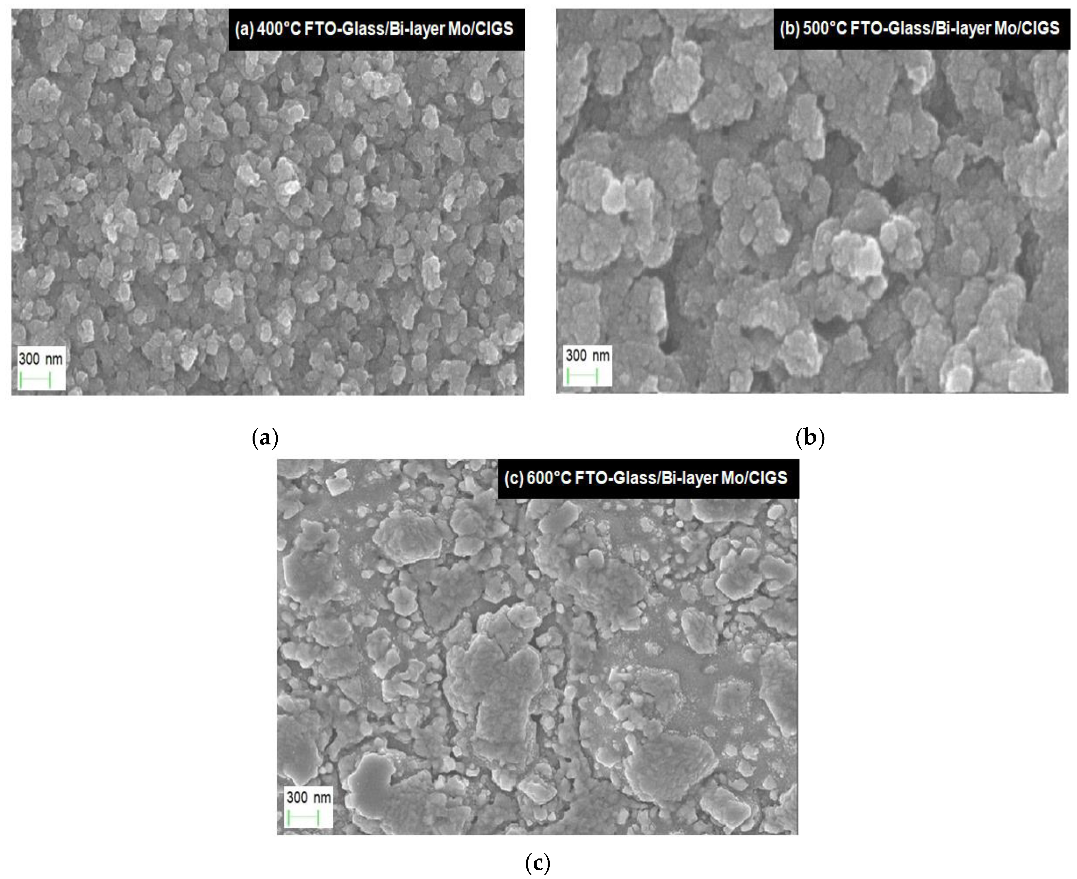
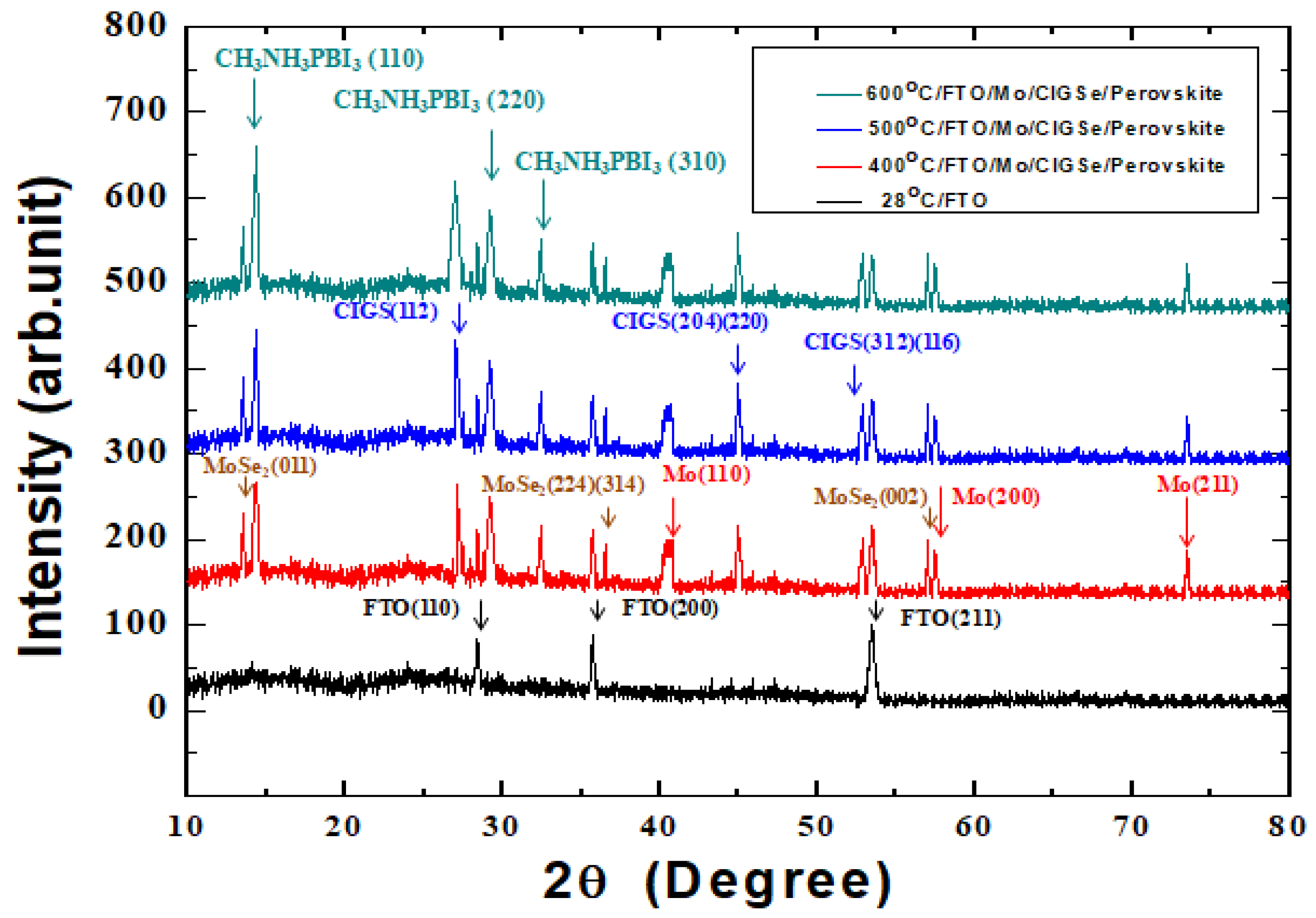
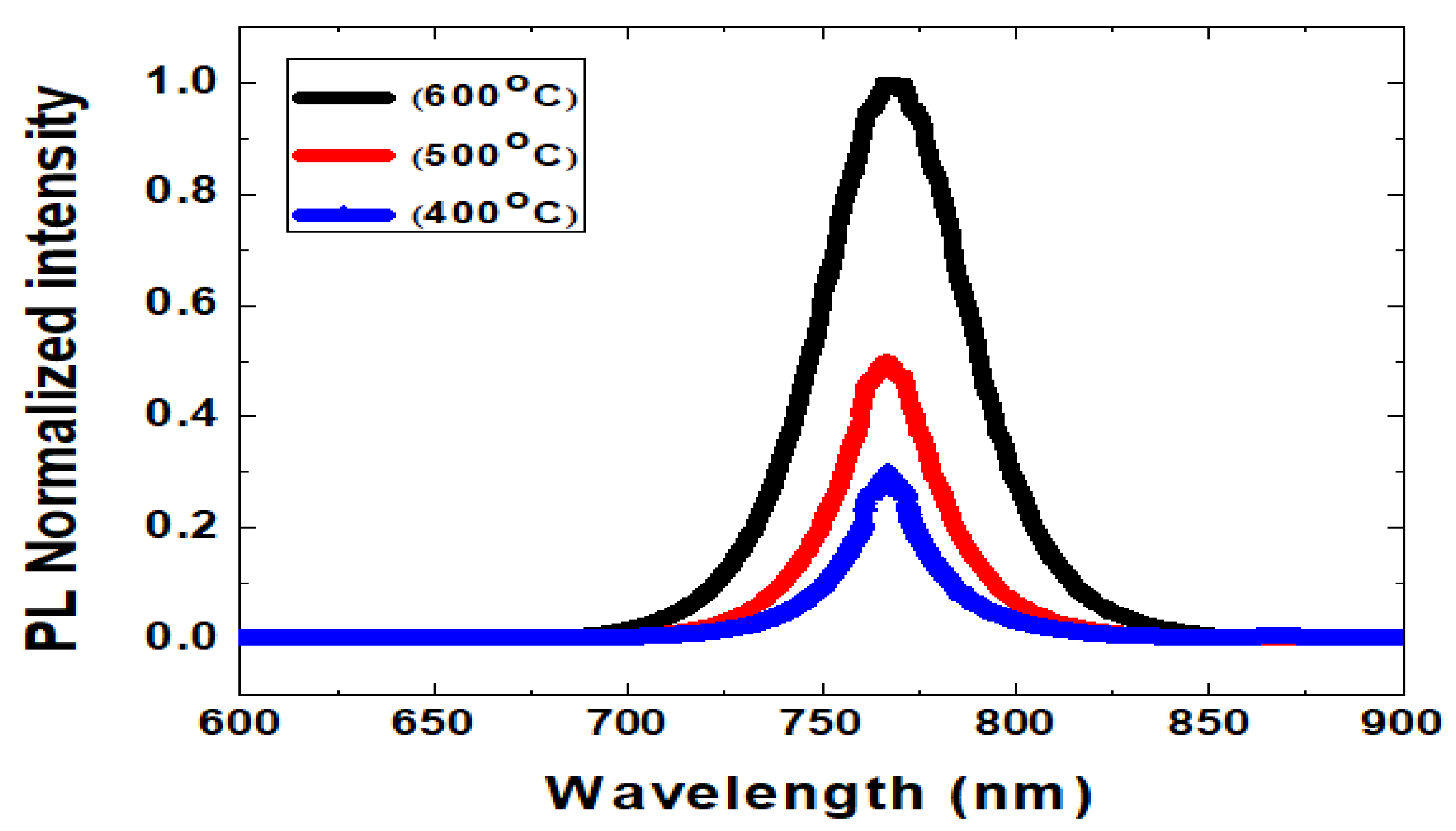
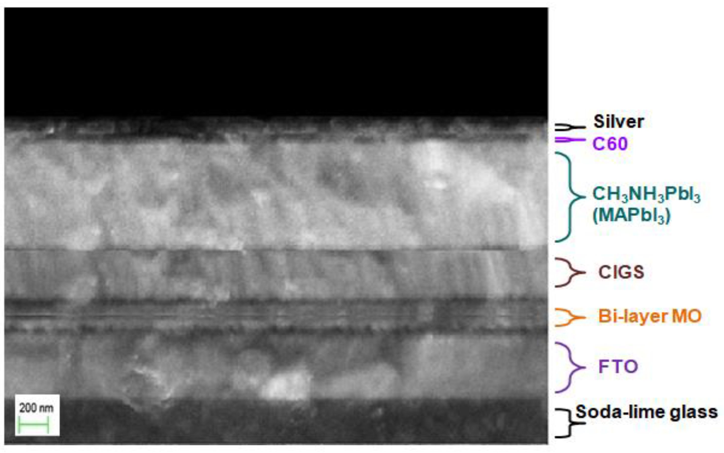
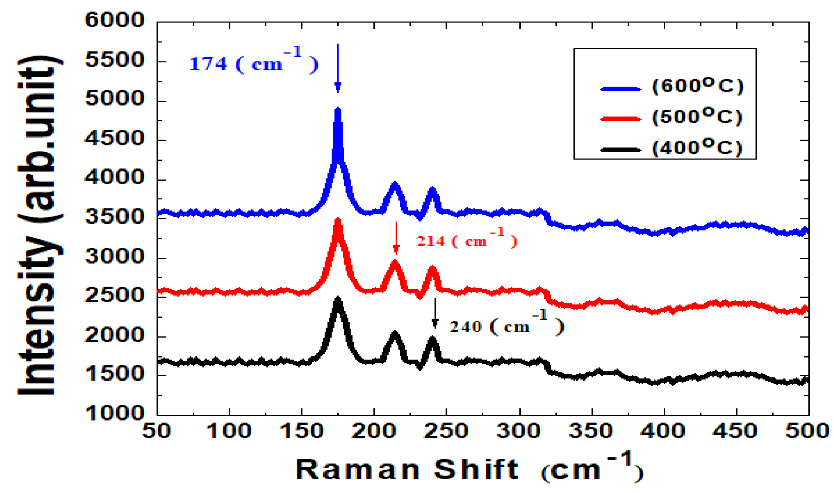
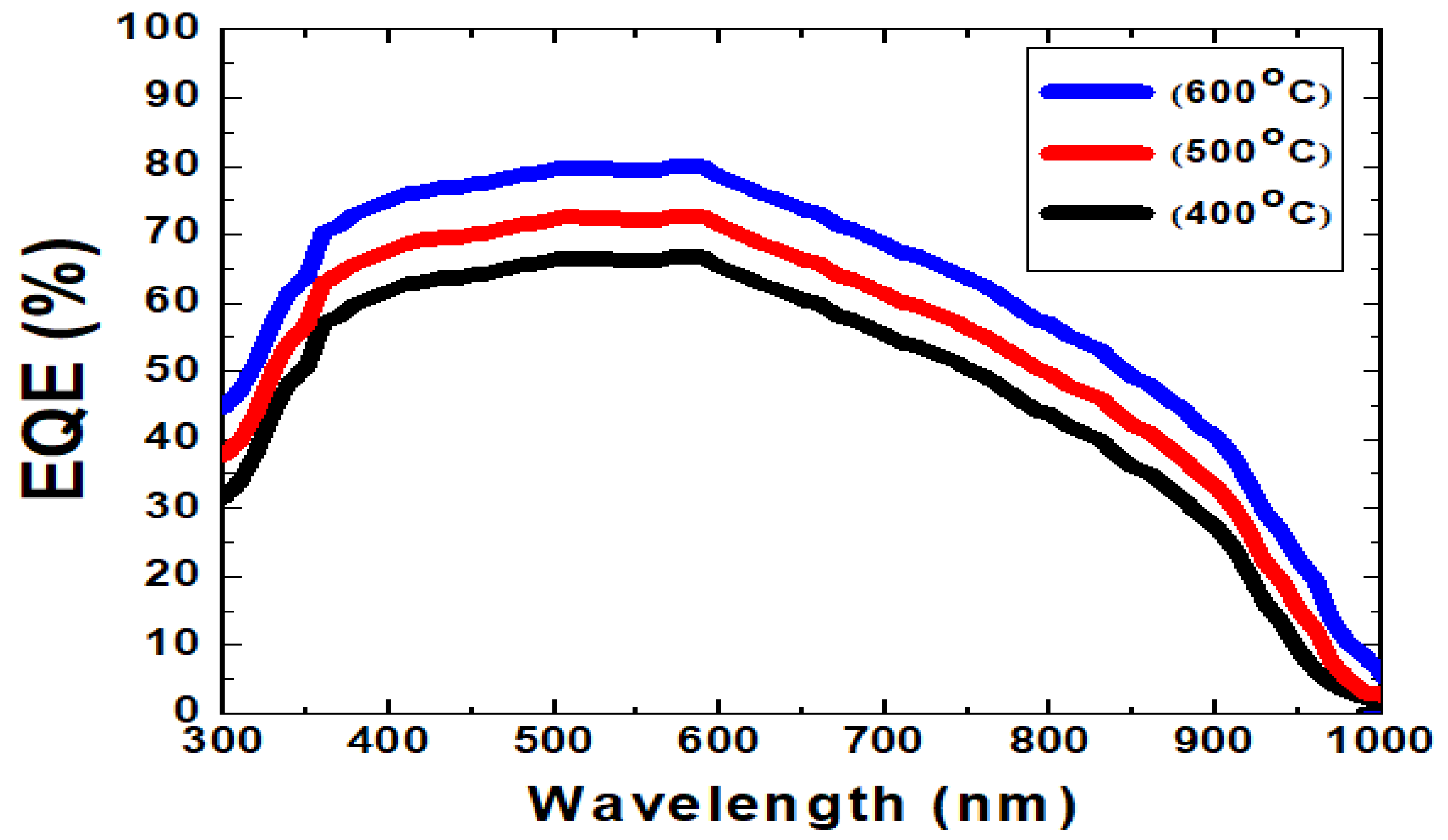
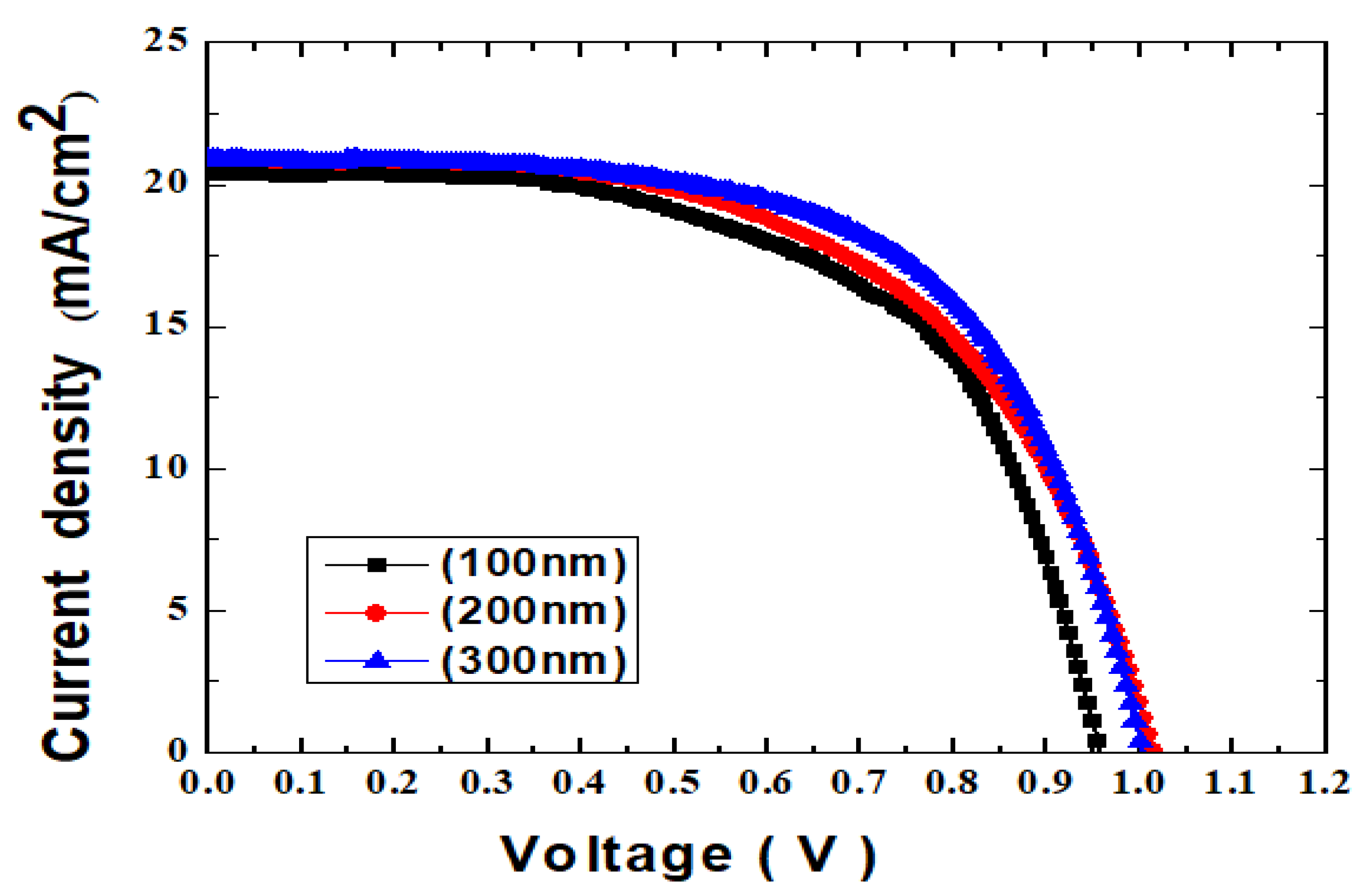
3. Results and Discussion

The morphology of the CuIn1−xGaxSe2 HTM film was investigated by SEM. Figure 2 showsthe top-view SEM morphology ofthe CuIn1−xGaxSe2 HTM films following thermal annealing at various temperatures. The as-formed CuIn1−xGaxSe2 HTM films exhibited full surface coverage and were composed of crystal grains ranging from tens of nm to one μm in size. It has also been evidenced that the nano-crystal grain size increased following the higher annealing temperature. A densely crystallized CuIn1−xGaxSe2 HTM film could be acquired after sintering at the annealing temperature. However, the CuIn1−xGaxSe2 HTM film surface appearance at 400 °C, in Figure 2a, exhibited relatively smaller crystal grains from tens to 300 nm, also involving more pinholes. This defect phenomenon could facilitate incomplete bonding between the multilayer films. Figure 2b showsthe CuIn1−xGaxSe2 HTM film surface appearance from 500 °C annealing with crystallization from tens to 600 nm in grain size, involving fewer pinholes at the same resolution. Figure 2c shows the CuIn1−xGaxSe2 HTM film surface annealed at 600 °C. It exhibited crystals from tens nm to 1 μm in grain size, with scarce pinholes at the same resolution. The lower annealing temperature, on this occasion, led to a film surface involved in more defects or pinholes.
Figure 3 displays the X-ray diffraction spectra of the multi-layer structures. The MAPbI3 film’s nano-crystals exhibit one main crystal plane (110) corresponding to the diffraction peak at ∼14.3°, indicating a strong preferential orientation in the growth direction. The other MAPbI3 film’s crystal plane (220) corresponds to the diffraction peak at ∼29.2°, and crystal plane (310) corresponds to the diffraction peak at ∼32.4°. On the other hand, the CuIn1−xGaxSe2 HTM film nano-crystals exhibit one main crystal plane (112) diffraction peak at ∼26.8°, indicating a strong preferential orientation in the growth direction. It also shows crystal planes (204) (220) diffraction peak at ∼44.9°, and crystal planes (312) (316) diffraction peak at ∼53.0°. The bi-layer Mo film’s nano-crystals exhibit one main crystal plane (110) diffraction peak at ∼40.5°. Other bi-layer Mo film nano-crystals include a crystal plane (200) diffraction peak at ∼58.6° and a crystal plane (211) diffraction peak at ∼73.5°. Additionally, the MoSe2 film nano-crystals exhibit one main crystal plane (011) diffraction peak at ∼13.5°, and crystal planes (224) (314) diffraction peak at ∼36.5°, and crystal plane (002) diffraction peak at ∼57°. The crystallization of MAPbI3 active absorber layer was preceded by the ascension annealing temperature of the CuIn1−xGaxSe2 HTM film. The function of the CuIn1−xGaxSe2 HTM film was a hole-transporting layer and the function of MAPbI3was as an active photovoltaic layer. In addition, the CuIn1−xGaxSe2 HTM film and the MAPbI3 film could be sintered together. Furthermore, the MAPbI3 and CuIn1−xGaxSe2 HTM films’ energy band gapscan be complementary for trapping light simultaneously. As a result, it is composed of pairs of an excited electron and an associated electron-hole for recombination. Subsequently, it can escalate the photon-electron power-conversion efficiency and the associated optical-current for the multilayer structure cells.
Figure 4 shows the photoluminescence (PL) spectra of the MAPbI3/CIGSe/bi-layer Mo/FTO glass following thermal annealing at the various temperatures. One main peak of the PL spectrum wavelength at ∼767 nm is observed. The PL spectrum is light emission from any form of matter after the absorption of photons or electromagnetic radiation. The intensity is associated with the lifetime of the injected electrons and holes that were combined to form excitons in the solar cells. The excitons revealed mobile concentration energy formation by an excited electron and an associated electron-hole. As the excitons intensified during the examination, the number of excitons was enhanced and the electron/electron-hole recombined with each other. As the annealing temperature was increased from 400 to 600 °C, the PL intensity of the MAPbI3 film deposited on the CuIn1−xGaxSe2 HTM film was enhanced. The MAPbI3/CuIn1−xGaxSe2 HTM nano-crystals grown by annealing resulted in ohmic-contact construction and low contact resistance of the CuIn1−xGaxSe2 HTM film with bi-layer Mo film. The CuIn1−xGaxSe2 HTM film was conceived to havegood contact with the active MAPbI3 absorbing layer in the solar cells to improve device stability.
Figure 5 shows the SEM cross-sectional view of the MAPbI3 on CIGSe HTM/bi-layer Mo/FTO glass multi-layer structure, with annealing at 600 °C. The solar cells have been composed of a relatively smooth CIGSe surface, involving few pinholes. Nevertheless, a complete solar cell multi-layer structure of Ag/C60/MAPbI3/CIGSe/Mo/FTO was clearly revealed with a densely packed columnar architecture. Hereafter, Figure 6 shows a Tauc plot for measuring the energy band gap (Eg) at 1.25 eV for the CuIn1−xGaxSe2 HTM grown on a bi-layer Mo/FTO glass-substrate. The band-gap was obtained by extrapolating the linear portion of (αhν)2 vs. graph, where α, h and ν represent the absorption, Planck constant and radiation frequency [65,66]. The energy band gap is required to elevate a valence electron bound to an atom to become a conduction electron and a hole, which can be free to move as charge carriers to conduct an electrical current.
Figure 7 shows the plotted current-density voltage (J–V) curves of MAPbI3 perovskite solar cells with the ultra-thin CuIn1−xGaxSe2HTM nano-structures on bi-layer Mo/FTO glass substrates. The various HTM thicknesses, all at an annealing temperature of 600 °C, were compared here under 100 mW/cm2 illumination (AM 1.5G). At least six cell samples of each type have been fabricated, with the performance deviation ~5%. Additionally, Table 1 summarizes the characteristic parameters of the novel solar cells at the various HTM thicknesses using a 600 °C annealing temperature. The solar cells’ open-circuit voltage could be increased from 0.96 to 1.02 V, with the CuIn1−xGaxSe2 HTM film from 100 to 300 nm. The short-circuit current value also increased from 20.4 to 20.9 mA/cm2. The device fill factor values were slightly diminished from 67.4% to 65.6%. The photovoltaic device PCE ranged from 13.2% to 14.2%. In addition, the device series-resistance was decreased from 16.9 to 15.8 Ω. The output power Pmax effect values increased from 1.32 mW to 1.42 mW.
Furthermore, the fill factor has been defined as the ratio of the output power Pmax to the device open-circuit voltage and short-circuit current at the maximum electric power output. This is the maximum power of the rectangle in the current-voltage characteristic curve. In accordance with the current-density voltage curve and the PCE value, it has been suggested that the optimal thickness of the CuIn1−xGaxSe2 hole-transporting film layer is at ~200 nm. This sample exhibited a slightly higher open-circuit voltage along with the lowest device series-resistance. In this study, it has been desired to develop ultra-thin HTM layers for solar cell applications. The CIGS film quality has been improved and the HTM layer thickness was decreased. In fact, the 300 nm sample also exhibited a reasonably good PSC performance. On the other hand, when the CIGS layer was tried at a thickness below 100 nm (such as 30–50 nm, not shown in this report), not only was the PSC performance was degraded but also the deviation increased appreciably.
An ultra-thin CuIn1−xGaxSe2HTM (<400 nm) has been deposited between the MAPbI3 active absorber material and the bi-layer Mo metal-electrode to promote carrier transport, leading to an improved device witha goodohmic-contact. Additionally, innovative structures of bi-layer Mo films were deposited onto FTO/glass substrates. Eventually, Figure 8 shows the ultra-thin CuIn1−xGaxSe2 hole-transporting material detailed investigation on the compositional dependence of the Raman spectra, grown on a bi-layer Mo/FTO glass substrate. In this work, the CuIn1−xGaxSe2 HTM film exhibited dominant spectra with an intense Raman scattering peak at 174 cm−1, corresponding to the optical phonon mode that was characteristic of the chalcopyrite nano-crystals and nano-structures. The Raman intensities at 174 cm−1, 214 cm−1 and 240 cm−1 were slightly increased while increasing the annealing temperature. The CuIn1−xGaxSe2 HTM crystal orientation could be found from the polarization of Raman-scattered light with respect to the laser light if the crystal structure’s point group was known.
Figure 9 shows the device measured external quantum efficiency (EQE) curve results due to optical modification with CuIn1−xGaxSe2 hole-transporting material. The spectra included experimentally measured EQE curves with an entire major spectral feature, which reproduced in both wavelength and amplitude. Notably, the EQE results with ultra-thin CuIn1−xGaxSe2 HTM exhibited the maximum EQE of ~78% for the 600 °C-annealed sample, observed between 500 nm and 600 nm. It was attributed to the combined effects of Fabry-Perot resonances and efficient coupling into the waveguide modes of the absorber layer [67,68]. Planar CuIn1−xGaxSe2 solar cells contained translational invariant and an electric field distribution by resonances.

4. Conclusions

In summary, sputtering-processed CuIn1−xGaxSe2 nano-crystals have been successfully applied as a novel Cu-based inorganic HTM for solar cells. The PCE of the CuIn1−xGaxSe2 HTM-based photovoltaic device has been reached at 14.2%, which is quite encouraging for conventional solar cells with Cu-based chalcopyrite semiconductor HTMs. In addition, the CuIn1−xGaxSe2 HTM/MAPbI3 perovskite layers that involved MoSe2 exhibited a good ohmic-contact. This work provided a promising candidate of Cu-based inorganic HTM for stable perovskite solar cells, and dedicated investigation about characteristics of silver/C60/CH3NH3PbI3/CIGSe/bi-layer Mo/FTO multilayer of nano-structured devices. The SEM morphology observation on CuIn1−xGaxSe2 HTM film following thermal annealing at 400, 500, and 600 °C revealed crystal grains ranging from tens nm to one μm in size. The pinhole and defect density wasalso decreased with the increasing annealing temperature. The experimental results of MAPbI3 perovskite solar cells with the optimal 200 nm CuIn1−xGaxSe2 HTM nano-structures that were annealed at 600 °C showed a better PCE of 14.2%. This device exhibited that the VOC, JSC, FF, PCE, Rs, and Pmax were 1.02 V, 20.9 mA/cm2, 66.6%, 14.2%, 15.8 Ω, and 1.42 mW, respectively.

Author Contributions

Investigation, L.-B.C., C.-C.T., G.W., W.-S.F. and M.-J.J.; methodology, L.-C.C. and K.-L.L.; resources, E.P., L.J. and K.G.; writing—original draft preparation, C.-C.T.; writing—review and editing, G.W.

Funding

This work was supported in part by the Ministry of Science and Technology under research grants MOST105-2221-E182-059-MY3, MOST105-2221-B182-059-MY3, and MOST106-2221-E182-060. The APC was funded by CGMH/CGU under CMRPD3G0062 and BMRP246.

Conflicts of Interest

The authors declare no conflict of interest.

References

  1. Correa-Baena, J.B.; Abate, A.; Saliba, M.; Tress, W.; Jacobsson, T.J.; Gratzelc, M.; Hagfeldt, A. The rapid evolution of highly efficient perovskite solar cells. Energy Environ. Sci. 2017, 10, 710–727. [Google Scholar] [CrossRef]
  2. Dubey, A.; Adhikari, N.; Mabrouk, S.; Wu, F.; Chen, K.; Yang, S.; Qiao, Q. A strategic review on processing routes towards highly efficient perovskite solar cells. J. Mater. Chem. A 2018, 6, 2406–2431. [Google Scholar] [CrossRef]
  3. Meng, L.; You, J.; Guo, T.; Yang, Y. Recent advances in the inverted planar structure of perovskite solar cells. Acc. Chem. Res. 2016, 49, 155–165. [Google Scholar] [CrossRef]
  4. Dubey, A.; Adhikari, N.; Venkatesan, S.; Gu, S.; Khatiwada, D.; Wang, Q.; Mohammad, L.; Kumar, M.; Qiao, Q. Solution processed pristine PDPP3T polymer as hole-transport layer for efficient perovskite solar cells with slower degradation. Solar Energy Mater. Solar Cells 2016, 145, 193–199. [Google Scholar] [CrossRef]
  5. Wu, W.; Chen, D.; Caruso, R.A.; Cheng, Y. Recent progress in hybrid perovskite solar cells based on n-type materials. J. Mater. Chem. A 2017, 5, 10092–10109. [Google Scholar] [CrossRef]
  6. Ahmadian-Yazdi, M.; Habibi, M.; Esiamian, M. Excitation of wet perovskite films by ultrasonic vibration improves the device performance. Appl. Sci. 2018, 8, 308. [Google Scholar] [CrossRef]
  7. Zuo, C.; Bolink, H.J.; Han, H.; Huang, J.; Cahen, D.; Ding, L. Advances in perovskite solar cells. Adv. Sci. 2016, 3, 1500324. [Google Scholar] [CrossRef]
  8. Wang, R.; Wu, X.; Xu, K.; Zhou, W.; Shang, Y.; Tang, H.; Chen, H.; Ning, Z. Highly efficient inverted structural quantum dot solar cells. Adv. Mater. 2018, 30, 1704882. [Google Scholar] [CrossRef]
  9. Pierini, F.; Lanzi, M.; Nakielski, P.; Pawlowska, S.; Urbanek, O.; Zembrzycki, K.; Kowalewski, T.A. Single-material organic solar cells based on electro spun fullerene-grafted polythiophene nanofibers. Macromolecules 2017, 50, 4972–4981. [Google Scholar] [CrossRef]
  10. Mitzi, D.B.; Chondroudis, K.; Kagan., C.R. Design, structure, and optical properties of organic inorganic perovskites containing an oligothiophenechromophor. Prog. Inorg. Chem. 1999, 38, 6246–6256. [Google Scholar] [CrossRef]
  11. Mitzi, D.B. Synthesis, structure, properties of organic-inorganic perovskites and related materials. Prog. Inorg. Chem. 2007, 48, 1–121. [Google Scholar]
  12. Jeon, N.J.; Noh, J.H.; Yang, W.S.; Kim, Y.C.; Ryu, S.; Seo, J.; Seok, S.I. Compositional engineering of perovskite materials for high-performance solar cells. Nature 2015, 517, 476. [Google Scholar] [CrossRef] [PubMed]
  13. Liu, M.; Johnston, M.B.; Snaith, H.J. Efficient planar heterojunction perovskite solar cells by vapour deposition. Nature 2013, 501, 396. [Google Scholar] [CrossRef] [PubMed]
  14. Im, J.H.; Jang, I.H.; Pellet, N.; Gratzel, M.; Park, N. Growth of CH3NH3PbI3 cuboids with controlled size for high-efficiency perovskite solar cells. Nat. Nanotechnol. 2014, 9, 927–932. [Google Scholar] [CrossRef] [PubMed]
  15. Yang, W.S.; Noh, J.H.; Jeon, N.J.; Kim, Y.C.; Ryu, S.; Seo, J.; Seok, S.I. High-performance photovoltaic perovskite layers fabricated through intramolecular exchange. Science 2015, 348, 1234–1237. [Google Scholar] [CrossRef] [PubMed]
  16. Sani, F.; Shafie, S.; Lim, H.N.; Musa, A.O. Advancement on lead-free organic-inorganic halide perovskite solar cells: A review. Materials 2018, 11, 1008. [Google Scholar] [CrossRef]
  17. Xing, G.; Mathews, N.; Sun, S.; Lim, S.S.; Lam, Y.M.; Gratzel, M.; Mhaisalkar, S.; Sum, T.C. Long-range balanced electron- and hole-transport lengths in organic-inorganic CH3NH3PbI3. Science 2013, 342, 344–347. [Google Scholar] [CrossRef]
  18. Stranks, S.D.; Eperon, G.E.; Grancini, G.; Menelaou, C.; Alcocer, M.J.; Leijtens, T.; Herz, L.M.; Petrozza, A.; Snaith, H.J. Electron-hole diffusion lengths exceeding 1 micrometer in an organometaltrihalide perovskite absorber. Science 2013, 342, 341–344. [Google Scholar] [CrossRef]
  19. Kojima, A.; Teshima, K.; Shirai, Y.; Miyasaka, T. Organometal halide perovskites as visible-light sensitizers for photovoltaic cells. J. Am. Chem. Soc. 2009, 131, 6050–6051. [Google Scholar] [CrossRef]
  20. Kim, H.S.; Lee, C.R.; Im, J.H.; Lee, K.B.; Moehl, T.; Marchioro, A.; Moon, S.J.; Humphry-Baker, R.; Yum, J.H.; Moser, J.E.; et al. Lead iodide perovskite sensitized all-solid-state submicron thin film mesoscopic solar cell with efficiency exceeding 9%. Sci. Rep. 2012, 2, 591. [Google Scholar] [CrossRef]
  21. Jeng, J.Y.; Chiang, Y.F.; Lee, M.H.; Peng, S.R.; Guo, T.F.; Chen, P.; Wen, T.C. CH3NH3PbI3 perovskite/fullerene planar-heterojunction hybrid solar cells. Adv. Mater. 2013, 25, 3727–3732. [Google Scholar] [CrossRef] [PubMed]
  22. Chen, L.M.; Hong, Z.; Li, G.; Yang, Y. Recent progress in polymer solar cells: Manipulation of polymer: Fullerene morphology and the formation of efficient inverted polymer solar cells. Adv. Mater. 2009, 21, 1434–1449. [Google Scholar] [CrossRef]
  23. Choi, H.; Mai, C.; Kim, H.; Jeong, J.; Song, S.; Bazan, G.C.; Kim, J.Y.; Heeger, A.J. Conjugated polyelectrolyte hole transport layer for inverted-type perovskite solar cells. Nat. Commun. 2015, 6, 7348. [Google Scholar] [CrossRef] [PubMed] [Green Version]
  24. Li, Z.; Klein, T.R.; Kim, D.H.; Yang, M.; Berry, J.J.; van Hest, M.F.; Zhu, K. Scalable fabrication of perovskite solar cells. Nat. Rev. Mater. 2018, 3, 18017. [Google Scholar] [CrossRef]
  25. Christians, J.A.; Schulz, P.; Tinkham, J.S.; Schloemer, T.H.; Harvey, S.P.; Tremolet de Villers, B.J.; Sellinger, A.; Berry, J.J.; Luther, J.M. Tailored interfaces of unencapsulated perovskite solar cells for >1000 hour operational stability. Nat. Energy 2018, 3, 68–74. [Google Scholar] [CrossRef]
  26. Snaith, H.J.; Hacke, P. Enabling reliability assessments of pre-commercial perovskite photovoltaics with lessons learned from industrial standards. Nat. Energy 2018, 3, 459–465. [Google Scholar] [CrossRef]
  27. Habisreutinger, S.N.; McMeekin, D.P.; Snaith, H.J.; Nicholas, R.J. Research update: Strategies for improving the stability of perovskite solar cells. APL Mater. 2016, 4, 091503. [Google Scholar] [CrossRef]
  28. Kim, J.; Yang, J.; Yu, J.H.; Baek, W.; Lee, C.; Son, H.J.; Hyeon, T.; Ko, M.J. Highly efficient copper–indium–selenide quantum dot solar cells: Suppression of carrier recombination by controlled ZnS overlayers. ACS Nano 2015, 9, 11286–11295. [Google Scholar] [CrossRef]
  29. Lian, L.; Xia, Y.; Zhang, C.; Xu, B.; Yang, L.; Liu, H.; Zhang, D.; Wang, K.; Gao, J.; Zhang, J. In situ tuning the reactivity of selenium precursor to synthesize wide range size, ultra large-scale, and ultrastable PbSe quantum dots. Chem. Mater. 2018, 30, 982–989. [Google Scholar] [CrossRef]
  30. Wen, X.; Chen, C.; Lu, S.; Li, K.; Kondrotas, R.; Zhao, Y.; Chen, W.; Gao, L.; Wang, C.; Zhang, J.; et al. Vapor transport deposition of antimony selenide thin film solar cells with 7.6% efficiency. Nat. Commun. 2018, 9, 2179. [Google Scholar] [CrossRef]
  31. Sapkota, Y.R.; Mazumdar, D. Bulk transport properties of bismuth selenide thin films grown by magnetron sputtering approaching the two-dimensional limit. J. Appl. Phys. 2018, 124, 105306. [Google Scholar] [CrossRef]
  32. Wei, S.H.; Zunger, A. Band offsets and optical bowings of chalcopyrites and Zn-based II-VI alloys. J. Appl. Phys. 1995, 78, 3846–3856. [Google Scholar] [CrossRef]
  33. Van Lare, C.; Yin, G.; Polman, A.; Schmid, M. Light coupling and trapping in ultrathin Cu(In,Ga)Se2 solar cells using dielectric scattering patterns. ACS Nano 2015, 9, 9603–9613. [Google Scholar] [CrossRef] [PubMed]
  34. Han, A.; Zhang, Y.; Song, W.; Li, B.; Liu, W.; Sun, Y. Structure, morphology and properties of thinned Cu(In, Ga)Se2 films and solar cells. Semicond. Sci. Technol. 2012, 27, 3. [Google Scholar] [CrossRef]
  35. Saifullah, M.; Ahn, S.; Gwak, J.; Ahn, S.; Kim, K.; Cho, J.; Park, J.H.; Eo, Y.J.; Cho, A.; Yoo, J.U.; et al. Development of semitransparent CIGS thin-film solar cells modified with a sulfurized-AgGa layer for building applications. J. Mater. Chem. A 2016, 4, 10542–10551. [Google Scholar] [CrossRef]
  36. Wu, G.M.; Lin, H.H.; Lu, H.C. Work function and valance band structure of tin-doped indium oxide thin film for OLED. Vacuum 2008, 82, 1371. [Google Scholar] [CrossRef]
  37. Yin, G.; Brackmann, V.; Hoffmann, V.; Schmid, M. Enhanced performance of ultra-thin Cu(In,Ga)Se2 solar cells deposited at low process temperature. Solar Energy Mater. Solar Cells 2005, 132, 142–147. [Google Scholar] [CrossRef]
  38. Martin, F.; Muralt, P.; Dubois, M.A. Process optimization for the sputter deposition of molybdenum thin films as electrode for AlN thin films. J. Vacuum Sci. Technol. A 2006, 24, 946–952. [Google Scholar] [CrossRef]
  39. Li, Z.H.; Cho, E.S.; Kwon, S.J. Molybdenum thin film deposited by in-line DC magnetron sputtering as a back contact for Cu(In,Ga)Se2 solar cells. Appl. Surf. Sci. 2011, 257, 9682–9688. [Google Scholar] [CrossRef]
  40. Ma, X.; Liu, D.; Yang, L.; Zuo, S.; Zhou, M. Molybdenum (Mo) back contacts for CIGS solar cell. Proc. of SPIE 2013, 9068, 906814. [Google Scholar] [CrossRef]
  41. Jaegaermann, W.; Loher, T.; Pettenkofer, C. Surface properties of chalcopyrite semiconductors. Cryst. Res. Cryst. Technol. 1996, 31, 273. [Google Scholar]
  42. Alvarez-Garcia, J.; Perez-Rodriguez, A.; Romano-Rodriguez, A.; Morante, J.R.; Calvo-Barrio, L.; Scheer, R.; Klenk, R. Microstructure and secondary phases in co-evaporated CuInS2 films: Dependence on growth temperature and chemical composition. J. Vac. Sci. Technol. A 2001, 19, 232–239. [Google Scholar] [CrossRef]
  43. Wada, T.; Kohara, N.; Nishiwaki, S.; Negami, T. Characterization of the Cu (In, Ga) Se2/Mo interface in CIGS solar cells. Thin Solid Films 2001, 387, 118–122. [Google Scholar] [CrossRef]
  44. Schmid, D.; Ruckh, M.; Schock, H.W. A comprehensive characterization of the interfaces in Mo/ CIS/CdS/ZnOsolarcell structures. Solar Energy Mater. Solar Cells 1996, 41, 281–294. [Google Scholar] [CrossRef]
  45. Klinkert, T.; Patriarche, G.; Theys, B.; Theys, B. New insights into the Mo/Cu(In,Ga)Se2 interface in thin film solar cells: Formation and properties of the MoSe2 interfacial layer. J. Chem. Phys. 2016, 145, 154702. [Google Scholar] [CrossRef] [PubMed]
  46. Wada, T.; Kohara, N.; Negami, T.; Nishitani, M. Chemical and structural characterization of Cu(In, Ga)Se2/Mo interface in Cu(In, Ga)Se2 solar cells. Jpn. J. Appl. Phys. 1996, 35, L1253–L1256. [Google Scholar] [CrossRef]
  47. Duchatelet, A.; Savidand, G.; Vannier, R.N.; Lincot, D. Optimization of MoSe2 formation for Cu(In,Ga)Se2-based solar cells by using thin superficial molybdenum oxide barrier layers. Thin Solid Films 2013, 545, 94–99. [Google Scholar] [CrossRef]
  48. Zhang, X.; Kobayashi, M.; Yamada, A. Comparison of Ag(In,Ga)Se2/Mo and Cu(In,Ga)Se2/Mo interfaces in solar cells. ACS Appl. Mater. Interfaces 2017, 9, 16215–16220. [Google Scholar] [CrossRef]
  49. Schmid, M.; Klenk, R.; Lux-Steiner, M.C.; Topic, M. Modeling plasmonic scattering combined with thin-film optics. Nanotechnology 2011, 22, 025204. [Google Scholar] [CrossRef]
  50. Schmid, M.; Klaer, J.; Klenk, R.; Topic, M.J. Stability of plasmonicmetalnanoparticles integrated in the back contact of ultra-thin Cu(In,Ga)S2 solar cells. Thin Solid Films 2013, 527, 308–313. [Google Scholar] [CrossRef]
  51. Amin, N.; Chelvanathan, P.; Hossain, M.I.; Sopian, K. Numerical modelling of ultra thin Cu(In,Ga)Se2 solar cells. Energy Procedia 2011, 15, 291–298. [Google Scholar] [CrossRef]
  52. Gloeckler, M.; Sites, J.R. Potential of submicrometer thickness Cu(In,Ga)Se2 solar cells. J. Appl. Phys. 2005, 98, 103703. [Google Scholar] [CrossRef]
  53. Xu, L.; Deng, L.; Cao, J.; Wang, X.; Chen, W.; Jiang, Z. Solution-processed Cu(In,Ga)(S,Se)2 nanocrystal as inorganic hole-transporting material for efficient and stable perovskite solar cells. Nanoscale Res. Lett. 2017, 12, 159. [Google Scholar] [CrossRef] [PubMed]
  54. Heo, J.H.; Im, S.H.; Noh, J.H.; Mandal, T.N.; Lim, C.S.; Chang, J.A.; Lee, Y.H.; Sarkar, A.; Nazeeruddin, M.K. Efficient inorganic-organic hybrid heterojunction solar cells containing perovskite compound and polymeric hole conductors. Nat. Photonic 2013, 7, 486–491. [Google Scholar] [CrossRef]
  55. Noh, J.H.; Im, S.H.; Heo, J.H.; Mandal, T.N.; Seok, S.I. Chemical management for colorful, efficient, and stable inorganic-organic hybrid nanostructured solar cells. Nano. Lett. 2013, 13, 1764–1769. [Google Scholar] [CrossRef] [PubMed]
  56. Niu, G.; Li, W.; Meng, F.; Wang, L.; Dong, H.; Qiu, Y. Study on the stability of CH3NH3PbI3 (MAPbI3) films and the effect of post-modification by aluminum oxide in all-solid-state hybrid solar cells. J. Mater. Chem. A 2014, 2, 705–710. [Google Scholar] [CrossRef]
  57. Christians, J.A.; Fung, R.C.; Kamat, P.V. An inorganic hole conductor for organo-lead halide perovskite solar cells: Improved hole conductivity with copper iodide. J. Am. Chem. Soc. 2013, 136, 758–764. [Google Scholar] [CrossRef]
  58. Chen, W.Y.; Deng, L.L.; Dai, S.M.; Wang, X.; Tian, C.B.; Zhan, X.X.; Xie, S.Y.; Huang, R.B.; Zheng, L.S. Low-cost solution-processed copper iodide as an alternative to PEDOT:PSS hole transport layer for efficient and stable inverted planar heterojunction perovskite solar cells. J. Mater. Chem. A 2015, 3, 19353–19359. [Google Scholar] [CrossRef]
  59. Li, Y.; Zhu, J.; Huang, Y.; Wei, J.; Liu, F.; Shao, Z.; Hu, L.; Chen, S.; Yang, S.; Tang, J.; et al. Efficient inorganic solid solar cells composed of perovskite and PbS quantum dots. Nanoscale 2015, 7, 9902–9907. [Google Scholar] [CrossRef]
  60. Kim, J.H.; Liang, P.W.; Williams, S.T.; Cho, N.; Chueh, C.C.; Glaz, M.S.; Ginger, D.S.; Jen, A.K. High-performance and environmentally stable planar heterojunction perovskite solar cells based on a solution-processed copper-doped nickel oxide hole-transporting layer. Adv. Mater. 2015, 27, 695–701. [Google Scholar] [CrossRef]
  61. Lu, M.; Zhu, J.; Huang, Y.; Li, Y.; Shao, Z.; Xu, Y.; Dai, S. Colloidal CuInS2 quantum dots as inorganic hole-transporting material in perovskite solar cells. ACS Appl. Mater. Interfaces 2015, 7, 17482–17488. [Google Scholar]
  62. Chen, J.; Park, N. Inorganic hole transporting materials for stable and high efficiency perovskite solar cells. J. Phys. Chem. C 2018, 8, 01177. [Google Scholar] [CrossRef]
  63. Yoshida, K.; Oku, T.; Suzuki, A.; Akiyama, T.; Yamasaki, Y. Fabrication and characterization of phthalocyanine/C60 solar cells with inverted structure. Adv. Chem. Eng. Sci. 2012, 2, 461–464. [Google Scholar] [CrossRef]
  64. Kim, D.Y.; So, F.; Gao, Y. Aluminum phthalocyanine chloride/C60 organic photovoltaic cells with high open-circuit voltages. Solar Energy Mater. Solar Cells 2009, 93, 1688–1691. [Google Scholar] [CrossRef]
  65. Bakr, N.A.; Khodair, Z.T.; Mahdi, H.I. Influence of thiourea concentration on some physical properties of chemically sprayed Cu2ZnSnS4 thin films. Intl. J. Mater. Sci. Appl. 2016, 5, 261–270. [Google Scholar]
  66. Sahoo, A.K.; Wu, G.M. Effects of argon flow rate on electrical properties of amorphous indium gallium zinc oxide thin-film transistors. Thin Solid Films 2016, 605, 129–135. [Google Scholar] [CrossRef]
  67. Yin, G.; Knight, M.W.; van Lare, M.; Magdalena, M.; Garcia, S.; Polman, A.; Schmid, M. Optoelectronic enhancement of ultrathin CuIn1–xGaxSe2solar cells by nanophotonic contacts. Adv. Opt. Mater. 2017, 5, 1600637. [Google Scholar] [CrossRef]
  68. Jheng, B.T.; Liu, P.; Wu, M. Efficiency enhancement of non-selenized Cu(In,Ga)Se2 solar cells employing scalable low-cost antireflective coating. Nanoscale Res. Lett. 2014, 9, 331. [Google Scholar] [CrossRef]
Figure 1. A schematic diagram of the perovskite solar cell with ultra-thin CuIn1−xGaxSe2 hole-transporting material layer.
Applsci 09 00719 g001
Figure 2. Top-view scanning electron microscope images of the ultra-thin CuIn1−xGaxSe2 hole-transporting material layer following thermal annealing at the various temperatures (a) 400 °C, (b) 500 °C, and (c) 600 °C.
Applsci 09 00719 g002
Figure 3. The X-ray diffraction pattern results of CH3NH3PbI3 (MAPbI3) perovskite solar cells with CuIn1−xGaxSe2 HTM (hole-transporting material) multi-layer structures.
Applsci 09 00719 g003
Figure 4. PL (photoluminescence) spectra of MAPbI3/CIGSe HTM/bi-layerMo/FTO (fluorine-tin- oxide) glass following various thermal annealing temperatures at 400, 500, and 600 °C.
Applsci 09 00719 g004
Figure 5. The field-emission SEM cross-sectional view of CH3NH3PbI3 (MAPbI3) the perovskite solar cell witha CuIn1−xGaxSe2 HTM/bi-layer Mo/FTO glass substrate. The CuIn1−xGaxSe2HTM layer was annealed at 600 °C.
Applsci 09 00719 g005
Figure 6. Tauc plot for measuring the energy band gap for CuIn1−xGaxSe2 HTM grown on a bi-layer Mo/FTO glass substrate. The red line was used to extrapolate the band-gap.
Applsci 09 00719 g006
Figure 7. J–V curves of MAPbI3 perovskite solar cells with ultra-thin CuIn1−xGaxSe2HTM nano-structures on a bi-layer Mo/FTO glass substrate, using various HTM thicknesses with a 600 °C thermal annealing temperature. Measurement under 100 mW/cm2 illumination (AM 1.5G).
Applsci 09 00719 g007
Figure 8. Compositional dependence of Raman spectra of CuIn1−xGaxSe2 hole-transporting material layer that was grown on a bi-layer Mo/FTO glass substrate.
Applsci 09 00719 g008
Figure 9. The measured results of external quantum efficiency (EQE) spectra based onsilver/C60/MAPbI3/CIGSe/Mo/FTO solar cells.
Applsci 09 00719 g009
Table 1. Characteristic parameters of the novel solar cells at the various HTM thicknesses using a 600 °C thermal annealing temperature.
HTM Thickness (nm)VOC (V)JSC (mA/cm2)FF (%)Eff (%)RS (Ω)Pmax (mW)
1000.9620.467.413.216.91.32
2001.0220.966.614.215.81.42
3001.0020.965.613.716.21.37

