Article

Effects of Bottom Layer Sputtering Pressures and Annealing Temperatures on the Microstructures, Electrical and Optical Properties of Mo Bilayer Films Deposited by RF/DC Magnetron Sputtering

1
School of Physical Engineering, Zhengzhou University, Zhengzhou 450052, China
2
School of Materials science and Engineering, Henan University of Science and Technology, Luoyang 471023, China
*
Author to whom correspondence should be addressed.
Appl. Sci. 2019, 9(7), 1395; https://doi.org/10.3390/app9071395
Submission received: 1 March 2019 / Revised: 17 March 2019 / Accepted: 29 March 2019 / Published: 3 April 2019
(This article belongs to the Special Issue CIGS Thin Films and Solar Cells)

Abstract

:
Most of the molybdenum (Mo) bilayer films are deposited by direct current (DC) magnetron sputtering at the bottom and the top layer (DC/DC). However, the deposition of Mo bilayer film by radio frequency (RF) Mo bottom layer and DC Mo top layer magnetron sputtering has been less studied by researchers. In this paper, the bottom layer of Mo bilayer film was deposited by RF magnetron sputtering to maintain its good adhesion and high reflectance, and the top layer was deposited by DC magnetron sputtering to obtain good conductivity (RF/DC). Generally, the bottom layer sputtering pressure is relatively random, in this paper, the effects of the bottom layer RF sputtering pressures on the microstructures and properties of Mo bilayer films were first studied in detail. Next, in order to further improve their properties, the as-prepared Mo bilayer films at 0.4 Pa bottom layer RF sputtering pressure were annealed at different temperatures and then investigated. Specifically, Mo bilayer films were deposited on soda-lime glass substrates by RF/DC magnetron sputtering at different bottom layer RF sputtering pressures in the range of 0.4–1.2 Pa, the powers of bottom layer RF sputtering and top layer DC sputtering were 120 W and 100 W, respectively. Then, Mo bilayer films, prepared at a bottom layer sputtering pressure of 0.4 Pa and top layer sputtering pressure of 0.3 Pa, were annealed for 30 min at various temperatures in the range of 100–400 °C. The effects of bottom layer sputtering pressures and the annealing temperatures on the microstructures, electrical and optical properties of Mo bilayer films were clarified by X-ray diffraction (XRD), field emission scanning electron microscopy (FE-SEM), atomic-force microscopy (AFM), and ultraviolet (UV)-visible spectra, respectively. It is shown that with decreasing bottom layer sputtering pressure from 1.2 to 0.4 Pa and increasing annealing temperature from 100 to 400 °C, the crystallinity, electrical and optical properties of Mo bilayer films were improved correspondingly. The optimized Mo bilayer film was prepared at the top layer sputtering pressure of 0.3 Pa, the bottom layer sputtering pressure of 0.4 Pa and the annealing temperature of 400 °C. The extremely low resistivity of 0.92 × 10⁻⁵ Ω.cm was obtained. The photo-conversion efficiency of copper indium gallium selenium (CIGS) solar cell with the optimized Mo bilayer film as electrode was up to as high as 13.5%.

1. Introduction

Molybdenum (Mo) thin films have received considerable attention for various applications such as protective coatings, source/drain electrodes, integrated circuits and solar cells, due to their high thermal and chemical stability, high electrical conductivity and resistance to corrosion [1,2,3,4,5]. Magnetron sputtering is the most commonly used method for the preparation of Mo films originating from several advantages such as low cost, easy to adjust the parameters, films can be deposited uniformly on large-sized areas [6]. A large number of studies have shown that the structures and properties of Mo films are related to the preparation process and parameters [7,8,9]. For instance, Akçay et al., [10] investigated the effects of deposition pressures and powers on the structures and photoelectric properties of Mo films prepared by radio frequency (RF) magnetron sputtering. Nwakanma et al., [11] reported the effects of the sputtering powers and sputtering pressures on the Mo films deposited using direct current (DC) magnetron sputtering. The results clearly indicated that the sputtering powers, sputtering pressures and temperatures had significant influences on grain sizes, optical and electrical properties of Mo thin films prepared by either RF or DC magnetron sputtering.
Generally, it is very difficult for Mo thin films to possess low electrical resistivity and good adhesion to the substrate, simultaneously. Specifically, films deposited at lower sputtering pressure have lower electrical resistivity but poor adhesion, whereas those deposited at higher sputtering pressure have better adhesion but higher electrical resistivity. To solve the problem, Scofield et al., [12] designed a Mo bilayer film, which consisted of a bottom layer deposited at higher sputtering pressure for better adhesion and a top layer deposited at lower sputtering pressure for better conductivity. Since then, many researchers have begun to focus on the effects of processing parameters on structures and properties of the Mo bilayer films prepared by RF/RF and/or DC/DC magnetron sputtering. In the work of Huang et al., [13] the Mo bilayer films prepared by DC/DC magnetron sputtering were optimized. The results indicated that the copper indium gallium selenium (CIGS) solar cell had the maximum photo-conversion efficiency of 12.83%. Badgujar et al., [14] investigated the effects of sputtering powers and argon gas flow rates on the properties of Mo bilayer films prepared by DC/DC magnetron sputtering. The results showed that better crystallinity, reflectance and electrical conductivity were obtained at higher sputtering power and lower argon gas flow rate. Zhu et al. [15] studied the properties of Mo bilayer films prepared by RF/RF and DC/DC sputtering modes, demonstrating that a high efficiency of CIGS thin films solar cell was achieved to be 16.2%. However, fewer people focused on the influences of processing parameters on the properties of Mo bilayer films prepared by RF/DC sputtering method. Commonly, Mo films prepared by RF sputtering have better adhesion to the substrate and higher reflectance but lower conductivity than those prepared by DC sputtering under the same sputtering conditions, but the Mo films prepared by DC sputtering have better conductivity [16]. Actually, the reflectance of Mo back electrode is also very important to the Cu(In,Ga)Se2 (CIGS), copper zinc tin sulphur (CZTS) and other solar cells, because higher reflectance can improve their photo-conversion efficiency [17].
In this paper, we prepared a new Mo bilayer film. The bottom layer was deposited by RF sputtering to ensure better adhesion to the substrate and higher reflectance, and the top layer was deposited by DC sputtering to ensure better electrical conductivity. It is known that the performance of the films will change with the changes of process parameters in the Mo bilayer films prepared by DC/DC sputtering mode. Thus, the Mo bilayer films were prepared here by RF/DC sputtering and the effects of bottom layer sputtering pressures and annealing temperatures on the microstructures, optical and electrical properties were investigated in detail.

2. Materials and Methods

Mo bilayer films were deposited on soda lime glass substrates (20 × 20 × 1 mm) by RF magnetron sputtering for the bottom layer and DC sputtering for the top layer with a circular Mo target (99.97% purity, Φ50 mm × 5 mm), respectively. Prior to deposition, the substrates were cleaned using an ultrasonic cleaning machine with acetone, alcohol and deionized water for 15 min in order followed by drying with N2. Finally, they were placed on the backplane in the sputtering chamber with a distance of 80 mm between the target and the substrate. The base pressure in the sputtering chamber was 2 × 10⁻⁴ Pa before deposition. Pre-sputtering process was performed for 15 min to remove contaminants from the target surface. In the following experiments, the bottom layer RF sputtering power and the top layer DC sputtering power were 120 W and 100 W, respectively. In order to study the effects of the bottom layer sputtering pressures on the structures and properties of Mo bilayer films and the lattice matching between the top and bottom layer, we fixed the top layer sputtering pressure at 0.3 Pa and changed the bottom layer sputtering pressures in the range of 0.4–1.2 Pa. The gas flow rates changed in the range of 17–73 mL/min, the substrates were kept at room temperature and the holder was biased negatively up to 150 V during deposition. Generally, the thickness of back electrodes of CIGS solar cells is about 500–1000 nm. In order to save resources and increase adhesion, the thickness of Mo films were set to be 500 nm. For all depositions, the bottom and top layer thicknesses were controlled to be 100 nm and 400 nm, respectively, by a quartz crystal monitor. In order to study the bonding of bottom and top layer Mo films and the growth of top layer Mo films, we also studied the surface conditions of bottom layer Mo films. The Mo bilayer films prepared at bottom layer sputtering pressure of 0.4 Pa and top sputtering pressure of 0.3 Pa and were annealed at various temperatures in the range of 100–400 °C for 30 min in a tube furnace. X-ray diffraction (XRD, Panalytical, Almelo, Netherlands), scanning electron microscopy (SEM, ZEISS, Oberkochen, Germany), atomic force microscopy (AFM, SPA-400, Tokyo, Japan), an ultraviolet (UV)-visible spectrophotometer (Hitachi U-4100, Tokyo, Japan) and Hall effect measurement system (HMS ECOPIA 3000) were used to characterize the Mo films. The degree of adhesion was qualitatively tested using a Scotch tape test, if the shedding area exceeds a certain proportion, it is considered that it will not pass the adhesion test [18]. The photo-conversion efficiency of CIGS solar cell was measured and calculated using the current–voltage (I–V) characteristics under standard AM 1.5 and 100 mW/cm2 illumination at room temperature [19].
The grain sizes (D) of the films was calculated using the Scherrer formula [20]:
D = 0.9 λ β COS θ
the micro-strain (ε) and dislocation density (δ) developed in the films were calculated from Equations (2) and (3), respectively [21].
ε = β 4 tan θ
δ = 1 D 2
here, λ is the X-ray wavelength (0.15406 nm), β is the full width at half maximum (FWHM) of XRD and θ is the Bragg angle of diffraction peak of XRD; all variables are SI units.

3. Results and Discussion

3.1. Structural Analysis

Figure 1 shows the XRD patterns of Mo bilayer films prepared at different bottom layer sputtering pressures (Figure 1a) and Mo bilayer films prepared at a bottom layer sputtering pressure of 0.4 Pa and top layer sputtering pressure of 0.3 Pa annealed at different temperatures (Figure 1b), respectively. All the Mo bilayer films showed (110) plane preferred orientation, located at 2θ of 40.3°, which is typical for Mo films with a body-centered cubic structure (JCPDS Card No. 3-065-7442). It is ascribed to the fact that the (110) face of the body-centered cubic structure generally has the lowest surface energy and tends to grow preferentially. With decreasing bottom layer sputtering pressures and increasing annealing temperatures, the intensity of the (110) diffraction peak of Mo bilayer films increased gradually. Scherrer formula was used to calculate average grain size (D) for (110) peak as a function of bottom layer sputtering pressure and annealing temperature. As presented in Table 1, the D values increased with decreasing bottom layer sputtering pressures and increasing annealing temperatures, reflecting an enhancement in crystallinity. This is because at lower bottom layer sputtering pressure, the Mo sputtered particles undergo fewer collisions with Ar atoms, leading to the kinetic energy of Mo particles deposited on the substrate being larger. This promotes grain nucleation and growth of Mo bottom layer film [22]. Therefore, the Mo bottom layer film prepared at lower sputtering pressure had compact structure, larger grain size and better crystallinity, which is consistent with a previous paper [23]. However, the larger sputtering kinetic energy brings about larger compressive strain of the Mo bottom layer film deposited on the substrate; thus, with decreasing bottom layer sputtering pressures in Ar, the compressive strain increased gradually (Table 1). The Mo bottom layer films prepared at lower bottom layer sputtering pressure have higher uniformity and compactness. This resulted in higher thermal stability of bottom layer films prepared at lower bottom layer sputtering pressure compared to those prepared at higher bottom layer sputtering pressure, which is particularly beneficial for the growth of top layer Mo films. During the bombardment of top layer particles at the same sputtering conditions, less undesirable crystallographic defects escaped from the bottom layer prepared at lower sputtering pressure, resulting in an increase of the crystal quality of the Mo bilayer film [21]. Due to the thinner bottom layer Mo film and the higher sputtering pressure, the grain growth and migration time of the bottom layer Mo film was shorter and the sputtering kinetic energy of particles was less, then leading to smaller grain size and more defects and voids. As the sputtering pressure decreased, the sputtering kinetic energy of particles increased, the corresponding grain size of bottom layer Mo film increased, and the defects decreased. However, because of thicker top layer Mo film and the lower sputtering pressure, the sputtering kinetic energy of the particles was larger and the grain growth and migration time was longer. Thus, the grain size of the top layer Mo film was larger, even twice that of the bottom layer Mo film. In addition, the increase of annealing temperature led to an increase of surface diffusibility and mobility of Mo particles between the top and bottom layer, enhancing the Mo bilayer film quality. Moreover, with increasing annealing temperatures, the energy absorbed by particles of Mo bilayer films increased gradually, and the energy used to migrate and merge the surrounding particles also increased. Therefore, the grain sizes and crystallinity of Mo bilayer films increased with increasing annealing temperatures, which is consistent with the report of Jia et al [24]. Moreover, with increasing annealing temperature, the strain in Mo bilayer film was released, correspondingly, the compressive strain decreased.

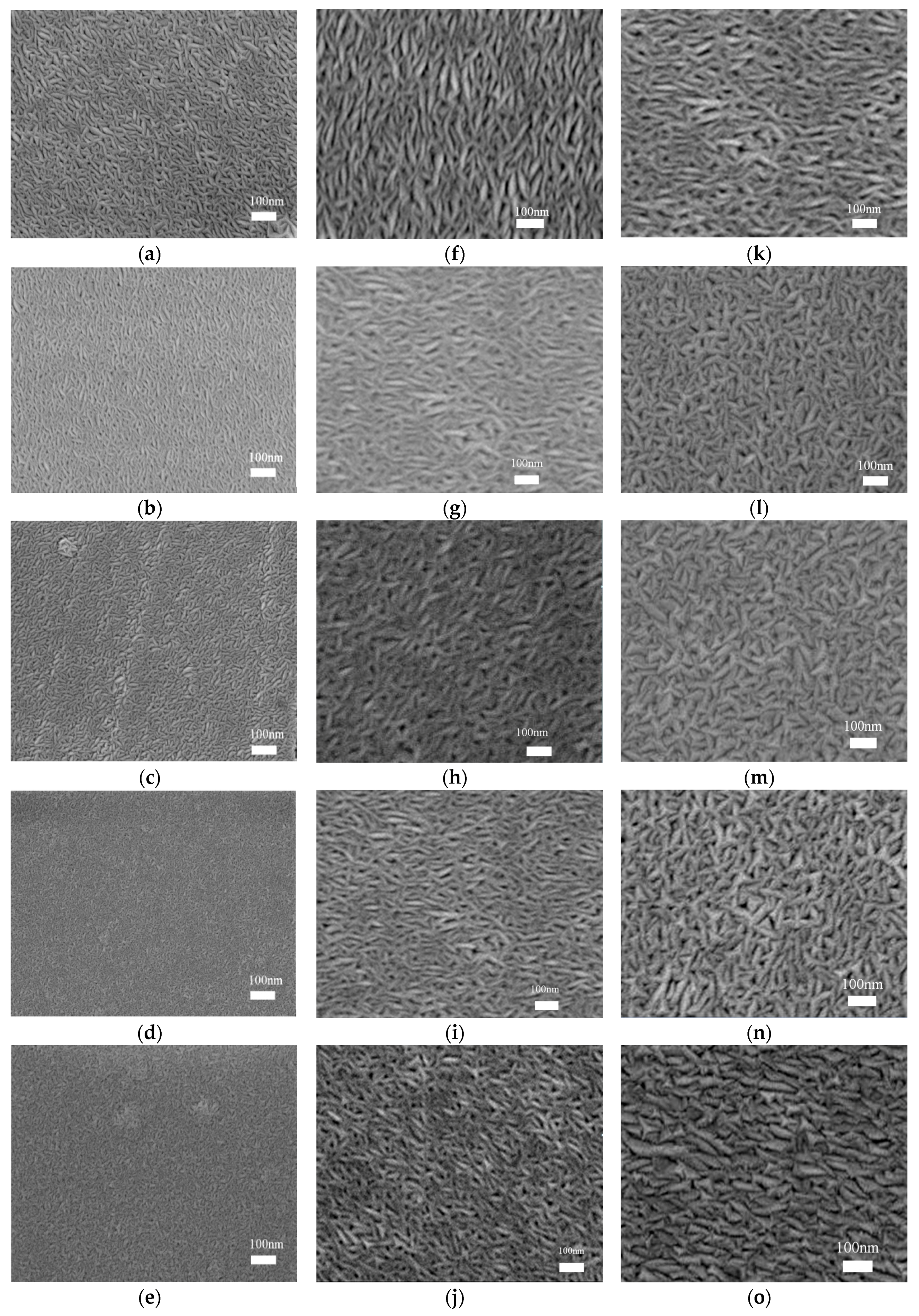
3.2. Morphological Analysis

Figure 2 shows SEM images of bottom layer Mo films prepared at different sputtering pressures (Figure 2a–e), Mo bilayer films prepared by RF/DC sputtering at different bottom layer sputtering pressures (Figure 2f–j), and Mo bilayer films with a bottom layer sputtering pressure of 0.4 Pa and top layer sputtering pressure of 0.3 Pa annealed at different annealing temperatures (Figure 2k–o). It is showed that the bottom layer Mo films prepared at different sputtering pressures consisted of spindle nanoparticles. With increasing bottom layer sputtering pressures, the grain sizes of bottom layer Mo films decreased, the uniformity of grain distribution decreased, agglomeration occured, gaps and voids increased, and the RMS roughness increased gradually (Table 1). As mentioned in the above XRD results, the Mo particles of bottom layer Mo films prepared at higher sputtering pressure underwent more collisions with Ar atoms and had less kinetic energy, which weakened grain nucleation and growth of bottom layer Mo films. All the Mo bilayer films prepared by RF/DC sputtering at different bottom layer sputtering pressures also consisted of spindle nanoparticles with uniform distribution. The length of spindles were about 120 nm, the main changes were the width of the spindles. With decreasing bottom layer sputtering pressures, the width of the spindles of Mo bilayer films increased gradually, and the voids and the root mean square (RMS) roughness decreased (Table 1). As mentioned above, the lower bottom layer sputtering pressure caused higher kinetic energy of Mo particles and then promoted the diffusion and growth of Mo particles, resulting in larger grain sizes, denser surfaces and lower RMS roughness and lower microvoids and/or vacancies in the bottom layer Mo films. This resulted in higher thermal stability of bottom layer Mo films prepared at lower sputtering pressure compared to those prepared at higher bottom layer sputtering pressure, which is particularly beneficial for the growth of top layer Mo films and the lattice matching between the bottom layer and the top layer is better, which is more conducive to the growth of Mo bilayer films. During the bombardment of top layer particles at the same sputtering conditions, less undesirable crystallographic defects escaped from the bottom layer prepared at lower sputtering pressure, resulting in an increase of the crystal quality and grain sizes of the Mo bilayer film. SEM images of Mo bilayer films with a bottom layer sputtering pressure of 0.4 Pa and top layer sputtering pressure of 0.3 Pa annealed at different temperatures are illustrated in Figure 2k–o. All the Mo bilayer films showed a uniform distribution of nanoparticles, with increasing annealing temperatures, the width of the particles increased, gaps and voids decreased. This is because, as the annealing temperature increased, the energy absorbed by Mo particles increased, the diffusibility and mobility enhanced, the combining ability with adjacent grains and nucleation ability of Mo grains increased. Therefore, with increasing annealing temperature, the width of the particles increased, the surface was more uniform and compact, and RMS roughness decreased gradually.
Figure 3 shows the grain size (width of the particle) distribution as a function sputtering pressure and annealing temperature, which were obtained by nano measurer software. Most of the grains size distribution of Mo films showed normal distribution. Only a few of the grains size distribution of bottom layer Mo films prepared at higher sputtering pressure were slightly deviated, which were mainly related to the higher sputtering pressure and shorter sputtering time. Thus the particles in Mo films do not have sufficient energy and time for nucleation and growth.
The trend obtained in the width of the particle is more or less in agreement with the grain size variation observed with an X-ray diffraction analysis. However, the discrepancy observed in the grain size values from an X-ray diffraction and scanning electron microscopy imaging analysis could be attributed to the fact that X-ray diffraction is more sensitive to intragrain dislocations and low angle grain boundaries, and the scanning electron microscope mostly measure the distance between visible grain boundaries in the microstructure [25,26]. The evolution of microstructure, grain size and compactness with sputtering process parameters (sputtering pressure and annealing temperature) is usually explained by comparing the microstructure with structure zone model for films deposited by magnetron sputtering [27]. The X-ray diffraction technique measures the crystalline region that coherently diffracts X-rays and is known to be the more precise technique for grain size determination [28].

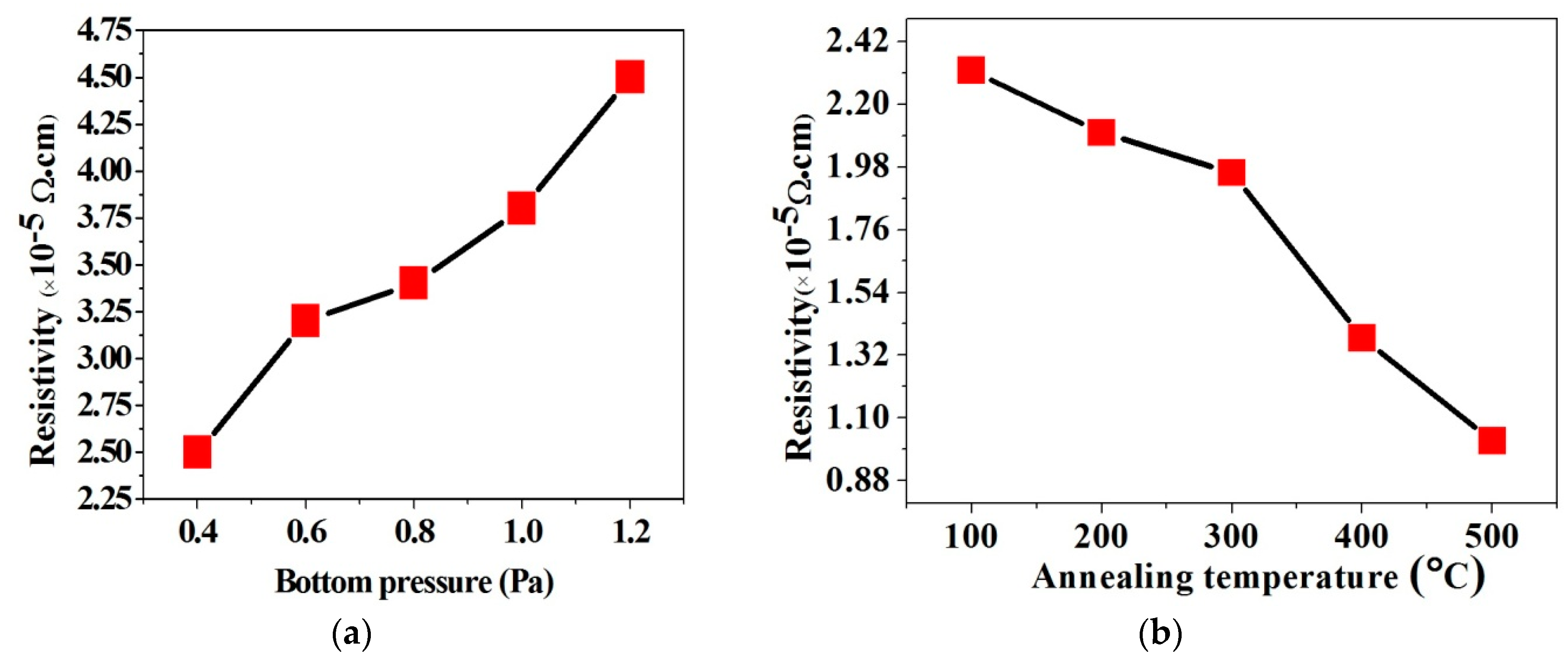
3.3. Electrical Properties

Figure 4 shows the resistivity variation of Mo bilayer films prepared at different bottom layer sputtering pressures (Figure 4a) and annealing temperatures (Figure 4b). It can be seen that the resistivity of the Mo bilayer films decreased with decreasing bottom layer sputtering pressures and increasing annealing temperatures. The average micro-strain (ε) and the dislocation density ( ρ ) (Table 1) also decreased with decreasing bottom sputtering pressures and increasing annealing temperatures, which can directly decrease the resistivity of Mo bilayer films. The resistivity is mainly related to electron scattering caused by various structural defects, including dislocations, impurities, micro-strains, grain boundaries and point defects [29]. Grain boundaries are often considered to be the main source of dislocation density, and the dislocation density is proportional to the micro-strain [30]. Therefore, with decreasing sputtering pressures and increasing annealing temperatures, the kinetic energy of Mo particles increased and the grain sizes increased. Accordingly, the number of grain boundaries decreased, the dislocation density and the micro-strain decreased, and carrier lifetime and Hall mobility increased, so the corresponding resistivity decreased.

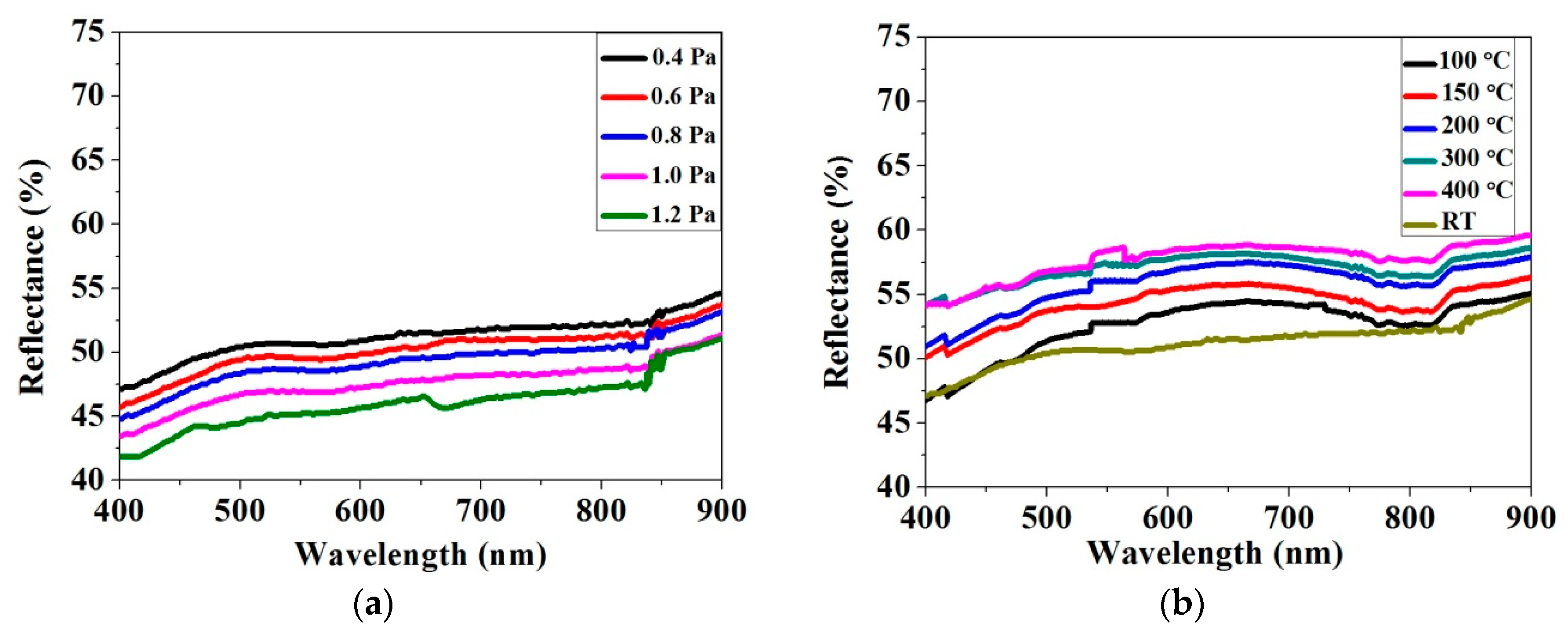
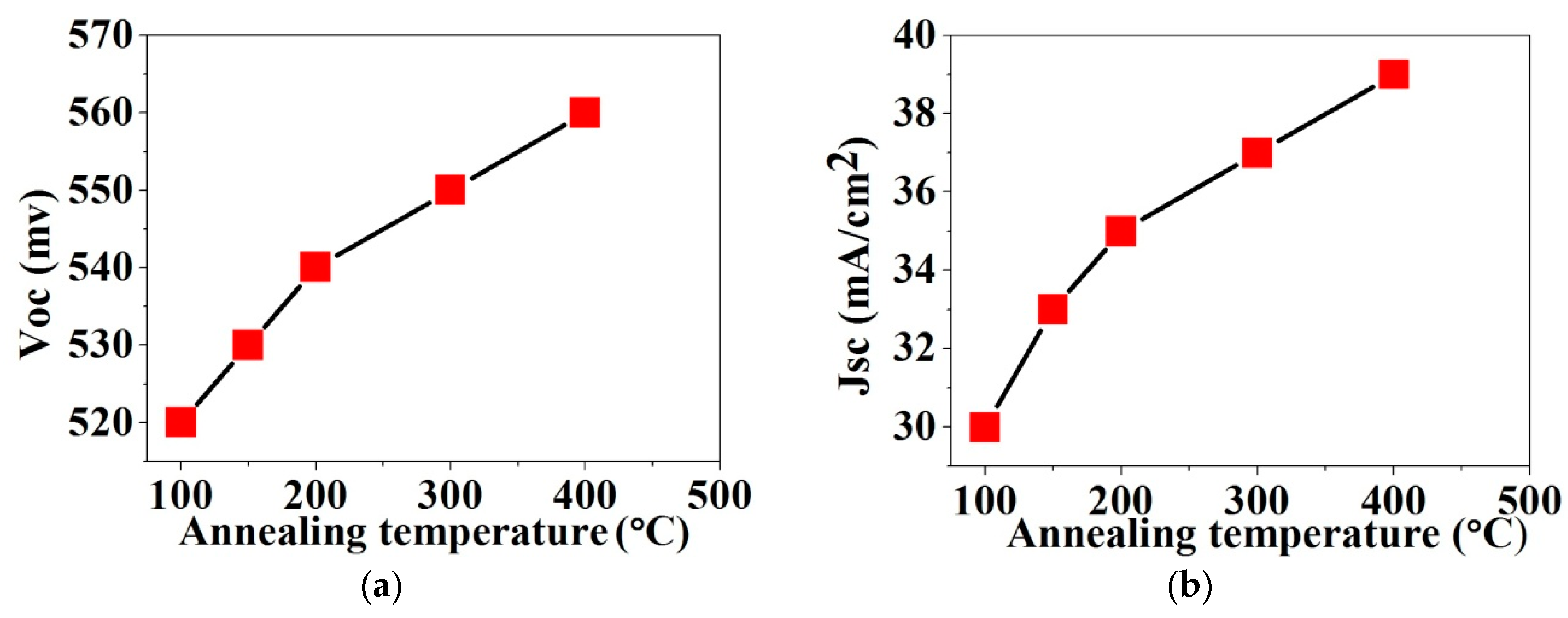
3.4. Optical Properties

The reflectance of Mo bilayer film is also a crucial parameter for the photo-conversion efficiency of a solar cell. Maximizing the light reflectance of the Mo bilayer film allows more photons to be absorbed [31]. Figure 5 shows that the reflectance of Mo bilayer film increased with decreasing bottom layer sputtering pressures and increasing annealing temperatures. This can be attributed to the fact that the Mo bottom layer films prepared at lower bottom layer sputtering pressure were more uniform and compact, and had lower RMS roughness (Table 1). Therefore, the top layer Mo film deposited on the Mo bottom layer film prepared at lower bottom layer sputtering pressure at the same sputtering conditions had the lower RMS roughness; accordingly, the reflectance of the Mo bilayer film was higher. Similar conclusions have been discussed in earlier reports [21]. For Mo bilayer films annealed at different temperatures, with increasing annealing temperatures, the particle energy of Mo bilayer films increased gradually, and the prepared Mo bilayer films were more uniform and compact having lower RMS roughness (Table 1), which reduced light scattering and absorption of Mo bilayer films. This brought about higher reflectance.
The experimental results show that the Mo bilayer film prepared at lower bottom layer sputtering pressure and higher annealing temperature has the better properties. CIGS absorbers were deposited on these Mo bilayer films with bottom layer sputtering pressure of 0.4 Pa, top layer sputtering pressure of 0.3 Pa and annealed at different temperatures via a 3-stage co-evaporation [32]. Then, cadmium sulphide (CdS) buffer layers were prepared by chemical bath deposition (CBD), intrinsic zinc oxide (i-ZnO)/n-type indium tin oxide (ITO) window layers were obtained through the sputtering method, and the Al grid electrode was evaporated in order. Figure 6 shows the current–voltage (I–V) parameters as a function of annealing temperature of Mo electrodes. The results show that the open circuit voltages (Voc), short circuit current densities (Jsc), the fill factors (FF) and photo-conversion efficiencies of the CIGS solar cells increased with increasing annealing temperature. This mainly originated from the fact that the reflectance and light absorption of Mo bilayer film increased and the resistivity decreased with increasing annealing temperature. The Mo bilayer film annealed at 400 °C demonstrated excellent comprehensive performance: its resistivity reached to 0.92 × 10⁻⁵ Ω.cm and the reflectance was above 55%, the maximum photo-conversion efficiency of 13.5% was achieved for the CIGS solar cell.

4. Conclusions

In summary, the effects of bottom layer sputtering pressures and annealing temperatures on the microstructures and properties of Mo bilayer films prepared by RF/DC magnetron sputtering were investigated. The results show that both the bottom layer sputtering pressures and annealing temperatures have great influences on the structures and properties of Mo bilayer films. The sputtering kinetic energy and mobility of Mo particles in Mo films increased with decreasing sputtering pressures and increasing annealing temperatures, leading to the increase of grain sizes, uniformity and compactness of Mo films and the decrease of RMS roughness. Correspondingly, the electrical conductivity and reflectance of Mo bilayer films were also increased. Resistivity ranging from 2.40 to 4.62 × 10⁻⁵ Ω.cm was obtained at 0.4 to 1.2 Pa bottom layer sputtering pressure and 2.31 to 0.92 × 10⁻⁵ Ω.cm at 100 to 400 °C annealing temperature. The strain decreased with increasing annealing temperatures and bottom layer sputtering pressures. Moreover, the particles’ morphology of Mo bilayer films changed from spindles to triangles with increasing annealing temperatures. Prepared Mo bilayer films exhibited better adhesion, higher reflectance and lower resistivity which could be used suitably for the back electrode of CIGS solar cells. The Mo bilayer film prepared at 0.4 Pa of bottom layer sputtering pressure, 0.3 Pa of top layer sputtering pressure and annealed at 400 °C demonstrated excellent comprehensive performance: its resistivity reached 0.92 × 10⁻⁵ Ω.cm, the reflectance was above 55%, and the maximum photo-conversion efficiency of 13.5% was achieved for the CIGS solar cell. From the above results, we can see that under the same sputtering conditions, the adhesion and reflectance of Mo bilayer films prepared by RF/DC mode were higher than that of DC/DC mode, and the conductivity and efficiency of CIGS solar cells were close to that of DC/DC mode.

Author Contributions

Conceptualization, data curation, formal analysis, validation and writing—original draft (H.Z.); Conceptualization, funding acquisition, methodology, project administration (J.X.); Conceptualization, formal analysis, investigation and writing—review and editing (A.M.).

Funding

This research was funded by the Key Project of Education Department of Henan Province (grant number 17A430018), the Key Research Project of Henan Colleges and Universities (grant number 18B430008).

Conflicts of Interest

The authors declare no conflict of interest.

References

  1. Tang, H.; Zhang, H.; Chen, L.; Guo, S. Novel laser rapidly solidified medium-entropy high speed steel coatings with enhanced hot wear resistance. J. Alloys Compd. 2018, 772, 719–727. [Google Scholar] [CrossRef]
  2. Liu, X.Z.; Ning, H.L.; Chen, W.F.; Fang, Z.Q.; Yao, R.H.; Wang, X.F.; Deng, Y.X.; Yuan, W.J.; Wu, W.J.; Peng, J.B. Effect of source/drain electrodes on the electrical properties of silicon-tin oxide thin-film transistors. Nanomaterials 2018, 8, 293. [Google Scholar] [CrossRef]
  3. Choi, D. The potential of molybdenum and nickel as next-generation semiconductor interconnects. Nanosci. Nanotechnol. Lett. 2018, 10, 1310–1314. [Google Scholar] [CrossRef]
  4. Cho, Y.; Jeong, I.; Gang, M.G.; Kim, J.H.; Song, S.; Eo, Y.J.; Ahn, S.K.; Shin, D.H.; Cho, J.S.; Yun, J.H. Alkali incorporation into Cu(In,Ga)Se2 determined by crystal orientation of Mo back contact: Implications for highly efficient photovoltaic devices. Sol. Energy Mater. Sol. Cells 2018, 188, 46–50. [Google Scholar] [CrossRef]
  5. Wang, S.S.; Hsu, C.Y.; Shiou, F.J.; Huang, P.C.; Wen, D.C. Properties of the Mo back contact for the formation of a thin-film photovoltaic absorber. J. Electron. Mater. 2013, 42, 71–77. [Google Scholar] [CrossRef]
  6. Yang, W.; Rossnagel, S.M.; Joo, J. The effects of impurity and temperature for transparent conducting oxide properties of Al:ZnO deposited by DC magnetron sputtering. Vacuum 2012, 86, 1452–1457. [Google Scholar] [CrossRef]
  7. Zhou, D.; Zhu, H.; Liang, X. Sputtered molybdenum thin films and the application in CIGS solar cells. Appl. Surf. Sci. 2016, 362, 202–209. [Google Scholar] [CrossRef]
  8. Zhao, H.; Xie, J.; Mao, A.; Wang, A.; Chen, Y.; Liang, T.; Ma, D. Effects of heating mode and temperature on the microstructures, electrical and optical properties of molybdenum thin Films. Materials 2018, 11, 1634. [Google Scholar] [CrossRef] [PubMed]
  9. Akçay, N.; Akın, N.; Cömert, B.; Özçelik, S. Temperature effects on the structural, optical, electrical and morphological properties of the RF-sputtered Mo thin films. J. Mater. Sci. Mater. Electron. 2017, 28, 399–406. [Google Scholar] [CrossRef]
  10. Akcay, N.; Akin Sonmez, N.; Zaretskaya, E.P.; Ozcelik, S. Influence of deposition pressure and power on characteristics of RF sputtered Mo films and investigation of sodium diffusion in the films. Curr. Appl. Phys. 2018, 18, 491–499. [Google Scholar] [CrossRef]
  11. Nwakanma, O.; Reyes, P.; Velumani, S. Electrical, structural, and topographical properties of direct current (DC) sputtered bilayer molybdenum thin films. J. Mater. Sci. Mater. Electron. 2018, 29, 15671–15681. [Google Scholar] [CrossRef]
  12. Scofield, J.H.; Duda, A.; Albin, D.; Ballard, B.L.; Predecki, P.K. Sputtered molybdenum bilayer back contact for copper indium diselenide-based polycrystalline thin-film solar cells. Thin Solid Films 1995, 260, 26–31. [Google Scholar] [CrossRef]
  13. Huang, P.C.; Sung, C.C.; Chen, J.H.; Huang, C.H.; Hsu, C.Y. The optimization of a Mo bilayer and its application in Cu(In,Ga)Se2 solar cells. Appl. Surf. Sci. 2017, 425, 24–31. [Google Scholar] [CrossRef]
  14. Badgujar, A.C.; Dhage, S.R.; Joshi, S.V. Process parameter impact on properties of sputtered large-area Mo bilayers for CIGS thin film solar cell applications. Thin Solid Films 2015, 589, 79–84. [Google Scholar] [CrossRef]
  15. Zhu, H.; Dong, Z.; Niu, X.; Li, J.; Shen, K.; Mai, Y.; Wan, M. DC and RF sputtered molybdenum electrodes for Cu(In,Ga)Se2 thin film solar cells. Appl. Surf. Sci. 2019, 465, 48–55. [Google Scholar] [CrossRef]
  16. Feng, J.; Wu, Z.; Wang, W.; Yuan, Y.; Zhuang, L.; Wang, X.; Hong, R.; Shen, H.; Michael, Z.Q. Preparation and optimization of a molybdenum electrode for CIGS solar cells. AIP Adv. 2016, 6, 115210. [Google Scholar] [CrossRef] [Green Version]
  17. Poncelet, O.; Kotipalli, R.; Vermang, B.; Macleod, A.; Francis, L.A.; Flandre, D. Optimisation of rear reflectance in ultra-thin CIGS solar cells towards >20% efficiency. Sol. Energy 2017, 146, 443–452. [Google Scholar] [CrossRef]
  18. Raneourt, J.D. Optical Thin Films User Handbook; SPIE: Belingham, WA, USA, 1996; p. 160. [Google Scholar]
  19. Morgan, M.J.; Jakovidis, G.; McLeod, I. An experiment to measure the I-V characteristics of a silicon solar cell. Phys. Educ. 1994, 252–254. [Google Scholar] [CrossRef]
  20. Patterson, A.L. The scherrer formula for X-Ray particle size determination. Phys. Rev. 1939, 15, 978–982. [Google Scholar] [CrossRef]
  21. Ahmadipour, M.; Cheah, W.K.; Ain, M.F.; Rao, K.V.; Ahmad, Z.A. Effects of deposition temperatures and substrates on microstructure and optical properties of sputtered CCTO thin film. Mater. Lett. 2018, 210, 4–7. [Google Scholar] [CrossRef]
  22. Wu, H.M.; Liang, S.C.; Lin, Y.L.; Ni, C.Y.; Bor, H.Y.; Tsai, D.C.; Shieu, F.S. Structure and electrical properties of Mo back contact for Cu(In, Ga)Se2 solar cells. Vacuum 2012, 86, 1916–1919. [Google Scholar] [CrossRef]
  23. Guillaume, Z.; Neil, S.; Jonathan, D.M.; Robert, W.M.; Ian, F. Electrical, morphological and structural properties of RF magnetron sputtered Mo thin films for application in thin film photovoltaic solar cells. J. Mater. Sci. 2011, 46, 4913–4921. [Google Scholar] [CrossRef] [Green Version]
  24. Jia, X.; Lin, Z.; Yang, T.C.; Binesh, P.V.; Wu, L.; Gavin, C.; Ivan, P.W. Post-sputtering heat treatments of molybdenum on silicon wafer. Appl. Sci. 2018, 8, 1692. [Google Scholar] [CrossRef]
  25. Khranovskyy, V.; Grossner, U.; Nilsen, O.; Lazorenko, V.; Lashkarev, G.V.; Svensson, B.G.; Yakimova, R. Structural and morphological properties of ZnO: Ga thin films. Thin Solid Films 2006, 515, 472–476. [Google Scholar] [CrossRef]
  26. Lu, J.G.; Ye, Z.Z.; Zeng, Y.J.; Zhu, L.P.; Wang, L.; Yuan, J.; Zhao, B.H.; Liang, Q.L. Structural, optical, and electrical properties of (Zn, Al) O films over a wide range of compositions. J. Appl. Phys. 2006, 100, 073714. [Google Scholar] [CrossRef]
  27. Kluth, O.; Schöpe, G.; Hüpkes, J.; Agashe, C.; Müller, J.; Rech, B. Modified thornton model for magnetron sputtered zinc oxide: Film structure and etching behaviour. Thin Solid Films 2003, 442, 80–85. [Google Scholar] [CrossRef]
  28. Sharma, A.; Mohan, S.; Suwas, S. The influence of deposition temperature on the structure,microstructure, morphology and magnetic properties of sputter deposited nickel thin films. Thin Solid Films 2016, 619, 91–101. [Google Scholar] [CrossRef]
  29. Yoon, J.H.; Cho, S.; Kim, W.M. Optical analysis of the microstructure of a Mo back contact for Cu(In,Ga)Se2 solar cells and its effects on Mo film properties and Na diffusivity. Sol. Energy Mater. Sol. Cells 2011, 95, 2959–2964. [Google Scholar] [CrossRef]
  30. Watts, B.R. Calculation of electrical resistivity produced by dislocations in various metals. J. Phys. F Met. Phys. 1988, 18, 1197–1209. [Google Scholar] [CrossRef]
  31. Jubault, M.; Ribeaucourt, L.; Chassaing, E.; Renou, G.; Lincot, D.; Donsanti, F. Optimization of molybdenum thin films for electrodeposited CIGS solar cells. Sol. Energy Mater. Sol. Cells 2011, 95, S26–S31. [Google Scholar] [CrossRef]
  32. Gabor, A.M.; Tuttle, J.R.; Bode, M.H.; Franz, A.; Tennant, A.L.; Contreras, M.A.; Noufi, R.; Jensen, D.G.; Hermann, A.M. Bandgap engineering in Cu(In,Ga)Se2 thin films grown from (In,Ga)2Se3 precursors. Sol. Energy Mater. Sol. Cells 1996, 41–42, 247–260. [Google Scholar] [CrossRef]
Figure 1. X-ray diffraction (XRD) patterns of Mo bilayer films (a) deposited at different bottom layer sputtering pressures and (b) annealed at different temperatures.
Applsci 09 01395 g001
Figure 2. Scanning electron microscope (SEM) images of bottom layer Mo films deposited at different bottom layer sputtering pressures: (a) 0.4 Pa, (b) 0.6 Pa, (c) 0.8 Pa, (d) 1.0 Pa, (e) 1.2 Pa, Mo bilayer films deposited at different sputtering pressures: (f) 0.4 Pa, (g) 0.6 Pa, (h) 0.8 Pa, (i) 1.0 Pa, (j) 1.2 Pa and Mo bilayer films annealed at different temperatures: (k) 100 °C, (l) 150 °C, (m) 200 °C, (n) 300 °C, and (o) 400 °C.
Applsci 09 01395 g002
Figure 3. Grain size distribution of bottom layer Mo films deposited at different bottom layer sputtering pressures: (a) 0.4 Pa, (b) 0.6 Pa, (c) 0.8 Pa, (d) 1.0 Pa, (e) 1.2 Pa, Mo bilayer films deposited at different bottom layer sputtering pressures: (f) 0.4 Pa, (g) 0.6 Pa, (h) 0.8 Pa, (i) 1.0 Pa, (j) 1.2 Pa and Mo bilayer films annealed at different temperatures: (k) 100 °C, (l) 150 °C, (m) 200 °C, (n) 300 °C, and (o) 400 °C.
Applsci 09 01395 g003
Figure 4. Resistivity of Mo bilayer films deposited at different bottom sputtering pressures (a) and annealed at different temperatures (b).
Applsci 09 01395 g004
Figure 5. Reflectance of Mo bilayer films (a) deposited at different bottom layer sputtering pressures and (b) annealed at different temperatures.
Applsci 09 01395 g005
Figure 6. I–V parameters of copper indium gallium selenium (CIGS) solar cells as a function of annealing temperature of Mo electrodes: (a) change of the open circuit voltage (Voc) with different annealing temperature; (b) change of the short circuit current density (Jsc) with different annealing temperature; (c) change of the fill factor (FF) with different annealing temperature; and (d) change of the photo-conversion efficiency(η) with different annealing temperature.
Applsci 09 01395 g006aApplsci 09 01395 g006b
Table 1. Grain size, root mean square (RMS) roughness, dislocation density, micro-strain, strain and Hall mobility of Mo bilayer films deposited by radio frequency/direct current (RF/DC) (RF Mo bottom layer and DC Mo Top layer) sputtering at different bottom layer sputtering pressures, Mo bilayer films with a bottom sputtering pressure of 0.4 Pa and top sputtering pressure of 0.3 Pa annealed at different temperatures and bottom layer Mo films prepared at different sputtering pressures.
Bottom Sputtering Pressure
(Pa)
Annealing Temperature
(°C)
Grain Size (nm)RMS Roughness
(nm)
Dislocation Density
(δ) × 105 cm2
Micro-Strain
(ε) × 103
Hall Mobility (cm2/Vs)Strain (%)Top Sputtering Pressure
(Pa)
0.4 30.527.181.0743.69.861.320.3
0.6 26.367.861.4393.97.271.250.3
0.8 21.438.322.1774.36.351.230.3
1.0 18.528.982.9164.85.251.190.3
1.2 17.1210.233.4125.23.961.100.3
0.410033.256.350.9053.410.131.050.3
0.415038.526.180.6743.211.060.980.3
0.420040.345.780.6152.912.020.950.3
0.430043.634.730.5252.612.830.900.3
0.440047.283.360.4472.213.580.840.3
0.4 15.235.222.1226.26.321.12
0.6 14.085.962.5366.75.831.02
0.8 12.356.283.1257.15.060.89
1.0 11.227.024.5347.54.140.82
1.2 10.367.644.9688.62.460.78

