Review of Substrate Integrated Waveguide Circuits for Beam-Forming Networks Working in X-Band
by
 ,
,
Giuseppe Venanzoni
1,* ,
,
Davide Mencarelli
2,
Antonio Morini
2,
Marco Farina
2 and
Francesco Prudenzano
3 1
Dipartimento di Ingegneria, Università di Perugia, Via G. Duranti 93, 06123 Perugia, Italy
2
Dipartimento di Ingegneria dell’Informazione, Università Politecnica delle Marche, Via Brecce Bianche, 60131 Ancona, Italy
3
Dipartimento di Ingegneria Elettrica e dell’Informazione, Politecnico di Bari, Via Orabona, 70100 Bari, Italy
*
Author to whom correspondence should be addressed.
Appl. Sci. 2019, 9(5), 1003; https://doi.org/10.3390/app9051003
Submission received: 8 February 2019
/
Revised: 28 February 2019
/
Accepted: 5 March 2019
/
Published: 11 March 2019
(This article belongs to the Special Issue Substrate Integrated Waveguide (SIW) and Its Applications)
Abstract
:A review of substrate integrated waveguide (SIW) components designed for the use in beam-forming networks working in X-Band is presented. The proposed devices are four-port and six-port couplers and magic tees for the network. The devices take full advantage of the use of SIW technology in order to reduce size, weight, and cost. The design processes of all devices are exposed, and the experimental results of prototypes show the feasibility of these solutions.
1. Introduction
In recent years, substrate integrated waveguide (SIW) [1,2,3] technology has gained more and more attention in the microwave community for its flexibility in the realization of microwave circuits [4].
The propagation and dispersion characteristics of SIWs are very similar to those of rectangular waveguides so that the skills required for hollow waveguides can be used for SIWs. As a matter of fact, many devices designed for waveguide technology can easily be built using substrate integrated waveguides. Moreover, SIW devices are manufactured using standard printed circuit board (PCB) procedures, making them simpler to build, lighter, and less expensive than a waveguide device built with a standard process such as milling. The fact that SIW devices are realized using a dielectric substrate allows for an easy integration with other planar circuits, for example based on microstrip technology. The presence of the dielectric also allows for a shrinking of the dimensions with a scale factor proportional to the square root of the relative dielectric permittivity.
Of course, the presence of a dielectric inside the waveguide increases the losses, depending on the loss tangent of the material used. Losses are also affected by the relatively low height of the substrate waveguides, which increases the conductor losses.
Dielectric losses can be reduced by using substrates with low loss tangent, though these substrates are more expensive. Conductor losses can also be decreased by using thicker substrates, thus affecting the size, weight, and cost of the device. These problems are mitigated for wide-band devices and signal-level circuits, where additional losses can be compensated by the use of amplifiers.
Another drawback of SIW devices compared to standard waveguide ones is the limited power handling resulting from the reduced height of the waveguide.
In this contribution, a review of devices designed and built for X-band applications is presented. More specifically, the devices have been designed to be used in satellite digital video broadcast (DVB-S) applications as an alternative to existing dish antennas. The goal is to have a series of devices that are thinner, lighter, and have less visual impact, compared to dish antennas. In order to keep the cost of the appliances low, particular attention must be devoted to the choice of the substrates. Very low-cost FR4 substrates are not suitable for microwave devices, since there are high losses and big uncertainties about its dielectric permittivity. Other substrates, such as Rogers RT/duroid® 5870/5880, are very good at microwave frequencies and exhibit very low dispersions of characteristics over different samples. However, they are very expensive, and they are also not suitable for the application under examination. There are some mid-level substrates, such as the Taconic RF-35, used in nearly all the prototypes illustrated in this review that are particularly suited for big antennas. They are relatively low-cost, and they show very good behavior in terms of their losses and their uniformity in electrical parameters over samples.
This situation can change in the future by the advent of new technologies, such as metamaterials [5,6,7,8,9,10], that promise better characteristics thanks to artificial materials.
The manuscript is divided as follows. In Section 2 some fundamental theories about SIWs are presented, and in Section 3 a number of devices for beam-forming networks are illustrated. In Section 4 an array antenna for DVB-S application is designed and measured. Finally, in Section 5 a new fabrication process for empty SIWs is proposed in order to build devices that are not affected by dielectric losses.
2. Fundamental Theory
Figure 1 shows an illustration of a substrate integrated waveguide with the main dimensions.
The propagation inside a SIW strongly resembles the propagation inside a classical hollow waveguide with some important differences. In fact, the propagating modes are very close to the TEn0 modes of the waveguide, as they are the fundamental mode of the TE10. Since the height of the substrate waveguide is very small, the cutoff frequency of the TEmn modes with n ≥ 1 is shifted to very high frequencies and usually are not taken into consideration. Moreover, the gaps on the lateral walls prevent the propagation of TM modes [11,12] because the strong radiation does not allow longitudinal currents.
In the literature there are some empirical formulas that relate the size of a SIW with an equivalent, or effective, waveguide with continuous lateral walls. One of the most commonly used is [13]:
where w is the width of the SIW, d is the diameter of the vias, and s is the spacing among vias (see Figure 1). Weff is the effective width of a rectangular waveguide with the same propagation characteristic, i.e., same propagation constant and electromagnetic field profile. This formula allows the design of devices using and equivalent waveguide with continuous lateral walls, thus simplifying the synthesis process.
From Equation (1), the cutoff frequency of the TE10 mode can be easily computed using the following:
These formulas are very accurate when:
Other formulas have been proposed, by using different analytical or numerical methods [14,15,16], improving the accuracy over a wider range of the d/w ratio.
There are three different mechanisms that cause losses in SIW [17,18]: conductor losses, dielectric losses, and radiation. Conductor losses depend on the metal used (usually copper), the roughness of the metal, and the height of the SIW. The first two cannot be directly controlled by the designer since they depend on the quality of the copper lamination of the substrate. Of course the thickness of the metallization should be suitably chosen depending on the frequency and the skin depth. On the other hand, the thicker the substrate is, the lower the losses are, so there is a tradeoff between the losses and the size and weight of the final device, especially in the case of multilayer PCBs. Dielectric losses depend only on the quality of the substrate because they are independent on the cross-section of the waveguide. The choice of the substrate is always a tradeoff between performance and cost. Radiation losses are caused by the scattering from noncontiguous lateral walls. Negligible radiation losses occur when the diameter of the vias is big enough and the spacing among them is small enough. An empirical formula can be used to set the via spacing dependent on the diameter [18]:
3. Components for the Beam-Forming Network
The beam-forming network (BFN) is a microwave network that processes the input signal in order to feed an array antenna in such a way to generate a given radiation pattern. BFNs can be very complicated, especially when the antenna elements must be fed by signals with different amplitudes and phases. Things become much worse when the same antenna must generate different beams, for example, with different main lobe directions. However, for the topic of antennas for DVB-S, the elements of the array are fed by signals of the same amplitude and phase, generating a broadside main lobe. This also maximizes the gain of the antenna. The drawback is that the side lobes are not at their minimum level. The main elements of a BFN are dividers, four-port couplers, magic tees, and six-port couplers. In the following, some structures are presented.
3.1. Four-Port Directional Coupler
One of the basic building blocks of a BFN is the four-port directional coupler. There are many examples of SIW couplers made using quite expensive substrates, such as Rogers RT/duroid® 5870/5880 [19,20,21,22,23,24,25,26]. The main goal of using a Rogers RT/duroid® substrate is to reduce as much as possible the dielectric losses. However, an antenna for a DVB-S signal is quite big, i.e., comparable with the size of a commonly used dish antenna, and should be low-cost. In order to accomplish these specifications, a less expensive substrate was used for this study. In particular, the chosen substrate was the Taconic RF-35 (εr = 3.5), which exhibits a nominal loss tangent equal to 0.002. Moreover, the higher dielectric permittivity compared to Rogers RT/duroid® substrates can be exploited to reduce the size of the circuits.
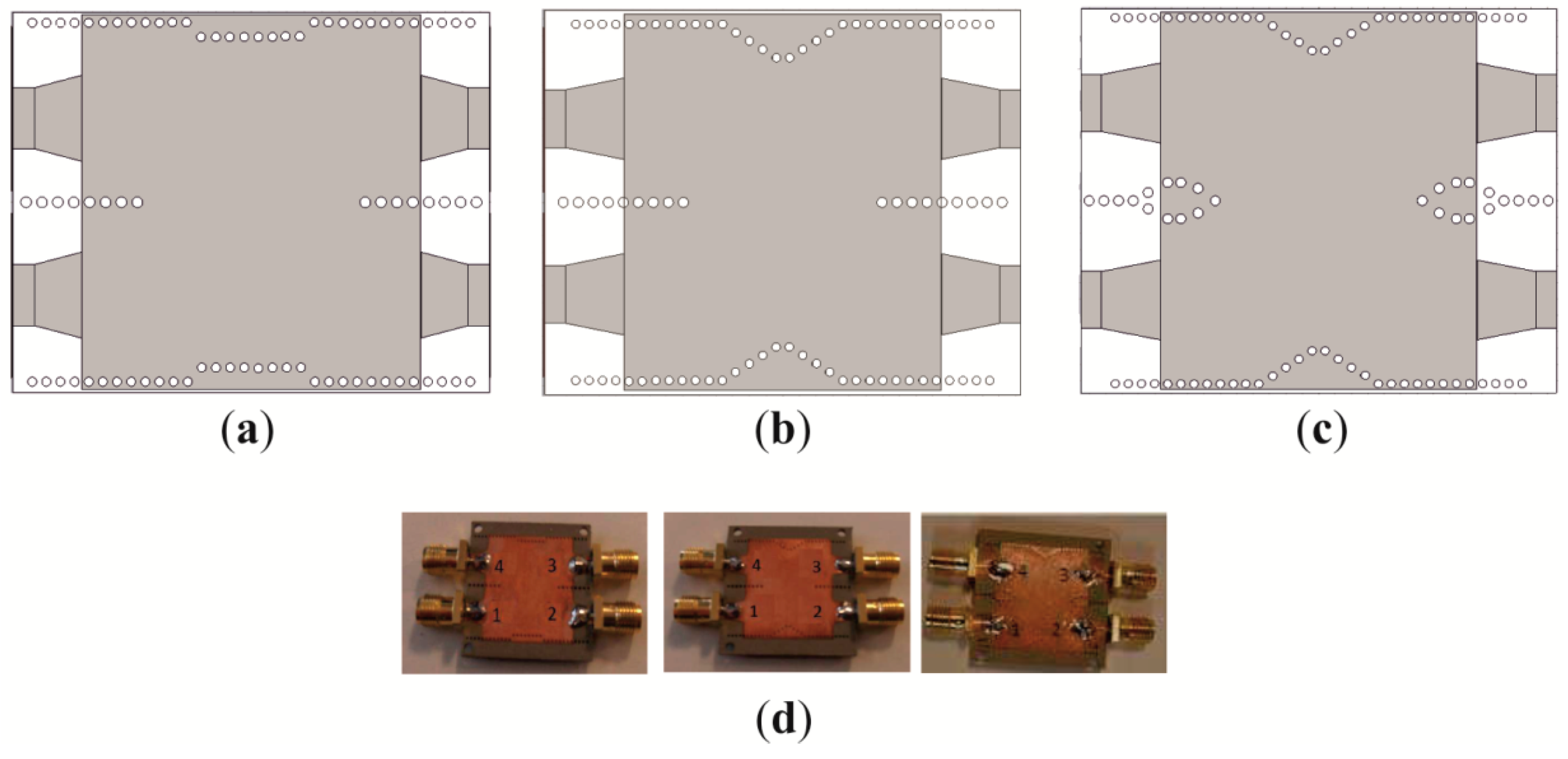
The coupling coefficient of a directional coupler can be different depending on the application. For example, prototypes with a coupling of 3 dB, 6 dB, and 10 dB have been realized [19]. The most common coupler structure used for SIW realization is the Riblet coupler [27]. This device is very simple since it can easily be built using a single dielectric layer. The coupler in [19] was a good example, but it operated in K band. In [28,29], an in-depth investigation of directional couplers made with RF-35 substrate was done. The study analyzed state-of-the-art existing devices available in the literature. It adapted the results to the new substrate and improved the frequency response in order to obtain the desired coupling coefficient over a bandwidth from 10.5 GHz to 12.5 GHz. In [29], this was done by first scaling the device in order to have a TE10 cut-off frequency at nearly 9 GHz, then, by changing the shape of the waveguide walls in order to improve the matching and adjust the coupling. In the aforementioned study, eight different couplers were designed using two different thicknesses of the substrate. The first group of four couplers used a 0.5 mm-thick substrate, whereas the second group used a 1.52 mm-thick substrate. For both groups the starting point was a coupler with straight lateral walls, as the one proposed in [19]. The best results were obtained for the second group.
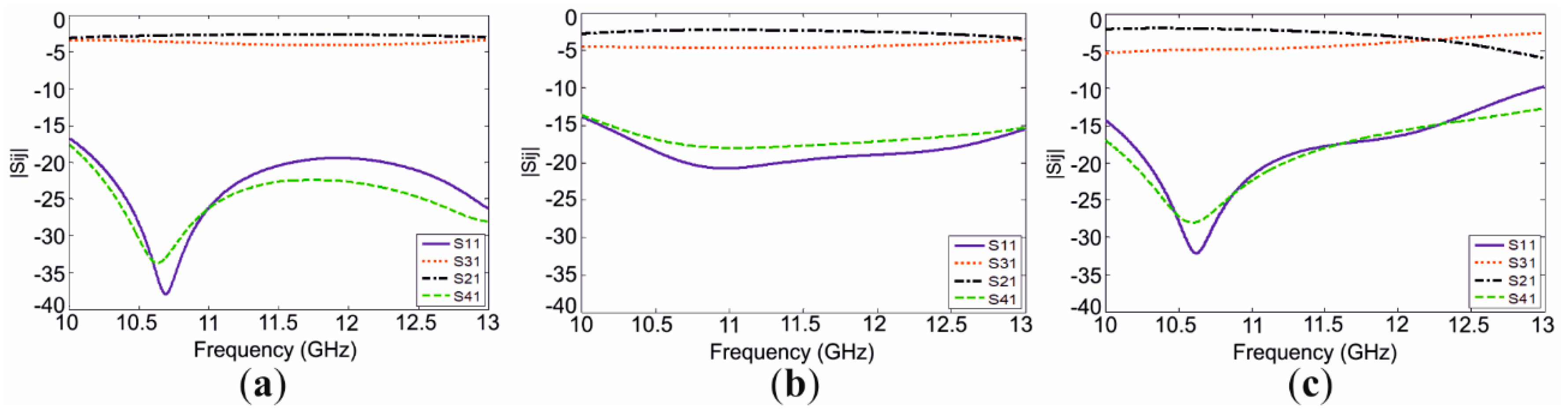
Three prototypes were built (Figure 2) corresponding to coupler #6, #7, and #8, as described in the article [29]. They exhibited the best performances in terms of bandwidth, return loss, and coupling balance. These results have been obtained by tapering the shape of the lateral walls of the couplers in different ways. As can be seen by the photos, the connection between the devices and the SMA connectors was made by using an SIW-to-microstrip transition, as the one proposed in [1,30,31]. The experimental scattering parameters of the couplers are shown in Figure 3. All the measurements of scattering parameters were done using a Keysight PNA E8361C with TRL calibration. The results showed a low return loss and flat coupling coefficients over the band 10.7–12.7 GHz.
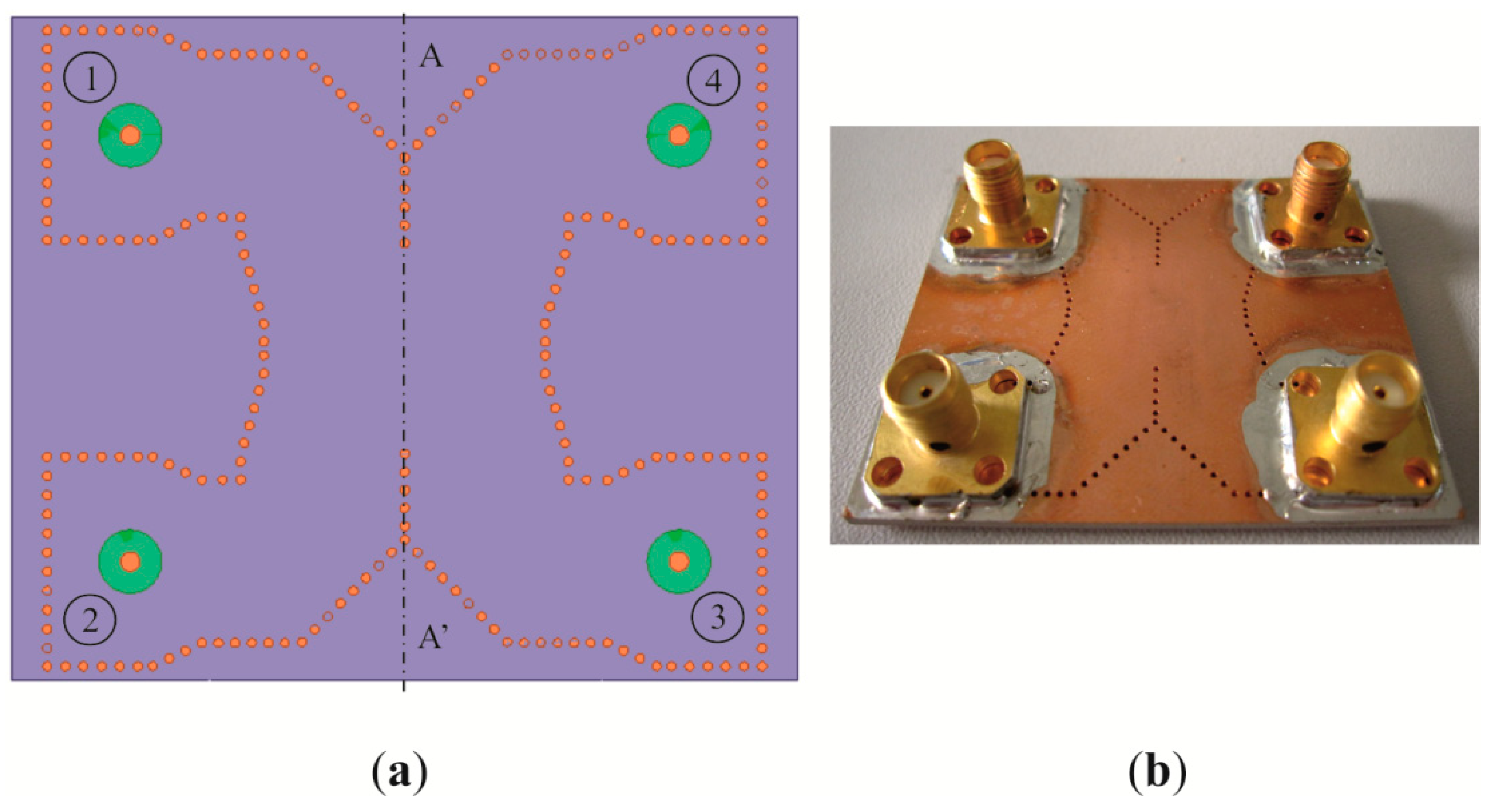
Another approach to the design was used in [32]. In this case, a 3 dB directional coupler was designed starting directly from the Riblet theory. In the coupling zone, i.e., the area where the aperture was between the two adjacent waveguides, the width of the coupler was usually lower than double the width of a single waveguide. The reason was that, in the coupling region, only two modes (TE10 and TE20) must be above cutoff in the passband of the device. The two modes were, respectively, the even and odd modes of the half structure, obtained by cutting the coupler along the symmetry plane A–A’ (Figure 4a).
Following the Riblet theory, in order to design a 3 dB coupler, the even and odd circuits must be matched, and the phase difference between the transmission coefficients in even and odd cases must be equal to 90°. Differently from the coupler shown in Figure 2, the connection between the device and the SMA connectors was made using the transition proposed in [33]. In this way, the coupler was completely closed, thus avoiding any radiation loss due to the transitions. The final size of the device was 52 × 44 mm2, whereas the core, without the transitions to SMA connectors, was 30 × 44 mm2. Looking at Figure 4, we assume that port 1 is the input, port 2 is the direct port, port 3 is the coupled port, and port 4 is the isolated one.
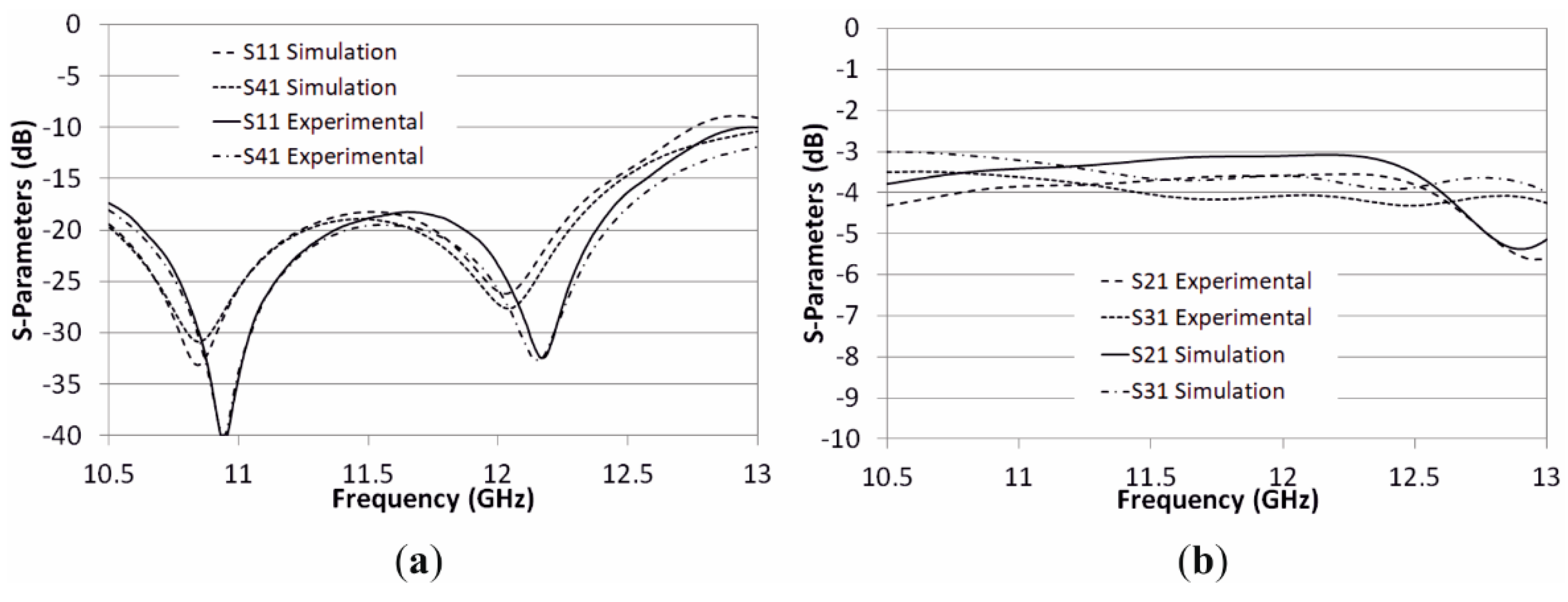
Figure 5 shows the comparison between the simulated and experimental scattering parameters for this coupler. Figure 6 shows the measured phase difference between the direct and the coupled port, which should be nominally 90°. Although the designed device was quite simple, the results showed good performances, with a good return loss over the band 10.5–12.7 GHz and a very good balance of the transmission to the direct and the coupled ports. Performances can be further improved by either adding some matching structures into the line connecting the SMA ports to the device core or by using a multi-hole coupler. For both improvements, sizes, losses, and costs will be higher than the proposed solution.
3.2. Six-Port Directional Coupler
Another device that can easily be built with a single layer SIW is the six-port directional coupler. Six-port directional couplers are not as common as the four-port counterparts. There are few examples of such devices in the literature [34,35,36]. One reason is that the circuit is quite complex to design. Moreover, the coupler can also be realized by combining standard four-port couplers and phase shifters [37,38,39,40,41,42]. However, a single block six-port coupler is more convenient because it is usually smaller and it sports a wider band. Moreover, with the proposed design, the three input ports were placed at one side of the device and the three output ports at the other side, which was more useful.
As opposed to four-port couplers, where the coupling coefficient can be different depending on the application, a six-port coupler is usually designed to divide the input power by three. This means that the scattering matrix of the device is:
where the phase is taken as reference. The simultaneous application of matching at all ports, reciprocity, no losses, and symmetry planes gives the following phase relations [34,36]:
From Equation (6), there are only two phases that can change freely.
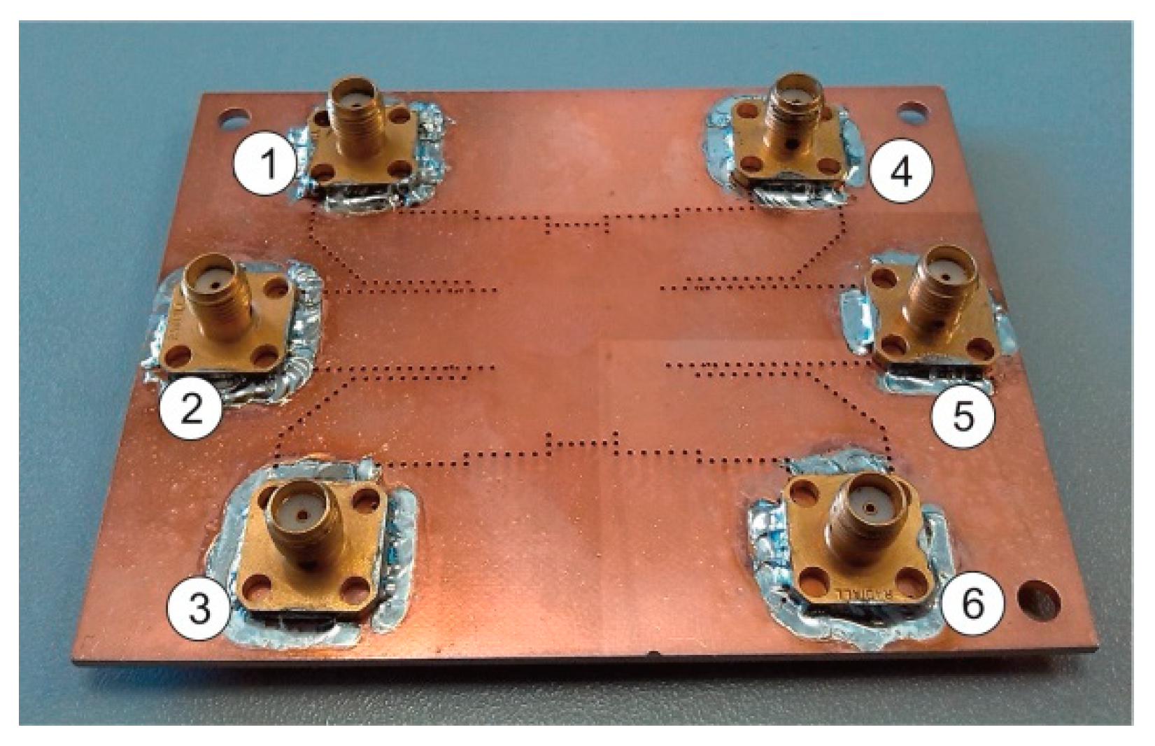
For this kind of device, there was not a known synthesis technique, so it had to be designed only by optimization. The performances obtained for the X-band coupler (Figure 7) were quite good.
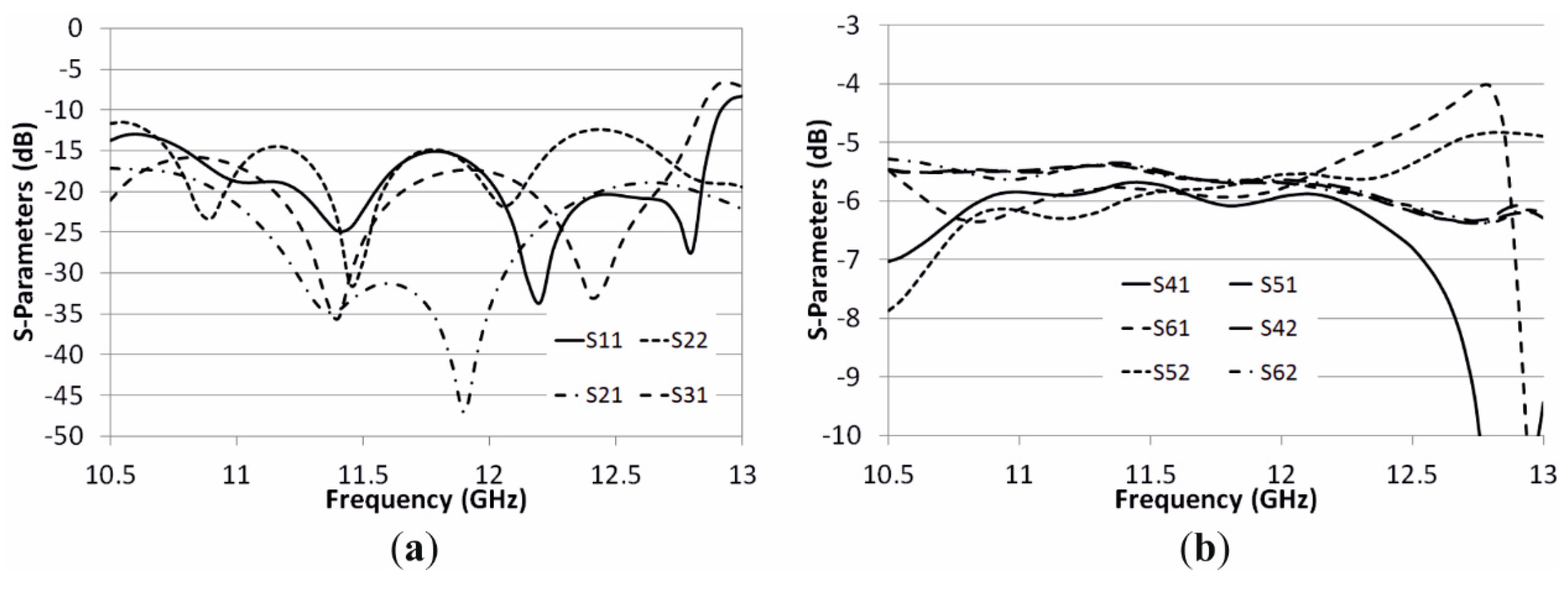
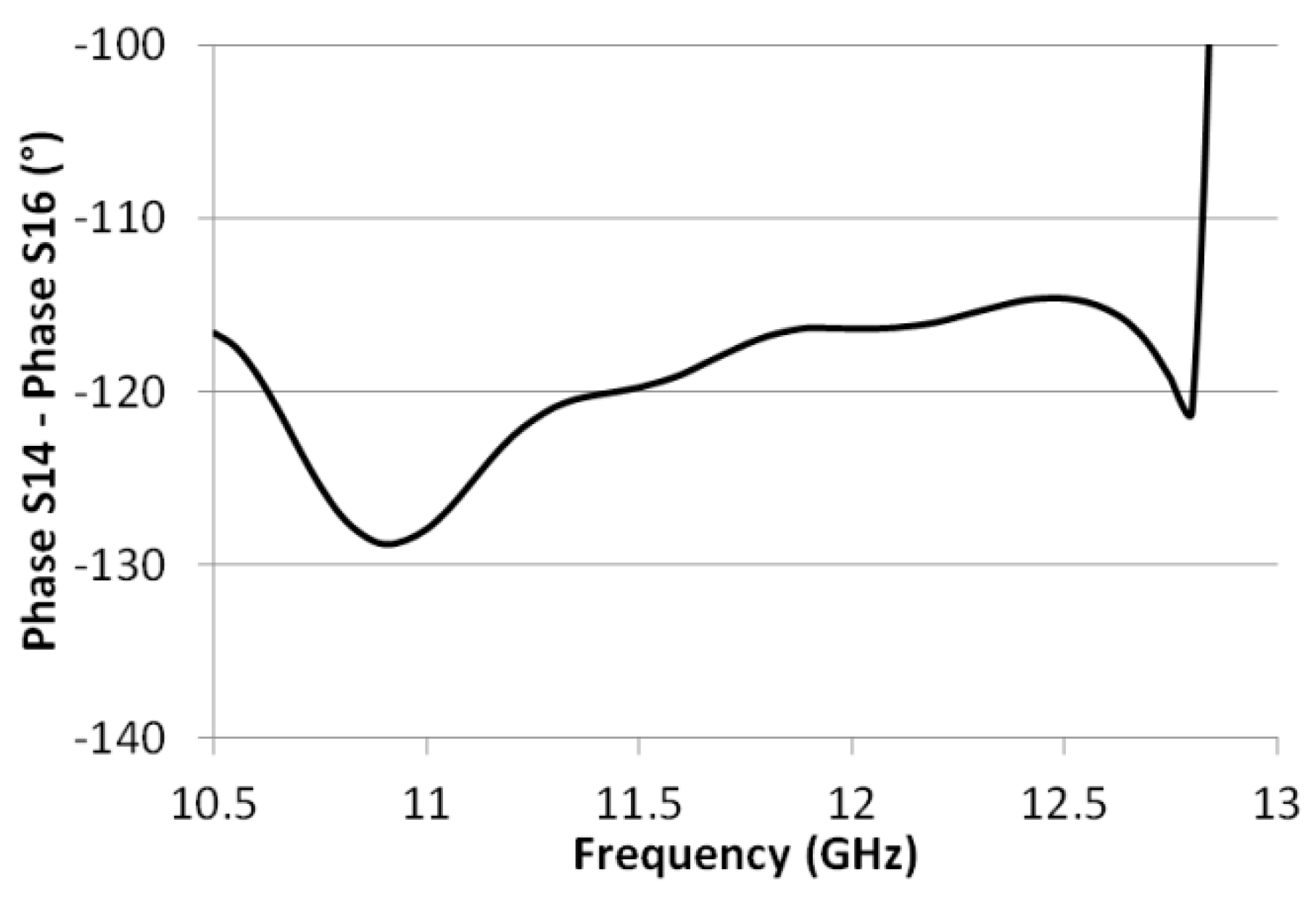
Figure 8a shows the experimental reflection coefficients and the isolation among input ports. Figure 8b shows the experimental transmission coefficients. The experimental phase difference satisfied Equation (6) with a deviation of +5°/−8°, as shown in Figure 9. The return loss can be further improved by adding more steps or irises in the waveguides connecting SMA ports to the core of the device. This approach was used, for example, in [34,35]. However, this increased the final size of the coupler.
3.3. Magic Tee
The Magic Tee is, in practice, a directional coupler with 3 dB coupling, where the signals at the output ports are in opposition of phase. The device can also be used to make the sum and the difference of two input signals, so it is very important for many applications, for example, radars and mixers. The scattering matrix of the ideal Magic Tee follows [43]:
where port 1 is the sum port and port 4 is the difference one.
The standard waveguide Magic Tee is a 3D component, being a combination of an H-plane junction and an E-plane junction [43]. Therefore, it cannot be easily built using a single layer substrate. In the literature there were three different approaches to solve this problem. The first one made use of two different substrates [44,45,46], the second approach consisted of connecting the sum and difference circuits by means of a slotline, and the third approach made use of a phase shifter to adjust the phase of one output [47,48]. In the first case, the device had to be built by attaching together two substrates, using screws for example. This made the device more complicated and expensive. However, the frequency response was usually better in terms of bandwidth and isolation, with respect to single layer implementations.
In [46], a double-layer magic tee was designed starting from the H-plane T junction (Figure 10a). This junction matched well and contained a small slot that was used to connect the difference port fabricated in another board (Figure 10b). The isolation between sum and difference ports was enforced by the different field symmetries when the ports were excited. The two boards were then attached with screws (Figure 11). In the figure, port 1 is the sum port and port 4 is the difference one.
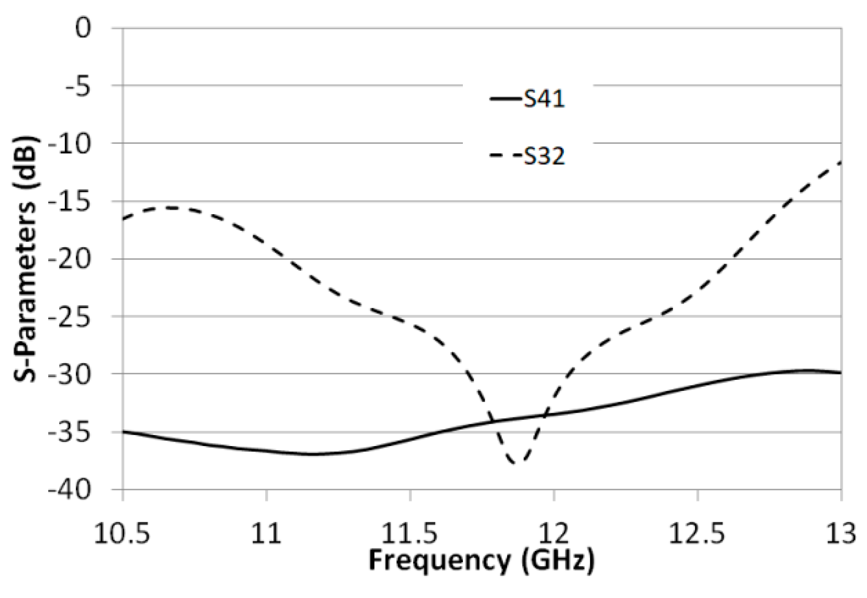
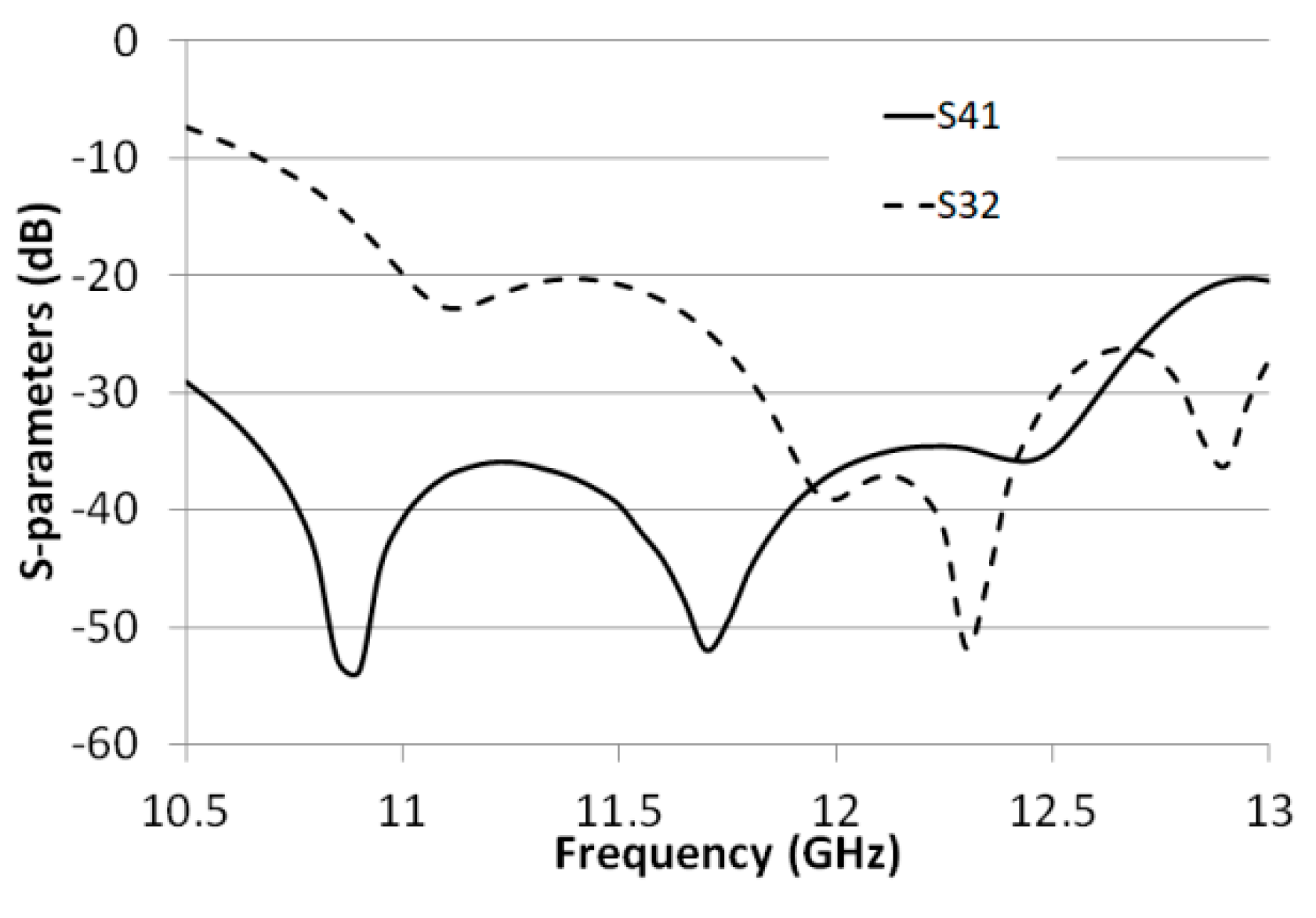
The final size of the device, with the transitions to SMA connectors, was 60 × 60 mm2, whereas the core of the coupler without the connectors was 32 × 25 mm2. Figure 12 shows the experimental reflection and transmission coefficients. With this simple design, a return loss of at least 12 dB can be obtained over the band 10.5 GHz–12.7 GHz. The transmission from the difference port to the output ports (i.e., S24 and S34) was affected by additional losses due to the additional length of the waveguide.
Figure 13 shows the isolation among the ports. As expected, the isolation between the sum and difference (S41) port was higher.
A solution based on the second approach is shown in Figure 14. In this case, the device was built into a single layer, and the H-plane and E-plane junctions were connected by using a slotline between them (Figure 14b).
The device was designed in two steps, using the same method of the double-layer magic tee. First, the H-plane junction was optimized with an aperture to make space for the slotline. This aperture was narrow enough in order to avoid any power leakage when the sum port was excited. Then, the E-plane junction was connected using the slotline. This solution was simpler to build compared to the double-layer one, but had some drawbacks. The slotline was not enclosed, so the device suffered from radiation loss. In this view, we could expect more losses when the field in the slotline was excited, i.e., when the difference port was fed. Moreover, the band was narrower when compared to the double layer implementation. On the other hand, the isolation was very good, especially between the sum and difference ports, because it was enforced by field symmetry. The final size of the device was 70 × 70 mm2, whereas the core without the transitions to SMA connectors was 37 × 37 mm2. Figure 15 shows the experimental reflection and transmission coefficients of the prototype. Figure 16 shows the isolation among ports.
4. Substrate Integrated Waveguide (SIW) Antennas
The use of SIW technology appears to be very interesting in producing low profile, light, and low-cost antennas. However, the design of high gain, squint-less, and very wide band SIW antennas can be quite challenging. There are some methods to achieve this, for example, by using slot arrays [49] or by using cavity-backed patches [50,51,52,53]. In most cases, the performances obtained by SIW antennas are lower compared to their rectangular waveguide counterparts [54,55,56,57,58]. However, substrate integrated waveguides are gaining a lot of attention for their fabrication of low profile and low-cost antennas for 5G applications [59,60], where standard waveguides are not practical. In particular, the gain of the antenna is a trade-off since it increases linearly as the area of the antenna increases, while it decreases exponentially with the length of the transmission lines as a result of losses. In this view, for a given substrate, it is not convenient to make very big antennas because, above a certain size, the gain actually decreases with increasing dimensions. On the other hand, when the radiating slots and the BFN are on the same substrate layer, the crossing between them must be avoided. The radiating elements must be far enough from the discontinuities in order to avoid asymmetries in the radiation pattern. In this view, very good results can be obtained with the example illustrated in the following [61].
Since the band of the antenna was in the interval from 10.7 GHz to 12.7 GHz, the antenna must be squint-less over a very wide range of frequencies. This means that traveling wave antennas cannot be used, since they are affected by the variation of the squint of the main lobe as the frequency changes. Also, resonating subarrays made by several radiating elements cannot be used, since their band is limited.
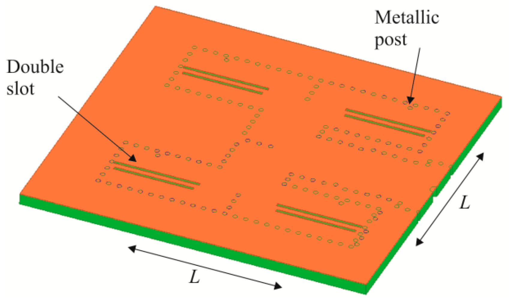
The basic idea to satisfy the specifications was the use of special radiating slots that offered a wideband response that was connected using a SIW BFN. The basic brick of the antenna was the 4 × 2 element shown in Figure 17. The relatively high dielectric permittivity of the Taconic RF-35 substrate was exploited to shrink the network in such a way that the distance between two adjacent slots was less than half the wavelength (in the free space), thus avoiding the grating lobes.
In order to obtain good radiation over a very wide band, the single radiating element was composed of two slots and a cylindrical metallic post (Figure 17). The two radiating slots were called “active” and “passive”. The active slot resonant length depended on the offset with respect to the center of the waveguide [62]. The passive slot was positioned at the center of the waveguide. It could radiate thanks to the active slot and the metallic post, since they perturbed the field inside the SIW. The lengths of the slots were similar, but their resonant frequency was different because of the different offset from the center line [63,64], thus widening the band with respect to the single radiating slot. The position of the small metallic post was then used to enhance the radiation from both slots.
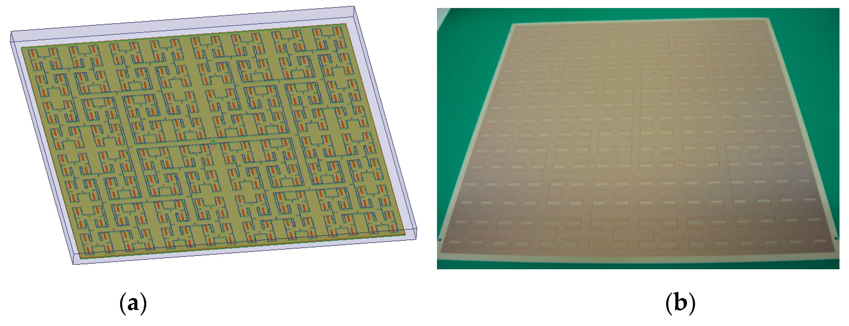
The 4 × 2 arrays were then connected by using a single layer SIW network in order to realize a uniform array, thus generating a broadside main lobe. Figure 18 shows the built array that was composed of 32 × 16 radiating slots. The final size of the antenna was 352 × 352 mm2. The antenna was designed using a standard a commercial simulator (Ansys HFSS) for the SIW network and a home-made software for the external part [65]. The latter takes into account the radiation from all the slots into the free space and the mutual coupling among them.
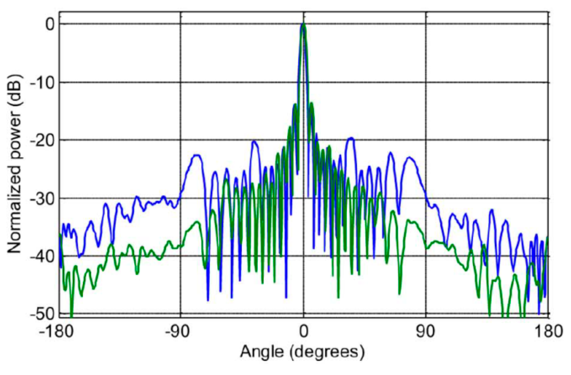
The measured radiation pattern is shown in Figure 19, while the variation of the main lobe with frequency is shown in Figure 20. The results show that the main lobe was almost fixed with the frequency.
The gain of the antenna was 25 dB and it was almost constant from 10.7 GHz to 12.7 GHz. The value was slightly lower than expected from simulations (27 dB), probably because of higher losses than expected in the substrate.
5. New Trends (Empty SIW)
One of the recent trends in SIW technology is the so-called empty substrate integrated waveguide (ESIW) or air-filled SIW [66,67]. In practice, because of the high losses of the dielectric, even when a very expensive one was used, this solution created an empty waveguide inside a PCB in order to reduce losses and maintain the other characteristics of SIWs. There were some attempts to build empty SIWs in the literature. For example, in [68], the structure was made by stacking printed boards between two metallic covers, but this solution was not advantageous over a device made by a machined block of aluminum or copper. In [69], another solution was proposed. However, a part of the EM field was inside a dielectric material, so that the dielectric losses were not negligible and the advantage of the solution was limited. Very recently [70,71,72,73,74,75] other solutions have been proposed, but they used screws to close the final prototype. For example, in [71] a sandwich of three substrates was proposed, where the middle one was machined in order to create the empty waveguide. The upper and lower substrates can be made of low-cost material, such as FR4, whereas the middle layer was made of more expensive material (Rogers RT/duroid 6002®). Moreover, the authors did not specify how the sandwich of layers was glued. Also, many transitions between planar waveguides (i.e., microstrips or coplanar waveguides) and empty SIW have been designed [76,77,78,79,80,81].
The devices obtained by those methods were produced by using different processes, so they were not suitable for mass production. Moreover, the use of screws did not ensure the perfect planarity of the device and increased the size and weight, thus weakening the advantages of SIWs.
In order to overcome these problems, a solution to build empty waveguides embedded in a single dielectric layer has been presented in [82]. With this solution, low loss and low-cost devices can be made, while maintaining the compatibility with standard PCB processes.
The waveguide was built by using a stack of two substrates (Figure 21). The main substrate was thicker (2 mm in this case) and it was milled to build the waveguide. Then, a layer of copper was deposited by using chemical deposition or electroplating, depending on the thickness needed. Of course, the width of the milled waveguide depended on the thickness of the deposited copper in order to obtain the desired cutoff frequency. Above the main substrate a thin layer of substrate (250 um thick), metalized on both sides, was attached by using a no-flow prepreg. The prepreg itself was worked so as to open some apertures of the same size of the waveguides in such a way to avoid the field inside the dielectric and then to reduce losses. This gluing process was done at high pressure and high temperature, and it was exactly the same used in the production of multi-layer PCBs. It is worth noting that the dimensions of the holes in the main substrate and in the prepreg were chosen in a suitable way in order to compensate any variations as a result of the gluing process. This reduced the dielectric inside the waveguides, thus reducing losses and improving the repeatability.
Since the prepreg was non-conductive, there was a discontinuity between the main substrate and the cover. The electrical continuity between lower and upper substrates was then guaranteed by using two rows of metalized via holes along the guide, similar to SIWs (Figure 22).
Looking at Figure 22, it was apparent that the EM field was mostly inside the empty guide with only a minimal part inside the prepreg. Moreover, the field was not inside the dielectric of the main and secondary layers. This means that the substrate used for the device can be a common FR4, which is low cost, rigid, and easy to machine.
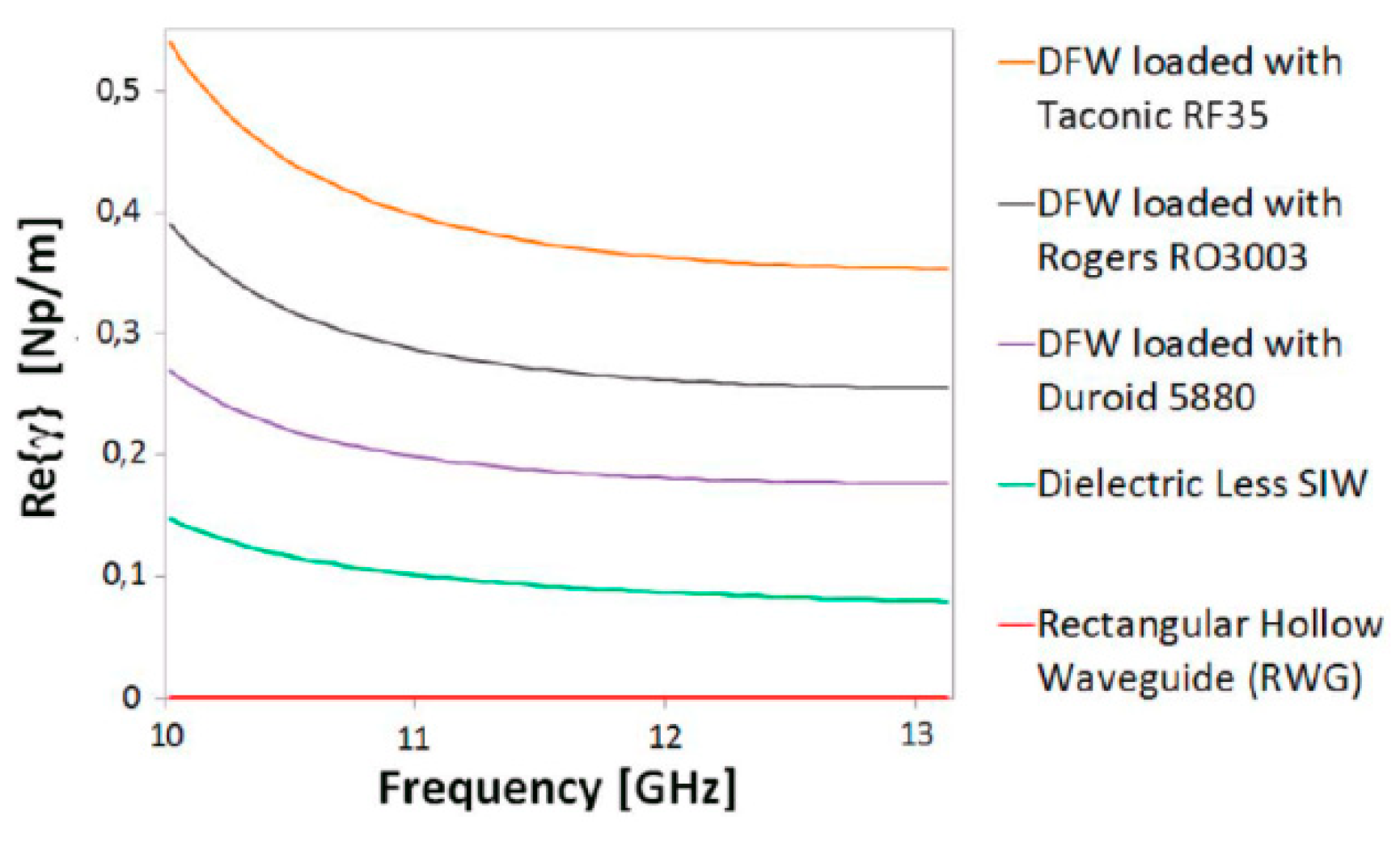
The performances of the waveguide built by this process were very promising, since the losses were lower than SIWs using very expensive substrates, such as Rogers RT/duroid® 5880 or Rogers RO3003™ (Figure 23). In this comparison, the dielectric loaded SIWs were designed so that the TE10 cut-off frequency was the same for all samples. Moreover, the conductor losses were neglected in order to compare only the dielectric losses. The dielectric-absent SIW was simulated using a low-cost material (ITEQ IT-158) with the corresponding prepreg (Tuc TU-84P NF).
It has to be stressed that the use of low-cost substrates compensates for the complexity of the process, thus, the cost of the device is very low.
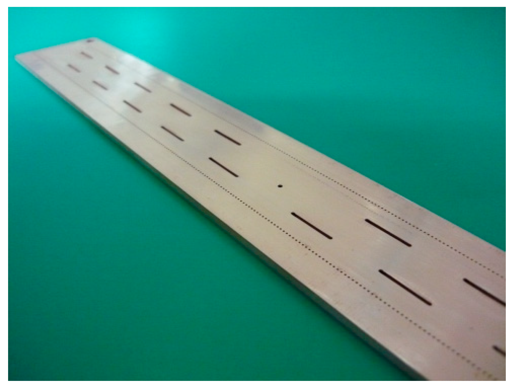
Using this technology, a resonant slotted array was also built (Figure 24). The antenna was composed of 20 slots, each 12.82 mm in length that corresponded to a resonant frequency of 11.75 GHz. The spacing of the slots was 25.64 mm, nearly λg/2 in the dielectric-absent SIW, and the antenna was fed by an SMA connector placed in the middle of the array. The experimental results were in very good agreement with simulations (Figure 25). The 15 dB bandwidth around 11.75 GHz was 100 MHz (0.85%), and the half power beam width was nearly 8°. These results showed that the process can be used for the fabrication of microwave components.
6. Conclusions
A review of some SIW components designed for DVB-S applications has been presented. The main goals of the proposed solutions have been the cost of the devices, which should be as low as possible, and the size of the devices, which should be as small as possible. The first goal has been satisfied by using a Taconic RF-35 substrate.
Despite those constraints, the performances obtained by the synthesized devices are very good, and some improvements to the proposed solutions have been also illustrated.
The proposed devices can be easily modified to work at other frequencies by simply shrinking or enlarging them. As very general-purpose devices, they also can be used for other applications.
Author Contributions
Conceptualization, investigation, and methodology, G.V., D.M., A.M., M.F., F.P.; writing—original draft preparation, G.V.; writing—review and editing, D.M., A.M., M.F. and F.P.; supervision, F.P.; project administration, F.P.; funding acquisition, A.M., M.F, F.P.
Funding
This research was funded by the Italian Ministry of University (MIUR), grant number PON01_01224 on development of Substrate Integrated Waveguide circuits for ITC applications.
Acknowledgments
The prototypes shown in this review were built by Somacis S.p.A., Via Jesina, 60022 Castelfidardo (AN), Italy. Author would like to thank Dr. Francesco Bigelli for the realization of the empty substrate integrated waveguide prototypes.
Conflicts of Interest
The authors declare no conflict of interest. The funders had no role in the design of the study; in the collection, analyses, or interpretation of data; in the writing of the manuscript, or in the decision to publish the results.
References
- Deslandes, D.; Wu, K. Integrated microstrip and rectangular waveguide in planar form. IEEE Microw. Wirel. Compon. Lett. 2001, 11, 68–70. [Google Scholar] [CrossRef]
- Deslandes, D.; Wu, K. Single-substrate integration technique for planar circuits and waveguide filters. IEEE Trans. Microw. Theory Tech. 2003, 51, 593–596. [Google Scholar] [CrossRef]
- Deslandes, D.; Wu, K. Accurate modelling, wave mechanism and design considerations of a substrate integrated waveguide. IEEE Trans. Microw. Theory Tech. 2006, 54, 2516–2526. [Google Scholar] [CrossRef]
- Bozzi, M.; Georgiadis, A.; Wu, K. Review of substrate-integrated waveguide circuits and antennas. IET Microw. Antennas Propag. 2011, 5, 909–920. [Google Scholar] [CrossRef]
- Zheludev, N.I.; Kivshar, Y.S. From metamaterials to metadevices. Nat. Mater. 2012, 11, 917–924. [Google Scholar] [CrossRef] [PubMed]
- La Spada, L.; Bilotti, F.; Vegni, L. Metamaterial resonator arrays for organic and inorganic compound sensing. In Proceedings of the Photonics, Devices and System V, Prague, Czech Republic, 24–26 August 2011. [Google Scholar]
- Liberal, I.; Engheta, N. Near-zero refractive index photonics. Nat. Photonics 2017, 11, 149–158. [Google Scholar] [CrossRef]
- La Spada, L. Metasurfaces for Advanced Sensing and Diagnostic. Sensors 2019, 19, 355. [Google Scholar] [CrossRef] [PubMed]
- Soavi, G.; Wang, G.; Rostami, H.; Purdie, D.G.; De Fazio, D.; Ma, T.; Luo, B.; Wang, J.; Ott, A.K.; Yoon, D.; et al. Broadband, electrically tunable third-harmonic generation in graphene. Nat. Nanotechnol. 2018, 13, 583–588. [Google Scholar] [CrossRef] [PubMed]
- Mamalis, A.G.; Kladas, A.; Enokizono, M. Spectral Green’s Function for SPR Meta-Structures. Mater. Sci. Forum 2014, 792, 110–114. [Google Scholar]
- Han, L.; Wu, K.; Chen, X.P.; He, F. Accurate and efficient design technique for wideband substrate integrated waveguide directional couplers. Int. J. RF Microw. Comput.-Aided Eng. 2011, 22, 48–59. [Google Scholar] [CrossRef]
- Bozzi, M.; Xu, F.; Deslandes, D.; Wu, K. Modeling and design considerations for substrate integrated waveguide circuits and components. In Proceedings of the 8th International Conference on Telecommunications in Modern Satellite, Cable and Broadcasting Services (TELSIKS 2007), Nis, Serbia & Montenegro, 26–28 September 2007. [Google Scholar]
- Cassivi, Y.; Perregrini, L.; Arcioni, P.; Bressan, M.; Wu, K.; Conciauro, G. Dispersion characteristics of substrate integrated rectangular waveguide. IEEE Microw. Wirel. Compon. Lett. 2002, 12, 333–335. [Google Scholar] [CrossRef]
- Xu, F.; Wu, K. Guided–wave and leakage characteristics of substrate integrated waveguide. IEEE Trans. Microw. Theory Tech. 2005, 53, 66–73. [Google Scholar]
- Salehi, M.; Mehrshahi, E. A closed–from formula for dispersion characteristics of fundamental SIW mode. IEEE Microw. Wirel. Compon. Lett. 2011, 21, 4–6. [Google Scholar] [CrossRef]
- Kordiboroujeni, Z.; Bornemann, J. Designing the width of substrate integrated waveguide structures. IEEE Microw. Wirel. Compon. Lett. 2013, 23, 518–520. [Google Scholar] [CrossRef]
- Xu, F.; Zhang, Y.; Hong, W.; Wu, K.; Cui, T.J. Finite difference frequency-domain algorithm for modeling guided wave properties of substrate integrated waveguide. IEEE Trans. Microw. Theory Tech. 2003, 51, 2221–2227. [Google Scholar]
- Bozzi, M.; Pasian, M.; Perregrini, L.; Wu, K. Modeling of conductor, dielectric, and radiation losses in substrate integrated waveguide by the boundary integral–resonant mode expansion method. IEEE Trans. Microw. Theory Tech. 2008, 56, 3153–3161. [Google Scholar] [CrossRef]
- Hao, Z.C.; Hong, W.; Chen, J.X.; Zhou, H.X.; Wu, K. Single-layer substrate integrated waveguide directional couplers. IEEE Proc. Microw. Antennas Propag. 2006, 153, 426–431. [Google Scholar] [CrossRef]
- Bing, L.; Hong, W.; Hao, Z.C.; Wu, K. Substrate integrated waveguide 180-degree narrow wall directional coupler. In Proceedings of the IEEE APMC Proceedings, Suzhou, China, 4–7 December 2005. [Google Scholar]
- Liu, B.; Hong, W.; Zhang, Y.; Chen, J.X.; Wu, K. Half-mode substrate integrated waveguide (HMSIW) double-slot coupler. Electron. Lett. 2007, 43, 113–114. [Google Scholar] [CrossRef]
- Ali, A.; Coccetti, F.; Aubert, H.; Fonseca, N.J.G. Novel multi-layer SIW broadband coupler for nolen matrix design in Ku band. In Proceedings of the IEEE/MTT-S International Microwave Symposium, San Diego, CA, USA, 5–11 July 2008. [Google Scholar]
- Labay, V.A.; Bornemann, J. E-plane directional couplers in substrate-integrated waveguide technology. In Proceedings of the Asia-Pacific Microwave Conference (APMC 2008), Macau, China, 16–20 December 2008. [Google Scholar]
- Labay, V.A.; Bornemann, J. Design of dual-band substrate-integrated waveguide E-plane directional couplers. In Proceedings of the Asia Pacific Microwave Conference (APMC 2009), Singapore, 7–10 December 2009; pp. 2116–2119. [Google Scholar]
- Navarro, D.V.; Carrera, L.F.; Baquero-Escudero, M.; Rodrigo-Penarrocha, V.M. Compact substrate integrated waveguide directional couplers in Ku and K bands. In Proceedings of the 40th European Microwave Conference, Paris, France, 28–30 September 2010; pp. 1178–1181. [Google Scholar]
- Ali, A.A.M.; El-Shaarawy, H.B.; Aubert, H. Compact wideband double-layer half-mode substrate integrated waveguide 90° coupler. Electron. Lett. 2011, 47, 598–599. [Google Scholar] [CrossRef]
- Riblet, H. The short-slot hybrid junction. Proc. IRE 1952, 40, 180–184. [Google Scholar] [CrossRef]
- Castellano, T.; Losito, O.; Mescia, L.; Chiapperino, M.A.; Venanzoni, G.; Mencarelli, D.; Angeloni, G.; Renghini, C.; Carta, P.; Potenza, P.; et al. Substrate integrated waveguide fixed phase shifter for 90-degree directional coupler. In Proceedings of the IEEE Proceeding International Conference on Microwaves, Communications, Antennas and Electronic Systems (COMCAS 2013), Tel Aviv, Israel, 21–23 October 2013. [Google Scholar]
- Castellano, T.; Losito, O.; Mescia, L.; Chiapperino, M.A.; Venanzoni, G.; Mencarelli, D.; Angeloni, G.; Renghini, C.; Carta, P.; Prudenzano, F. Feasibility Investigation of Low Cost Substrate Integrated Waveguide (SIW) Directional Couplers. Prog. Electromagn. Res. B 2014, 59, 31–44. [Google Scholar] [CrossRef]
- Yan, L.; Hong, W. Investigations on the propagation characteristics of the substrate integrated waveguide based on the method of lines. IEE Proc. Microw. Antennas Propag. 2005, 152, 35–42. [Google Scholar] [CrossRef]
- Hao, Z.C.; Hong, W.; Chen, J.X.; Chen, X.P.; Wu, K. Planar diplexer for microwave integrated circuits. IEEE Proc. Microw. Antennas Propag. 2005, 152, 455–459. [Google Scholar] [CrossRef]
- Venanzoni, G.; Mencarelli, D.; Morini, A.; Farina, M.; Angeloni, G.; Renghini, C.; Carta, P.; Potenza, P.; Losito, O.; Mescia, L.; et al. Single-Layer Standalone Wideband Substrate-integrated Waveguide Directional Coupler. Microw. Opt. Technol. Lett. 2014, 56, 1141–1144. [Google Scholar] [CrossRef]
- Morini, A.; Farina, M.; Cellini, C.; Rozzi, T.; Venanzoni, G. Design of low-cost non-radiative SMA-SIW Launchers. In Proceedings of the European Microwave Conference, Manchester, UK, 10–15 September 2006. [Google Scholar]
- Alessandri, F.; Giordano, M.; Guglielmi, M.; Martirano, G.; Vitulli, F. A new multiple-tuned six-port riblet-type directional coupler in rectangular waveguide. IEEE Trans. Microw. Theory Tech. 2003, 51, 1441–1448. [Google Scholar] [CrossRef]
- Salehi, M.; Bornemann, J.; Mehrshahi, E. Wideband Substrate-Integrated Waveguide Six-Port Power Divider/Combiner. Microw. Opt. Technol. Lett. 2013, 55, 2984–2986. [Google Scholar] [CrossRef]
- Venanzoni, G.; Mencarelli, D.; Morini, A.; Farina, M.; Losito, O.; Prudenzano, F. Compact Substrate Integrated Waveguide Six-Port Directional Coupler for X-Band Applications. Microw. Opt. Technol. Lett. 2015, 57, 2589–2592. [Google Scholar] [CrossRef]
- Xu, X.; Bosisio, R.G.; Wu, K. A new six-port junction based on substrate integrated waveguide technology. IEEE Trans. Microw. Theory Tech. 2005, 53, 2267–2273. [Google Scholar]
- Djerafi, T.; Daigle, M.; Boutayeb, H.; Zhang, X.; Wu, K. Substrate integrated waveguide six-port broadband front-end circuit for millimeter-wave radio and radar systems. In Proceedings of the 39th European Microwave Conference, Rome, Italy, 28 September–2 October 2009; pp. 77–80. [Google Scholar]
- Doghri, A.; Djerafi, T.; Ghiotto, A.; Wu, K. Broadband substrate integrated- waveguide six-port applied to the development of polarimetric imaging radiometer. In Proceedings of the 41st European Microwave Conference (EuMA), Manchester, UK, 10–13 October 2011; pp. 393–396. [Google Scholar]
- Dusek, M.; Sebesta, J. Design of substrate integrated waveguide six-port for 3.2 GHz modulator. In Proceedings of the 34th International Conference on Telecommunications Signal Processing (TSP), Budapest, Hungary, 18–20 August 2011; pp. 274–278. [Google Scholar]
- Wu, L.-N.; Zhang, X.-C.; Tong, C.-M.; Zhou, M. A new substrate integrated waveguide six-port circuit. In Proceedings of the IEEE International Conference on Microwave and Millimeter Wave Technology (ICMMT), Chengdu, China, 8–11 May 2010; pp. 59–61. [Google Scholar]
- Chen, J.X.; Hong, W.; Tang, H.J.; Yan, P.P.; Liu, B.; Wu, K. A millimeter wave six-port network using half-mode substrate integrated waveguide. J. Infrared Millim. Terahertz Waves 2012, 33, 348–356. [Google Scholar] [CrossRef]
- Pozar, D.M. Microwave Engineering, 3rd ed.; Wiley: Hoboken, NJ, USA, 2004. [Google Scholar]
- Liu, M.; Feng, Z. A novel hybrid planar SIW magic Tee and monopulse antenna. Microw. Opt. Technol. Lett. 2010, 52, 686–689. [Google Scholar] [CrossRef]
- Aram, I.; Garb, K.; Kastner, R. Design of E-plane T-junction dividers using substrate integrated waveguide (SIW). In Proceedings of the 28th IEEE Convention of Electrical and Electronics Engineers, Eilat, Israel, 3–5 December 2014. [Google Scholar]
- Venanzoni, G.; Mencarelli, D.; Morini, A.; Farina, M.; Losito, O.; Prudenzano, F. Compact Double-Layer Substrate Integrated Waveguide Magic Tee For X-Band Applications. Microw. Opt. Technol. Lett. 2016, 58, 932–936. [Google Scholar] [CrossRef]
- Cheng, Y.; Hong, W.; Wu, K. Novel Substrate Integrated Waveguide fixed phase shifter for 180-degree Directional Coupler. In Proceedings of the IEEE/MTT-S International Microwave Symposium, Honolulu, HI, USA, 3–8 June 2007; pp. 189–192. [Google Scholar]
- Liu, B.; Hong, W.; Zhang, Y.; Tang, H.J.; Yin, X.; Wu, K. Half Mode Substrate Integrated Waveguide 180° 3-dB Directional Couplers. IEEE Trans. Microw. Theory Tech. 2007, 55, 2586–2592. [Google Scholar]
- Wan, L.; Hong, W.; Hua, C.; Chen, J.; Wu, K. Simulation and experiment on siw slot array antennas. IEEE Microw. Wirel. Compon. Lett. 2004, 14, 446–448. [Google Scholar]
- Awida, M.H.; Fathy, A.E. Substrate-integrated waveguide Ku-band cavity-backed microstrip patch array antenna. IEEE Antennas Wirel. Propag. Lett. 2009, 8, 1054–1056. [Google Scholar] [CrossRef]
- Losito, O.; Mescia, L.; Mencarelli, D.; Venanzoni, G.; Prudenzano, F. SIW Cavity-Backed Patch Antenna for Ku Band Applications. In Proceedings of the 7th European Conference on Antennas and Propagation (EUCAP 2013), Gothenburg, Sweden, 8–12 April 2013; pp. 3095–3098. [Google Scholar]
- Losito, O.; Mescia, L.; Chiapperino, M.A.; Castellano, T.; Venanzoni, G.; Mencarelli, D.; Angeloni, G.; Carta, P.; Starace, E.M.; Prudenzano, F. X-Band SIW Cavity-Backed Patch Antenna for Radar Applications. In Proceedings of the 43rd European Microwave Conference, Nuremberg, Germany, 6–11 October 2013; pp. 199–202. [Google Scholar]
- Zhang, T.; Hong, W.; Zhang, Y.; Wu, K. Design and analysis of SIW cavity backed dual-band antennas with a dual-mode triangular-ring slot. IEEE Trans. Antennas Propag. 2014, 62, 5007–5016. [Google Scholar] [CrossRef]
- Jin, L.; Lee, R.M.; Robertson, I.D. Design and performance of log-periodic substrate integrated waveguide slot antennas. In Proceedings of the IEEE MTT-S International Microwave Symposium Digest, Montreal, QC, Canada, 17–22 June 2012. [Google Scholar]
- Liu, W.; Chen, Z.N.; See, T.S.P.; Liu, F. SIW-slot-fed thin beam-squint-free Fabry-Pérot cavity antenna with low backlobe levels. IEEE Antennas Wirel. Propag. Lett. 2014, 13, 552–554. [Google Scholar] [CrossRef]
- Cho, D.; Lee, H.-Y. Folded corrugated SIW (FCSIW) slot antenna for backlobe suppression. IEEE Antennas Wirel. Propag. Lett. 2013, 12, 1276–1279. [Google Scholar] [CrossRef]
- Xu, J.; Chen, Z.N.; Qing, X. CPW center-fed single-layer SIW slot antenna array for automotive radars. IEEE Trans. Antennas Propag. 2014, 62, 4528–4536. [Google Scholar] [CrossRef]
- Mbaye, M.; Hautcoeur, J.; Talbi, L.; Hettak, K. Bandwidth broadening of dual-slot antenna using substrate integrated waveguide (SIW). IEEE Antennas Wirel. Propag. Lett. 2013, 12, 1169–1171. [Google Scholar] [CrossRef]
- Li, Y.; Luk, K.M. Low-Cost High-Gain and Broadband Substrate-Integrated-Waveguide-Fed Patch Antenna Array for 60-GHz Band. IEEE Trans. Antennas Propag. 2014, 62, 5531–5538. [Google Scholar] [CrossRef]
- Zhu, Q.; Ng, K.B.; Chan, C.H.; Luk, K.M. Substrate-Integrated-Waveguide-Fed Array Antenna Covering 57–71 GHz Band for 5G Applications. IEEE Trans. Antennas Propag. 2017, 65, 6298–6306. [Google Scholar] [CrossRef]
- Mencarelli, D.; Morini, A.; Prudenzano, F.; Venanzoni, G.; Bigelli, F.; Losito, O.; Farina, M. Broadband Single-Layer Slotted Array Antenna in SIW Technology. IEEE Antennas Wirel. Propag. Lett. 2016, 15, 263–265. [Google Scholar] [CrossRef]
- Elliot, R. Antenna Theory and Design; Series Electromagnetic Wave Theory; IEEE Press: Piscataway, NJ, USA, 2003. [Google Scholar]
- Josefsson, L. Analysis of longitudinal slots in rectangular waveguides. IEEE Trans. Antenna Propag. 1987, AP-35, 1351–1357. [Google Scholar] [CrossRef]
- Rengarajan, S.R.; Steinbeck, M. Longitudinal slots in dielectric filled rectangular waveguides. In Proceedings of the Antennas and Propagation Society Symposium 1991 Digest, London, ON, Canada, 24–28 June1991; Volume 2, pp. 1276–1279. [Google Scholar]
- Morini, A.; Rozzi, T.; Venanzoni, G. On the analysis of slotted waveguide arrays. IEEE Trans. Antennas Propag. 2006, 54, 2016–2021. [Google Scholar] [CrossRef]
- Ranjkesk, N.; Shahabadi, M. Reduction of dielectric losses in substrate integrated waveguide. Electron. Lett. 2006, 42, 1230–1231. [Google Scholar] [CrossRef]
- Belenguer, A.; Esteban, H.; Borja, A.L.; Boria, V.E. Empty SIW Technologies. IEEE Micow. Mag. 2019, 20, 24–45. [Google Scholar] [CrossRef]
- Mohammadi, P. Low Loss Substrate Integrated Waveguide N-Way Power Divider. Ph.D. Dissertation, Department of Electrical and Electronic Engineering, Middle East Technical University, Ankara, Turkey, 2012. [Google Scholar]
- Jin, L.; Lee, R.M.A.; Robertson, I. Analysis and design of a novel low-loss hollow substrate integrated waveguide. IEEE Trans. Microw. Theory Tech. 2014, 62, 1616–1624. [Google Scholar] [CrossRef]
- Belenguer, A.; Esteban, H.; Boria, V. Novel empty substrate integrated waveguide for high-performance microwave integrated circuits. IEEE Trans. Microw. Theory Tech. 2014, 62, 832–839. [Google Scholar] [CrossRef]
- Parment, F.; Ghiotto, A.; Vuong, T.P.; Duchamp, J.M.; Wu, K. Air-Filled Substrate Integrated Waveguide for Low-Loss and High Power-Handling Millimeter-Wave Substrate Integrated Circuits. IEEE Trans. Microw. Theory Tech. 2015, 63, 1228–1238. [Google Scholar] [CrossRef]
- Quiles, F.; Belenguer, A.; Martinez, J.A.; Nova, V.; Esteban, H.; Boria, V. Compact Microstrip to Empty Substrate-Integrated Coaxial Line Transition. IEEE Microw. Wirel. Compon. Lett. 2018, 28, 1080–1082. [Google Scholar] [CrossRef]
- Fernandez, M.D.; Ballesteros, J.A. Design of a hybrid directional coupler in empty substrate integrated waveguide (ESIW). IEEE Microw. Wirel. Compon. Lett. 2015, 25, 796–798. [Google Scholar] [CrossRef]
- Parment, F.; Ghiotto, A.; Vuong, T.P.; Duchamp, J.M.; Wu, K. Low-loss air-filled substrate integrated waveguide (SIW) band-pass filter with inductive posts. In Proceedings of the 45th European Microwave Conference (EuMC), Paris, France, 7–10 September 2015. [Google Scholar]
- Martinez, L.; Martinez, J.A.; Borja, A.L.; Esteban, H.; Boria, V.E.; Belenguer, A. Compact Bandpass Filter in Empty Substrate Integrated Coaxial Line. In Proceedings of the 48th European Microwave Conference (EuMC), Madrid, Spain, 25–27 September 2018; pp. 162–165. [Google Scholar]
- Parment, F.; Ghiotto, A.; Vuong, T.P.; Duchamp, J.M.; Wu, K. Broadband transition from dielectric-filled to air-filled substrate integrated waveguide for low loss and high power handling millimeter-wave substrate integrated. In Proceedings of the IEEE MTT-S International Microwave Symposium (IMS 2014), Tampa, FL, USA, 1–6 June 2014. [Google Scholar]
- Belenguer, A.; Borja, A.L.; Esteban, H.; Boria, V.E. High-performance coplanar waveguide to empty substrate integrated coaxial line transition. IEEE Trans. Microw. Theory Tech. 2015, 63, 4027–4034. [Google Scholar] [CrossRef]
- Peng, H.; Xia, X.; Dong, J.; Yang, T. An improved broadband transition between microstrip and empty substrate integrated waveguide. Microw. Opt. Technol. Lett. 2016, 58, 2227–2231. [Google Scholar] [CrossRef]
- Morro, J.V.; Rodriguez, A.; Belenguer, A.; Esteban, H.; Boria, V. Multilevel transition in empty substrate integrated waveguide. Electron. Lett. 2016, 52, 1543–1544. [Google Scholar] [CrossRef]
- Esteban, H.; Belenguer, A.; Sanchez, J.R.; Bachiller, C.; Boria, V.E. Improved low reflection transition from microstrip line to empty substrate-integrated waveguide. IEEE Microw. Wirel. Compon. Lett. 2017, 27, 685–687. [Google Scholar] [CrossRef]
- Khan, Z.U.; Jilani, S.F.; Belenguer, A.; Loh T., H.; Alomainy, A. Empty Substrate Integrated Waveguide-Fed MMW Aperture-Coupled Patch Antenna for 5G Applications. In Proceedings of the 12th European Conference on Antennas and Propagation, London, UK, 9–13 April 2018. [Google Scholar]
- Bigelli, F.; Mencarelli, D.; Farina, M.; Venanzoni, G.; Scalmati, P.; Renghini, C.; Morini, A. Design and Fabrication of a Dielectricless Substrate-Integrated Waveguide. IEEE Trans. Compon. Packag. Manuf. Technol. 2016, 6, 256–261. [Google Scholar] [CrossRef]
Figure 1.
Sketch of a substrate integrated waveguide (SIW).

Figure 2.
Examples of a four-port directional coupler designed in [29]. (a) Coupler #6; (b) Coupler #7, (c) Coupler #8; and (d) Photographs of the prototypes. Figures adapted from [28,29].

Figure 3.
Experimental responses for the couplers shown in Figure 2 [29]. (a) Coupler #6; (b) Coupler #7; and (c) Coupler #8. Figures adapted from [28,29].

Figure 4.
Four-port directional coupler. (a) Sketch of the coupler; (b) Photograph of the coupler. Figures adapted from [32].
Figure 4.
Four-port directional coupler. (a) Sketch of the coupler; (b) Photograph of the coupler. Figures adapted from [32].

Figure 5.
Comparison between simulated and experimental responses of the coupler in Figure 4. (a) Reflection coefficient and isolation; (b) Transmission coefficients. Figures adapted from [32].

Figure 6.
Experimental phase difference between the coupled and direct port of the directional coupler in Figure 4. Figures adapted from [32].

Figure 7.
Photograph of the prototype of the six-port coupler. Figure adapted from [36].
Figure 7.
Photograph of the prototype of the six-port coupler. Figure adapted from [36].

Figure 8.
Experimental response of the six-port coupler shown in Figure 7. (a) Reflection coefficients and isolation among input ports; (b) Transmission coefficients. Figures adapted from [36].

Figure 9.
Experimental phase difference between the output signal on port 4 and 6 when port 1 is fed.
Figure 9.
Experimental phase difference between the output signal on port 4 and 6 when port 1 is fed.

Figure 10.
Layers of the Magic Tee: (a) First layer with the H-plane T-junction; (b) Second layer with the E-plane junction.
Figure 10.
Layers of the Magic Tee: (a) First layer with the H-plane T-junction; (b) Second layer with the E-plane junction.

Figure 11.
Assembled double-layer Magic tee.

Figure 12.
Experimental response of the Magic Tee prototype shown in Figure 11. (a) Reflection coefficients; (b) Transmission coefficients.
Figure 12.
Experimental response of the Magic Tee prototype shown in Figure 11. (a) Reflection coefficients; (b) Transmission coefficients.

Figure 13.
Experimental isolation of the Magic Tee prototype shown in Figure 11.
Figure 13.
Experimental isolation of the Magic Tee prototype shown in Figure 11.

Figure 14.
Single-layer Magic Tee prototype. (a) top view; (b) bottom view.

Figure 15.
Experimental response of the single-layer Magic Tee prototype shown in Figure 14. (a) Reflection coefficients; (b) Transmission coefficients.
Figure 15.
Experimental response of the single-layer Magic Tee prototype shown in Figure 14. (a) Reflection coefficients; (b) Transmission coefficients.

Figure 16.
Experimental isolation of the single-layer Magic Tee prototype shown in Figure 14.
Figure 16.
Experimental isolation of the single-layer Magic Tee prototype shown in Figure 14.

Figure 17.
Basic 4 × 2 antenna block in SIW technology.

Figure 18.
SIW array prototype: (a) Sketch of the prototype; (b) Photograph of the prototype.

Figure 19.
Measured radiation pattern of the antenna shown in Figure 18 [61]: E-plane (blue line); H-plane (green line).

Figure 20.
Squint of the main lobe of the antenna shown in Figure 18 as a function of the frequency [61]: (a) E-plane; (b) H-plane.

Figure 21.
Stack of layers for the integrated empty substrate. FR4 substrates (green), Prepreg (dark red), and copper (orange).
Figure 21.
Stack of layers for the integrated empty substrate. FR4 substrates (green), Prepreg (dark red), and copper (orange).

Figure 22.
Section of the empty SIW. FR4 substrates (green), Prepreg (dark red), and copper (orange).
Figure 22.
Section of the empty SIW. FR4 substrates (green), Prepreg (dark red), and copper (orange).

Figure 23.
Comparison of the losses due to the dielectric in SIW structures with different substrates and the proposed empty SIW [82]. Conductor losses are neglected.
Figure 23.
Comparison of the losses due to the dielectric in SIW structures with different substrates and the proposed empty SIW [82]. Conductor losses are neglected.

Figure 24.
Antenna prototype built with the empty SIW [82].
Figure 24.
Antenna prototype built with the empty SIW [82].

Figure 25.
Comparison between simulated and experimental results for the dielectric-absent antenna [82]. (a) reflection coefficient; (b) radiation pattern.
Figure 25.
Comparison between simulated and experimental results for the dielectric-absent antenna [82]. (a) reflection coefficient; (b) radiation pattern.

© 2019 by the authors. Licensee MDPI, Basel, Switzerland. This article is an open access article distributed under the terms and conditions of the Creative Commons Attribution (CC BY) license (http://creativecommons.org/licenses/by/4.0/).
Share and Cite
MDPI and ACS Style
Venanzoni, G.; Mencarelli, D.; Morini, A.; Farina, M.; Prudenzano, F. Review of Substrate Integrated Waveguide Circuits for Beam-Forming Networks Working in X-Band. Appl. Sci. 2019, 9, 1003. https://doi.org/10.3390/app9051003
AMA Style
Venanzoni G, Mencarelli D, Morini A, Farina M, Prudenzano F. Review of Substrate Integrated Waveguide Circuits for Beam-Forming Networks Working in X-Band. Applied Sciences. 2019; 9(5):1003. https://doi.org/10.3390/app9051003
Chicago/Turabian StyleVenanzoni, Giuseppe, Davide Mencarelli, Antonio Morini, Marco Farina, and Francesco Prudenzano. 2019. "Review of Substrate Integrated Waveguide Circuits for Beam-Forming Networks Working in X-Band" Applied Sciences 9, no. 5: 1003. https://doi.org/10.3390/app9051003
Note that from the first issue of 2016, this journal uses article numbers instead of page numbers. See further details here.