A Novel Magnetic Coupling for Miniaturized Bandpass Filters in Embedded Coaxial SIW


1
iTEAM, Universitat Politècnica de València (UPV), 46022 Valencia, Spain
2
I3M, Universitat Politècnica de València (UPV), 46022 Valencia, Spain
*
Author to whom correspondence should be addressed.
Appl. Sci. 2019, 9(3), 394; https://doi.org/10.3390/app9030394
Submission received: 20 December 2018
/
Revised: 16 January 2019
/
Accepted: 21 January 2019
/
Published: 24 January 2019
(This article belongs to the Special Issue Substrate Integrated Waveguide (SIW) and Its Applications)
Abstract
:In this paper, embedded coaxial substrate integrated waveguide (CSIW) filters with innovative magnetic couplings are presented and studied. By creating the loading capacitance of a combline topology using inner layers of a low-temperature co-fired ceramic (LTCC) stack-up, it is possible to achieve resonator miniaturization while improving the spurious-free band and providing full-packaged solutions. Moreover, a new magnetic coupling scheme consisting of short-ended stripline probes is proposed and analyzed in detail, both for direct and external couplings. An in-line three-pole filter at L-band is designed, manufactured, and measured proving how the proposed approach can be used for designing wideband bandpass filter (BPF) with extremely compact size. The designed BPF is centered at 1.5 GHz with fractional bandwidth (FBW), while the layout size is just mm. The experimental results validate the coaxial SIW technology that allows for, at the same time, easy integration, compact size, flexible design, and enhanced stop-band performance.
1. Introduction
Presently, substrate integrated waveguide (SIW) technology is considered to be a fruitful approach for the design and implementation of microwave and mm-wave components, such as cavity filters, antennas, directional couplers, oscillators, or power amplifiers among others [1]. The fusion of planar and non-planar structures enabled by SIW technology presents an optimal compromise in terms of EM performance, cost, size, and manufacturability. Indeed, moderate-to-high quality factor (Q), excellent planar integration, low weight, and low-cost manufacturing processes in printed circuit board (PCB) and LTCC technology are some of the key advantages that can be obtained conveniently in SIW technology.
Nevertheless, wireless communication systems are imposing increasingly stringent requirements for the performance of microwave filters to be employed for the next-generation wireless and mobile applications. In this context, compactness represents a crucial feature to be addressed in the future microwave BPFs, and for this reason, considerable effort has been recently deployed to increase the miniaturization of SIW filters whose footprint is considered to be still rather large.
As is well known, the combline topology, which can be modeled as a TEM-mode transmission line short-circuited at one end and terminated with a capacitor on the other, has been widely applied in waveguide and planar technologies for the compact implementation of high-order BPFs [2,3]. Recently, such a scheme has been successfully introduced in SIW technology by using LTCC [4,5] and PCB [6] manufacturing processes, showing remarkable advantages in terms of size and EM performance with respect to standard SIW implementations. The latter are usually based on TE-mode cavities or on more compact alternatives by bisecting the SIW resonator at quasi-perfect magnetic walls [7,8]. These are defined as half-mode SIW (HMSIW) and quarter-mode SIW (QMSIW) topologies, and usually experience increased radiation losses. For instance, in [8], an ultra-miniature two-pole filter based on eight-mode SIW resonators loaded with circular-ring miniaturized element (CRME) structures was designed in UHF band showing FBW and good spurious-free band. However, the extracted quality factor (Q) of the filter was just 90, which is comparable to lumped element implementations.
On the one hand, in [6,9], the authors proposed to implement the loading capacitance of the coaxial topology by means of an isolating air gap etched on the external top metal layer of a SIW cavity resonator. This solution enables component fabrication to be fully compatible with single-layer low-cost PCB fabrication. Specifically, in [6] the feasibility of the CSIW topology was proved by designing and testing an X-band resonator. Furthermore, an X-band three-pole narrow-band BPF was designed, fabricated, and tested showing good miniaturization degree and spurious-free band performance in [9].
On the other hand, by using a multi-layer process, embedded CSIW resonators and filters were first proposed in [4] and then demonstrated in [5,10,11] at lower frequency bands, such as L-band. In particular, two-pole and three-pole narrow-band BPFs were designed for UMTS/LTE-2100 applications (i.e., 2110–2170 MHz), being characterized for an improved compactness. Such a result has been achieved by implementing very high embedded coaxial loading capacitances between inner layers of a multi-layer LTCC stack-up. This topology has been recently implemented by using the PCB manufacturing in [12,13] for the design of fourth-order narrow-band BPF in X- and L-band, respectively, showing a good compromise between compactness and loss.
This work deals with the design of embedded CSIW filters in multi-layer LTCC technology with widened filtering responses, which means overcoming a typical problem of combline filters implemented in SIW technology. To do that, a novel magnetic coupling structure is proposed and studied in detail to demonstrate the feasibility of implementing such wideband filtering responses, while keeping a high miniaturization degree and a fully packaged solution. Thus, the use of the LTCC technology enables a multi-layer implementation of the filter couplings, as well as the deployment of bigger embedded loading capacitances, achieving improved performance if compared to conventional magnetic irises.
2. Materials and Methods
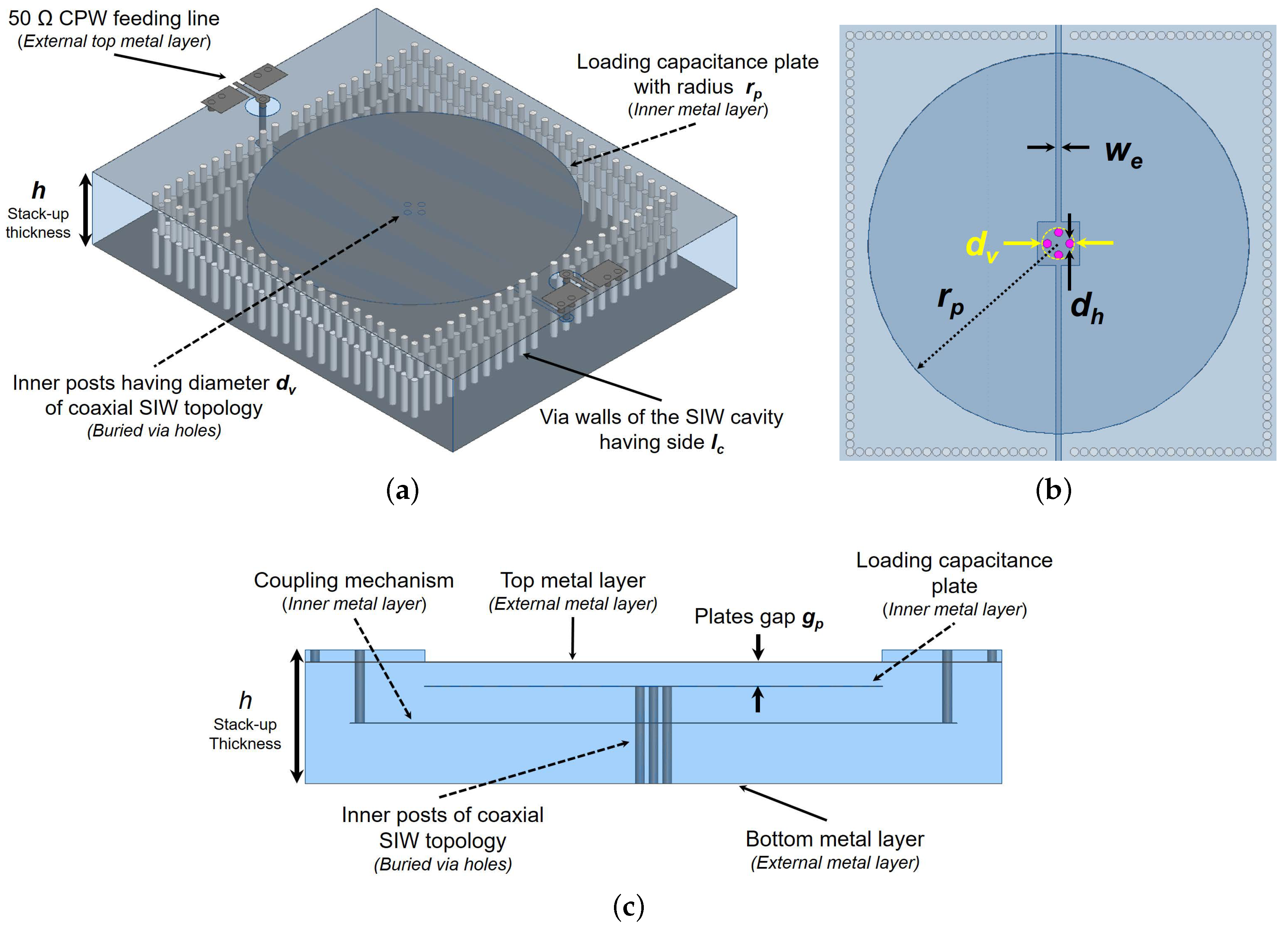
The layout and the main design parameters of an embedded CSIW resonator are shown in Figure 1. Such a structure consists of a square or circular SIW cavity where several plated via holes have been inserted at the center of the cavity resonator, as was first introduced in [4], and then demonstrated in [5,6]. By connecting one end of it via holes to ground, the inductive section of a coaxial resonator is created and controlled by adjusting the position and the diameter of the via holes. Conversely, at the other end of the via holes, a circular metal plate with radius is introduced, as shown in Figure 1b. Such a metal plate is located right below the external top metal layer, which is basically a ground plane, creating a small separating gap filled with dielectric material that we named (visible in Figure 1c).
By doing that, the strong electric field across the gap creates the integrated of a typical combline configuration. This topology enables the implementation of extremely high loading capacitances towards ground, because it is possible to increase the disk plate area considerably while keeping as narrow as possible. The capacitive component of the CSIW can be clearly seen by observing the field line distribution shown in Figure 2. It is worth mentioning that in the selected LTCC fabrication process, depends on the number and thickness of the dielectric tape layers that separate the circular disk plate from the top ground plane.
In addition, the electrical length of the coaxial transmission line embedded into the substrate depends on the final stack-up thickness, thus becoming an important design parameter since it controls both resonant frequency and unloaded Q () of the CSIW resonator [5]. Finally, the inner via holes with diameter have been symmetrically placed around the cavity center to emulate a wider circular inner conductor that would show a fictitious diameter named (see Figure 1b). The further apart the via holes are, the larger the diameter . This enables us to finely set by using only the recommended value for that, in the LTCC manufacturing, should be similar to the dielectric tape thickness to enable a good via filling process.
2.1. Synthesis
As proposed in [9,14] for the CSIW topology with a loading capacitance created by an air isolating gap, the resonator main parameters can be extracted straightforwardly, considering it as a piece of circular-square coaxial line of length (where ) and characteristic admittance embedded into the dielectric substrate. Then, such elements can be modeled as a TEM-mode transmission line short-circuited at one end and terminated with a capacitor on the other. Therefore, the TEM-mode resonant frequency is given by the condition , being the susceptance B of the coaxial resonator defined as
where is the TEM-mode propagation constant, and is the coaxial resonator characteristic impedance. It should be noted that the resonator electrical length at the desired working frequency corresponds to .
Next, the characteristic impedance of the CSIW resonator, and the proportion between the SIW cavity side and value are obtained from [14] as
Thus, the synthesis procedure proceeds by setting the resonator slope parameter b at center frequency of the desired filtering response. As has been explained in [15], the susceptance slope parameter b for resonators with zero susceptance at is well approximated by
On the one hand, the coaxial line admittance can be calculated by using the approximation proposed in [16] for a circular inner conductor of diameter and an external square contour of side , which is
where is the dielectric substrate permittivity of the LTCC dielectric tape.
On the other hand, the loading capacitance between the circular disk and the top metal layer may be written as
where is the permittivity of the free space, is the associated parallel plate capacitance, and is the capacitance due to the fringing effect of the field between the edges of the plates, which are visible in the right part of Figure 2. A correcting factor has been taken into account, due to the specific configuration of the implemented parallel plate capacitor of the CSIW resonator that shows only one circular disk plate. Indeed, the other plate consists of the wider top ground plate. Thus, as demonstrated in [17], the fringing effect of a parallel plate capacitor composed of two identical circular disks can be well approximated as
Finally, to finely tune , a quick optimization of the circular disk plate radius by means of 3D EM simulations is usually required, which includes the metal layer thickness t of the conducting layer that forms the plate.
2.2. Resonator 3D EM Simulations
To perform the study of the performance of a CSIW resonator, let us consider a benchmark configuration with center frequency GHz and using a 10-layer LTCC stack-up, whose layout has been already shown in Figure 1. Regarding the dielectric material, the DuPont™ Green Tape™ 9K7 substrate (, tan @ 10 GHz) has been chosen due to its very low loss tangent. Each dielectric tape layer has a thickness of 0.254 mm in the green state, while the fired thickness is 0.224 mm on account of the shrinkage effect in the z-direction after the LTCC firing step. This means that the total thickness of the 10-layer stack-up of the CSIW resonator is 2.24 mm.
Since we wanted to boost the miniaturization of the device with respect to standard SIW structures, we set a high value for the slope parameter, which is mS. As a result, the main parameters of the CSIW resonator become: pF and . The main dimensions of the compact CSIW resonator considered in this study are shown in Table 1, where is the pitch between adjacent via holes forming the cavity sides. It is worth mentioning that the value of the capacitor plate separation (i.e., mm) has been achieved by introducing the circular disk plate after two dielectric tape layers below the external top metal layer in the stack-up. Thus, the length of the embedded coaxial line is mm mm) mm, which corresponds to an electrical length of @ 1.5 GHz.
These values emphasize the remarkable degree of miniaturization that can be simply achievable with the CSIW topology. Indeed, the SIW cavity side is just mm, which corresponds to and , where is the guided wavelength at GHz.
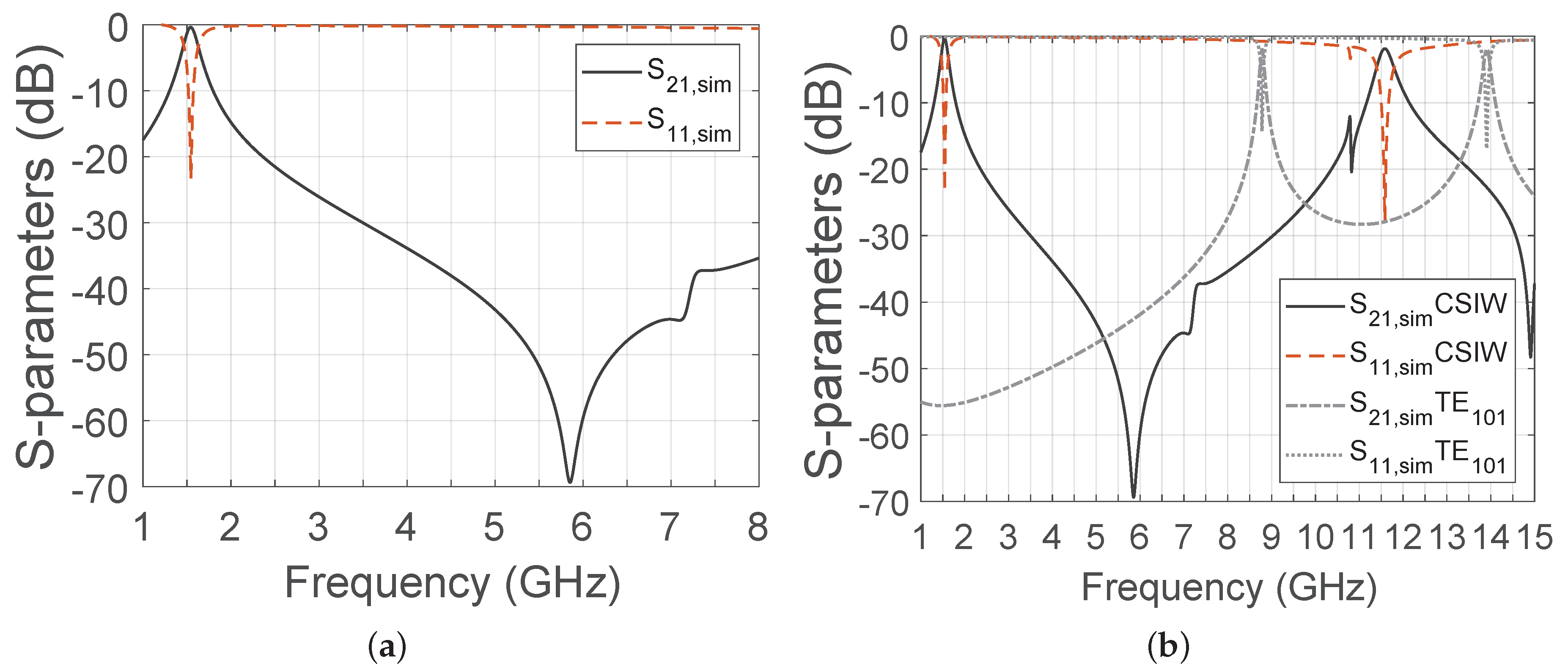
The simulated frequency response of the designed device, which has been obtained by using ANSYS HFSS software, is depicted in Figure 3a, and it is compared to the frequency response of a standard TE-based SIW resonator having the same cavity size in Figure 3b. As shown, the use of an embedded CSIW topology enables also the shifting down of the fundamental mode of the SIW cavity resonator (i.e., the TEM mode in a CSIW resonator) with respect to the first spurious mode, which is the TE mode, thus widening the stop-band bandwidth. Indeed, the EM field of the first spurious mode is altered due to the inner via holes and capacitive patch that provoke an increase of its resonant frequency, from 8.79 GHz as fundamental mode of a TE-based resonator to 11.6 GHz as first spurious mode of the CSIW resonator. Thus, in the proposed simulated CSIW structure, the stop-band bandwidth is greater than , as can be seen in Figure 3b.
Furthermore, Figure 4 shows how the resonant frequency () and of the CSIW resonator change as the function of the radius of the capacitive disk, which means modifying the total value. It is evident that the resonant frequency can be controlled over a wide frequency band (i.e., >1.5 GHz) without affecting the overall resonator dimensions, while keeping a constant over frequency.
In this context, Table 2 provides the comparison between , area miniaturization factor (MF, which has been defined in [18]) and spurious-free band of the designed embedded CSIW resonator and standard TE-based SIW cavity resonators, centered also at GHz and implemented in the very same LTCC stack-up.
Specifically, the MF for a particular miniaturized resonator operating at of is calculated using
where is the area of a standard TE SIW resonator centered at and is the area of the proposed CSIW resonator.
Please note that two thickness layers have been considered for the standard SIW implementation to evaluate the effect on the . As shown in Table 2, CSIW topology enables extremely high miniaturization of the resonator with moderate degradation of and improved stop-band performance.
2.3. Coupling Mechanisms
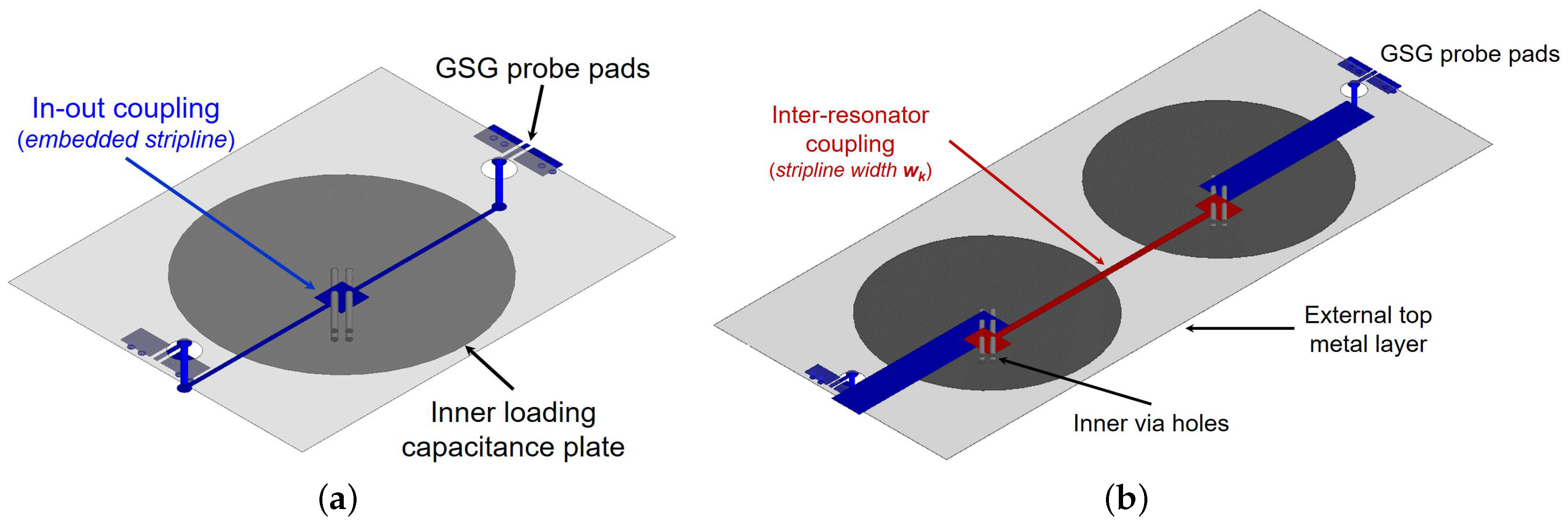
Figure 5 depicts the topology of the novel magnetic coupling mechanism that is especially suited for obtaining strong coupling values in highly loaded CSIW resonators. Specifically, Figure 5a shows the layout of the magnetic external coupling mechanism, while the inter-resonator coupling mechanism is shown in Figure 5b. As reflected, the magnetic couplings are based on embedded stripline probes that are arranged at different layers of the LTCC stack-up, so that inner conductors of adjacent CSIW resonators can be short-circuited between them in a similar manner to conventional tapped-line couplings widely used in combline planar filters. Thus, this solution exploits the high flexibility of the LTCC multi-layer technology to improve the performance of CSIW filters.
By changing the height of the interconnection between coupling probes and the plated via holes forming the inner conductor, the coupling magnitude can be coarsely tuned, as shown in Figure 6. In this context, let us name the height position in the stack-up of the external and the inter-resonator couplings as and , respectively. In addition, let us set mm at the external bottom level and mm at the external top level, for .
In Figure 6a, the external quality factor () is represented as functions of , while the inter-resonator coupling coefficient () between two adjacent resonators versus is shown in Figure 6b. Taking into account that the height position of the circular disk plate corresponds to mm, the highest coupling value is achieved when the stripline probes are short-circuited to this capacitive plate element. By contrast, the coupling drops quickly as the probe is moved towards the bottom layer. Please note that such coupling values enable the design of wideband BPF with FBW easily higher than .
Nevertheless, a fine tuning of both couplings is achieved by varying the stripline probe width, which are named for external coupling and for inter-resonator coupling, as it can be seen in Figure 7a,b, respectively. Thus, once the height position of the coupling probes is defined in the LTCC stack-up, the probe widths allow us to finely control and values, enabling a good optimization of the filtering response.
2.4. 3D EM Simulations of the Filter
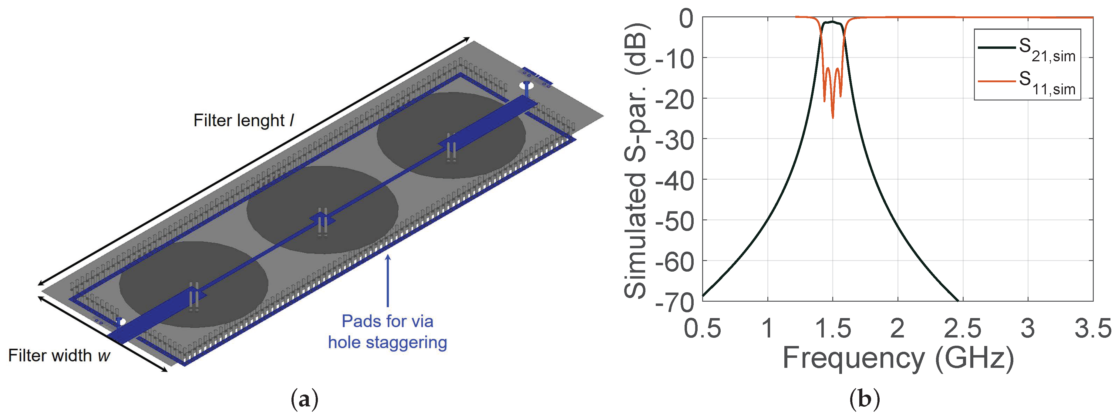
To validate the concept, a CSIW BPF has been designed and simulated. The CSIW resonator previously introduced is the building block of this three-pole BPF whose frequency response will be centered at the L-band. Figure 8a shows the layout of the BPF including its main dimensions. Blue elements highlight the coupling mechanisms, and cover pads that keep an excellent electrical connection among via holes forming the SIW cavity walls on different layers. It should be noted that external and inter-resonator coupling have been accommodated on the very same layer (i.e., mm) thus allowing for a stack-up simplification and manufacturing cost reduction. Indeed, the designed CSIW components have been included in a multi-project LTCC fabrication run that had an already predefined LTCC stack-up. In this context, the inner conductor printing was only allowed at mm, which limits the filter design flexibility. However, optimized values of the coupling coefficients have been easily obtained by adjusting the probe widths and .
We have chosen to design a direct-coupled three-pole Chebyshev filtering response centered at GHz with an equi-ripple bandwidth (BW) of 150 MHz, which corresponds to FBW and return loss (RL) of 15 dB. Thus, the coupling coefficients associated with the target response are , and . Figure 8b depicts the simulated filtering response. In the passband, the minimum insertion loss (IL) is 1.2 dB at 1.49 GHz, while RL are better than 14.5 dB. Finally, the main dimensions of the filter are detailed in Table 3.
3. Results
As previously mentioned, the DuPont™ Green Tape™ 9K7 substrate has been chosen as LTCC dielectric tape in these designs. This is a low-loss glass ceramic dielectric tape for high-frequency applications that includes compatible gold and silver conductors. The final filter stack-up consists of 10 dielectric tape layers with un-fired thickness of 0.254 mm. Then, an additional tape with un-fired thickness of 0.127 mm has been added on the top of the tenth layer to implement the input-output feeding lines and ground-signal-ground (GSG) probe pads for measuring purposes.
Due to the high number of layers in the stack-up, standard LTCC design rules recommend staggering via holes vertically (i.e., zig-zag position of the holes between layers) to limit the via-posting problem. The latter is a protrusion of the via hole at the external layers to the different z-shrinkage of the via fill paste and the tape material, which can provoke metal layer deformations. This technique has been applied in this design as can be seen in Figure 8a.
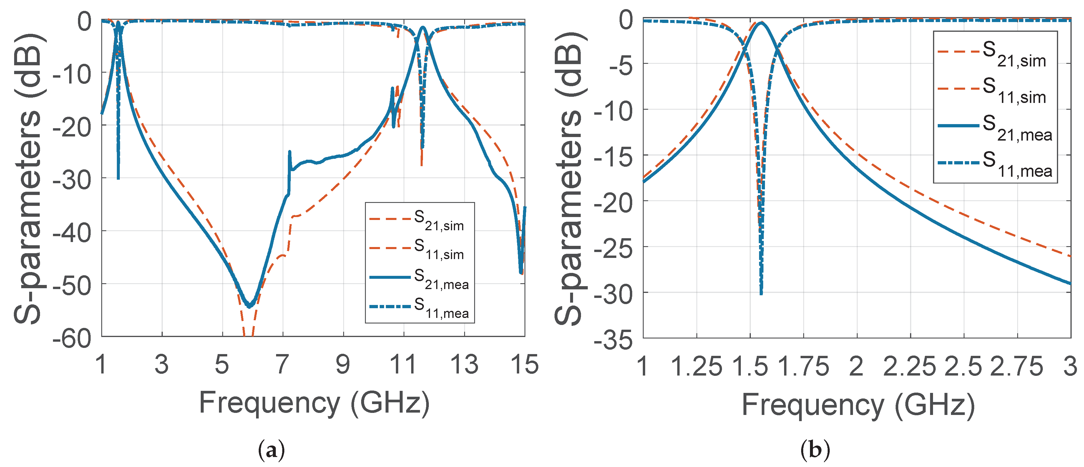
First, the CSIW resonator presented in Section 2.2 has been fabricated and measured. A photograph of a prototype of the CSIW resonator is shown in Figure 9, while the measured results are shown in Figure 10. The agreement between the simulations and measurements is excellent. The TEM resonant frequency is GHz, which is just more than the simulated value, while the spurious-free band is around . In fact, the first high-order mode (i.e., the TE) is centered at 11.6 GHz.
In addition, the extracted from measurements is very similar to the simulated one, both being around 150. This value is slightly lower than those represented in Figure 3. Indeed, the CSIW resonators are fabricated in the very same stack-up of the three-pole BPFs, thus they share the same coupling arrangement that results in a more coupled resonators (i.e., measured dB).
On the other hand, Figure 11b shows a photograph of an embedded CSIW filter prototype, while the comparison between measured and simulated results are depicted in Figure 12. Again, the agreement between simulations in Ansys HFSS and measurements is excellent. Basically, there is no frequency shift between responses, thus validating the proposed topology and its LTCC manufacturing. The filter IL and RL are 1.2 dB and around 15 dB, respectively, while the filter FBW is as expected. The extracted from measurements is close to 165, thus validating the study of Section 2.2.
The filter shows a stop-band bandwidth of more than 8 GHz, up to 10 GHz, with a rejection always better than 30 dB. This means that the spurious-free band is greater than , which is very close to the performance of the designed CSIW resonator. Concerning the discrepancy between simulated and measured stop-band performance, this could be due to the probe station setup. Finally, the filter size is mm, which corresponds to and , where is the guided wavelength at GHz.
Discussion
To sum up, the designed three-pole filter achieves a MF of while providing a quite wide passband with FBW = , very wide spurious-free band with a resonator greater than 160. The latter values confirm the optimal trade-off between remarkable miniaturization design, and wideband filtering response of the proposed magnetic coupling mechanism for embedded CSIW components. In this context, the filter performance in terms of FBW, MF, and spurious-free band of this work are summarized and compared to related references in Table 4.
Wideband filtering responses are extremely complicated to implement in miniaturized SIW BPFs, especially if the MF is strongly increased. For instance, such characteristics have been latterly achieved in [8] by using a combination of eight-mode SIW resonators with CRME structures. However, such an approach enables the MF to be higher than at the cost of a low , which has been extracted to be just 90.
As a comparison, in [5], the authors proposed a three-pole embedded CSIW filter centered at 2.14 GHz with FBW whose resonators have an area of mm, which means that the MF is around . In [18], the designed two-pole and three-pole BPFs based on HMSIW and QMSIW resonators showed passband FBWs of and , respectively, at UHF band. However, in the case of the trisection filters, the achieved MF was below .
Finally, some recent works proposed the use of conventional multi-layer PCB technology to implement miniaturized SIW filters based on coaxial topologies. As has been presented in [13], the FBW of the two four-pole CSIW BPFs centered at UHF band is if MF = 92.4%, but is reduced to when the MF is increased up to because standard magnetic post-wall irises were used to couple adjacent CSIW resonators. On the contrary, in [19], third-order BPFs were designed and tested by arranging side-by-side three vertical coaxial stepped-impedance resonators (SIRs), showing an extremely high MF, good , but limited spurious-free band.
4. Conclusions
In this paper, the design of miniaturized embedded CSIW resonator filters with wideband responses has been investigated. A novel magnetic coupling mechanism has been proposed and studied in detail for both external and inter-resonator couplings. By combining short-ended stripline probes and multi-layer LTCC manufacturing, we can implement extremely compact BPFs with a reasonable level of losses, as well as increase the maximum achievable passband bandwidth in embedded CSIW technology. All concepts have been validated by the simulation and measurement of some fabricated proof-of-concept filtering devices.
Author Contributions
Conceptualization, S.S., J.D.M. and V.E.B.; Funding acquisition, J.D.M. and V.E.B.; Investigation, S.S. and J.D.M.; Methodology, S.S. and J.D.M.; Project administration, J.D.M. and V.E.B.; Resources, S.S.; Supervision, J.D.M. and V.E.B.; Validation, S.S.; Visualization, S.S.; Writing-original draft, S.S.; Writing-review & editing, J.D.M. and V.E.B.
Funding
This research was funded by Ministerio de Economía, Industria y Competitividad, Spanish Government, under Research Project TEC2016-75934-C4-3-R.
Conflicts of Interest
The authors declare no conflict of interest. The founding sponsors had no role in the design of the study; in the collection, analyses, or interpretation of data; in the writing of the manuscript, and in the decision to publish the results.
Abbreviations
The following abbreviations are used in this manuscript:
| EM | Electromagnetic |
| BPF | Bandpass Filter |
| PCB | Printed Circuit Board |
| LTCC | Low-Temperature Co-fired Ceramics |
| SIW | Substrate Integrated Waveguide |
| CSIW | Coaxial Substrate Integrated Waveguide |
| QMSIW | Quarter-Mode SIW |
| HMSIW | Half-Mode SIW |
| CRME | Circular-Ring Miniaturize Element |
| UMTS | Universal Mobile Telecommunications Service |
| LTE | Long-Term Evolution |
| UHF | Ultra High Frequency |
| BW | Bandwidth |
| FBW | Fractional Bandwidth |
| TEM | Transverse Electromagnetic |
| SIR | Stepped-Impedance Resonator |
| MF | Miniaturization Factor |
| GSG | Ground-Signal-Ground |
| HFSS | High-Frequency Structure Simulator |
| IL | Insertion Loss |
| RL | Return Loss |
| Q | Quality factor |
| Unloaded Quality factor | |
| External Quality factor | |
| Inter-resonator Coupling Coefficient |
References
- Chen, X.P.; Wu, K. Substrate integrated waveguide filters: Practical aspects and design considerations. IEEE Microw. Mag. 2014, 15, 75–83. [Google Scholar] [CrossRef]
- Matthaei, G.L. Combline band-pass filters of narrow or moderate bandwidth. Microw. J. 1963, 6, 82–96. [Google Scholar]
- Rhodes, J.D. The stepped digital elliptic filter. IEEE Trans. Microw. Theory Technol. 1969, 17, 178–184. [Google Scholar] [CrossRef]
- Hoeft, M.; Ishizaki, T.; Nakakubo, H. Laminated rf Device with Vertical Resonators. Jpn. Patent No. EP 2 068 393 A1, June 2009. [Google Scholar]
- Turgaliev, V.; Kholodnyak, D.; Vendik, I.; Stöpel, D.; Humbla, S.; Müller, J.; Hein, M.A. LTCC highly loaded cavities for the design of single- and dual-band low-loss miniature filters. In Proceedings of the 2010 European Microwave Conference (EUMW), Paris, France, 28–30 September 2010; pp. 180–183. [Google Scholar]
- Martínez, J.D.; Taroncher, M.; Boria, V.E. Capacitively loaded resonator for compact substrate integrated waveguide filters. In Proceedings of the 2010 European Microwave Conference (EUMW), Paris, France, 28–30 September 2010; pp. 192–195. [Google Scholar]
- Grigoropoulos, N.; Sanz-Izquiredo, B.; Young, P.R. Substrate integrated folded waveguides (SIFW) and filters. IEEE Microw. Wirel. Compon. Lett. 2005, 15, 829–831. [Google Scholar] [CrossRef]
- Li, L.; Wu, Z.; Yang, K.; Lai, X.; Lei, Z. A novel miniature single-layer eighth-mode SIW filter with improved out-of-band rejection. IEEE Microw. Wirel. Compon. Lett. 2018, 28, 407–409. [Google Scholar] [CrossRef]
- Martínez, J.D.; Sirci, S.; Taroncher, M.; Boria, V.E. Compact CPW-fed combline filter in substrate integrated waveguide technology. IEEE Microw. Wirel. Compon. Lett. 2012, 22, 7–9. [Google Scholar] [CrossRef]
- Kholodnyak, D.; Turgaliev, V.; Vorobev, E. Advanced microwave filters in LTCC and PCB technologies. In Proceedings of the 2014 Asia-Pacific Microwave Conference (APMC), Sendai, Japan, 4–7 November 2014; pp. 88–90. [Google Scholar]
- Turgaliev, V.; Kholodnyak, D.; Müller, J.; Hein, M.A. Small-size low-loss bandpass filters on substrate-integrated waveguide capacitively loaded cavities embedded in low temperature co-fired ceramics. J. Ceram. Sci. Technol. 2015, 6, 305–314. [Google Scholar]
- Nassar, S.O.; Meyer, P. Pedestal substrate integrated waveguide resonators and filters. IET Microw. Antennas Propag. 2017, 11, 804–810. [Google Scholar] [CrossRef]
- Ho, M.H.; Li, J.C.; Chen, Y.C. Miniaturized SIW cavity resonator and its application in filter design. IEEE Microw. Wirel. Compon. Lett. 2018, 28, 651–653. [Google Scholar] [CrossRef]
- Sirci, S.; Sánchez-Soriano, M.Á.; Martínez, J.D.; Boria, V.E.; Gentili, F.; Bösch, W.; Sorrentino, R. Design and multiphysics analysis of direct and cross-coupled SIW combline filters using electric and magnetic couplings. IEEE Trans. Microw. Theory Technol. 2015, 63, 4341–4354. [Google Scholar] [CrossRef]
- Hong, J.S. Microstrip Filter for RF/Microwave Applications, 2nd ed.; John Wiley and Sons, Inc.: Hoboken, NJ, USA, 2011. [Google Scholar]
- Riblet, H.J. An accurate approximation of the impedance of a circular cylinder concentric with an external square tube. IEEE Trans. Microw. Theory Technol. 1983, 31, 841–844. [Google Scholar] [CrossRef]
- Landau, L.D.; Lifschitz, E.M. Electrodynamics of Continuous Media (Volume 8). In A Course of Theoretical Physics; Permagon Press: Oxford, UK, 1987. [Google Scholar]
- Pourghorban Saghati, A.; Pourghorban Saghati, A.; Entesari, K. Ultra-miniature SIW cavity resonators and filters. IEEE Trans. Microw. Theory Technol. 2015, 63, 4329–4340. [Google Scholar] [CrossRef]
- Yang, T.; Ho, K.; Rebeiz, G.M. Compact self-shielded 2–3 GHz high-Q coaxial fixed and tunable filters. IEEE Trans. Microw. Theory Technol. 2014, 62, 3370–3379. [Google Scholar] [CrossRef]
Figure 1.
3D sketches of an embedded CSIW resonator including main dimensions: (a) top view; (b) detail of the inner conductor and capacitive plate; and (c) lateral view.
Figure 1.
3D sketches of an embedded CSIW resonator including main dimensions: (a) top view; (b) detail of the inner conductor and capacitive plate; and (c) lateral view.

Figure 2.
3D E-field distribution for the proposed embedded coaxial SIW resonator in the gap that separates the disk plate and the top ground plane.
Figure 2.
3D E-field distribution for the proposed embedded coaxial SIW resonator in the gap that separates the disk plate and the top ground plane.

Figure 3.
Simulated wideband response of (a) the proposed CSIW resonator having mS; (b) Comparison between the frequency response of the proposed CSIW resonator (solid lines) and a standard TE-based SIW resonator (dashed lines) having the same cavity size.
Figure 3.
Simulated wideband response of (a) the proposed CSIW resonator having mS; (b) Comparison between the frequency response of the proposed CSIW resonator (solid lines) and a standard TE-based SIW resonator (dashed lines) having the same cavity size.

Figure 4.
(a) Resonant frequency versus circular disk plate radius ; (b) Resonator versus for the same variation of of (a).
Figure 4.
(a) Resonant frequency versus circular disk plate radius ; (b) Resonator versus for the same variation of of (a).

Figure 5.
Layout of the proposed magnetic (a) external and (b) inter-resonator coupling mechanisms based on stripline probes short-circuited to the inner posts of the CSIW resonators. Please note that bottom layer and via holes that form the SIW cavity walls are not shown for improving readability.
Figure 5.
Layout of the proposed magnetic (a) external and (b) inter-resonator coupling mechanisms based on stripline probes short-circuited to the inner posts of the CSIW resonators. Please note that bottom layer and via holes that form the SIW cavity walls are not shown for improving readability.

Figure 6.
(a) and (b) variation versus height of stripline probe in the stack-up expressed as layer number (, ).
Figure 6.
(a) and (b) variation versus height of stripline probe in the stack-up expressed as layer number (, ).

Figure 7.
(a) variation versus stripline probe width when . (b) variation versus stripline probe width when .
Figure 7.
(a) variation versus stripline probe width when . (b) variation versus stripline probe width when .

Figure 8.
(a) Three-pole BPF filter layout; (b) Simulated frequency response.

Figure 9.
Photo of the CSIW resonator prototype.

Figure 10.
Measured and simulated results of the embedded coaxial SIW resonator: (a) wideband response up to 15 GHz and (b) passband of the resonance.
Figure 10.
Measured and simulated results of the embedded coaxial SIW resonator: (a) wideband response up to 15 GHz and (b) passband of the resonance.

Figure 11.
(a) Photograph of some layers of the LTCC stack-up (i.e., from top to bottom, via holes punching and after printing the coupling and capacitive patch, respectively). The resonator layout is also visible at the sides of the photograph; (b) Photograph of three-pole BPF prototype.
Figure 11.
(a) Photograph of some layers of the LTCC stack-up (i.e., from top to bottom, via holes punching and after printing the coupling and capacitive patch, respectively). The resonator layout is also visible at the sides of the photograph; (b) Photograph of three-pole BPF prototype.

Figure 12.
Measured and simulated results of the three-pole BPF: (a) wideband response and (b) filter passband.
Figure 12.
Measured and simulated results of the three-pole BPF: (a) wideband response and (b) filter passband.


Table 1.
Layout Dimensions of the Designed CSIW Resonator (Unit: mm).
| h | ||||||||
|---|---|---|---|---|---|---|---|---|
Table 2.
Comparison of coaxial SIW topology versus standard TE-based SIW topology.
| SIW Topology | Area (mm) | MF (%) | (%) | Spurious-Free Band | |
|---|---|---|---|---|---|
| TE (h = 2.25 mm) | 2704 | 253 | |||
| TE (h = 1.12 mm) | 2704 | 0 | 213 | ||
| Coaxial | 209 |
Table 3.
Layout Dimensions of the Three-Pole CSIW Filter (Unit: mm).
| l | w | h | |||||||||||
|---|---|---|---|---|---|---|---|---|---|---|---|---|---|
| 32 |
© 2019 by the authors. Licensee MDPI, Basel, Switzerland. This article is an open access article distributed under the terms and conditions of the Creative Commons Attribution (CC BY) license (http://creativecommons.org/licenses/by/4.0/).
Share and Cite
MDPI and ACS Style
Sirci, S.; Martínez, J.D.; Boria, V.E. A Novel Magnetic Coupling for Miniaturized Bandpass Filters in Embedded Coaxial SIW. Appl. Sci. 2019, 9, 394. https://doi.org/10.3390/app9030394
AMA Style
Sirci S, Martínez JD, Boria VE. A Novel Magnetic Coupling for Miniaturized Bandpass Filters in Embedded Coaxial SIW. Applied Sciences. 2019; 9(3):394. https://doi.org/10.3390/app9030394
Chicago/Turabian StyleSirci, Stefano, Jorge D. Martínez, and Vicente E. Boria. 2019. "A Novel Magnetic Coupling for Miniaturized Bandpass Filters in Embedded Coaxial SIW" Applied Sciences 9, no. 3: 394. https://doi.org/10.3390/app9030394
Note that from the first issue of 2016, this journal uses article numbers instead of page numbers. See further details here.