Charge-Line Dual-FET High-Repetition-Rate Pulsed Laser Driver

Warsaw University of Technology, Institute of Electronic Systems, 00-665 Warsaw, Poland
*
Author to whom correspondence should be addressed.
Appl. Sci. 2019, 9(7), 1289; https://doi.org/10.3390/app9071289
Submission received: 1 March 2019
/
Revised: 22 March 2019
/
Accepted: 24 March 2019
/
Published: 27 March 2019
(This article belongs to the Special Issue Ultrafast Laser Pulses)
Abstract
:Most modern pulsed laser systems require versatile laser diode drivers. A state-of-the-art pulsed laser driver should provide precise peak power regulation, high repetition rate, and pulse duration control. A new, charge line dual-FET transistor circuit structure was developed to provide all these features. The pulsed modulation current is adjustable up to Imax = 1.2 A, with the laser diode forward voltage acceptable up to UF max = 20 V. The maximum repetition rate is limited by a charge line circuit to frep max = 20 MHz. Compared to the conventional single transistor drivers, the solution proposed in this paper allows a precise, high resolution width regulation to be obtained, whereas a low pulse jitter is ensured. In the solution, two separate, out-of-phase signals are used to trigger the individual Field Effect Transistors (FET). The resultant pulsed modulation current full-width-at-half-maxima (FWHM) is regulated from ~200 ps up to 2 ns. All control and timing signals are generated with a popular Field-Programmable Gate Array (FPGA) digital circuitry. The use of standard FPGA devices ensures the low cost and high reliability of the circuit, which are not available in laser drivers consisting of sophisticated analogue adjustable delay circuits.
1. Introduction
Nowadays, high-power short laser pulses are the subject of great interest in many fields of application, e.g., Light Detection and Ranging (LIDAR) [1,2], time resolved spectroscopy [3], or picosecond gain switched lasers [4]. The pulsed current source might also be applied to the electrically tunable Near Infra-Red (NIR) [4] or Quantum Cascade Lasers [5]. However, the main application of the solution presented in this paper is the seed laser driver for high-power (kW-level) fiber lasers. Optical pulse quality and reproducibility are vital for a stable and reliable operation of the whole fiber laser system.
The direct modulation of the semiconductor laser current is a commonly used technique to produce fast optical pulses [1,2,6,7,8] and has the advantage of simple and inexpensive operation. Many different topologies have been discussed so far [1,2,6,7]; however, noise parameters are rarely recalled. Considering those facts, a novel direct laser current modulator was designed and constructed resulting in the outstanding noise and switching properties.
2. Foundation of Charge-Line Pulsed Laser Driver
2.1. Dual-FET Output Stage Topology
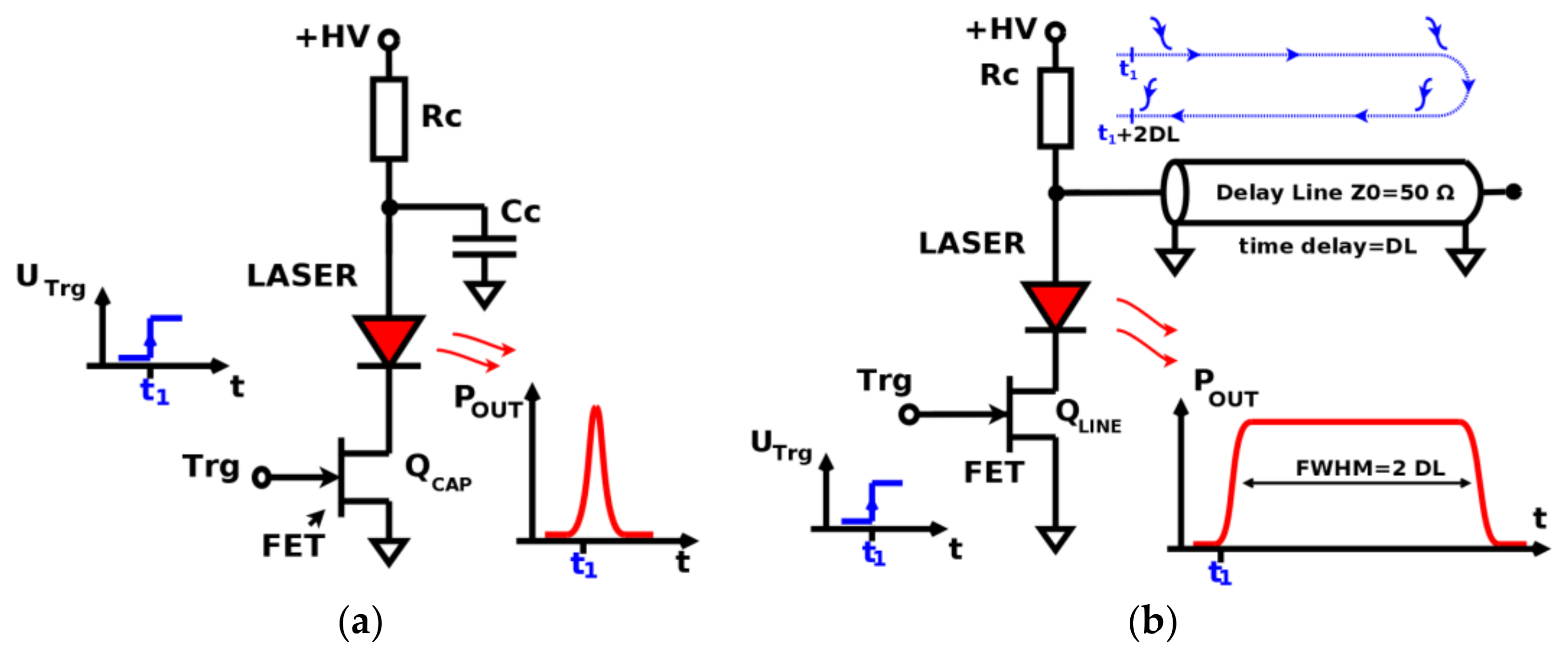
One of the most popular solutions dedicated to high-power drivers utilizes single switching devices [1,2,6,7]. For this reason, the avalanche transistors for over 60 years [9] were the commonly used devices in laser pulsed generators [6,7]. However, nowadays most of the modern systems utilize Field Effect Transistors (FET) [1,2]. The basic example topologies, shown in Figure 1, are based on charge storage passive elements. In order to briefly analyze their principle of operation, a steady state (transistors are switched-off and storage elements are charged) is assumed.
If the trigger signal is applied, the CC capacitor in Figure 1a is discharged through a semiconductor switch and a laser diode, resulting in an optical pulse of Gaussian shape [1,2]. The amplitude of the laser pulse is determined both by the +HV voltage applied to the driver, and the CC capacitance. Therefore, it is impossible to adjust the pulse width and amplitude separately. Nevertheless, the main advantage of this simple circuit is its high laser current [1,6], limited only by the parasitic inductances and resistances of the Cc, QCAP, and laser diode itself.
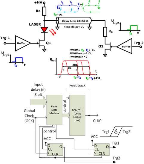
In the other topology, which is shown in Figure 1b, an open-end delay line was utilized as a charge storage element. When the trigger signal (denoted as Trg) is applied, the transistor QLINE starts to discharge the line. The delay line acts then as a constant current sink (the peak current is determined by the characteristic impedance Z0 of the transmission line and initial line voltage) by the time needed by the falling edge signal to propagate back and forth through the passive element. The duration of the optical pulse resulting from the square wave applied to the laser is approximately 2 ∙ DL, thus a pulse width adjustment is possible only by replacing the physical element (i.e., the delay line). On the other hand, the peak power is independent of the pulse timing and might be adjusted by the +HV voltage setting.
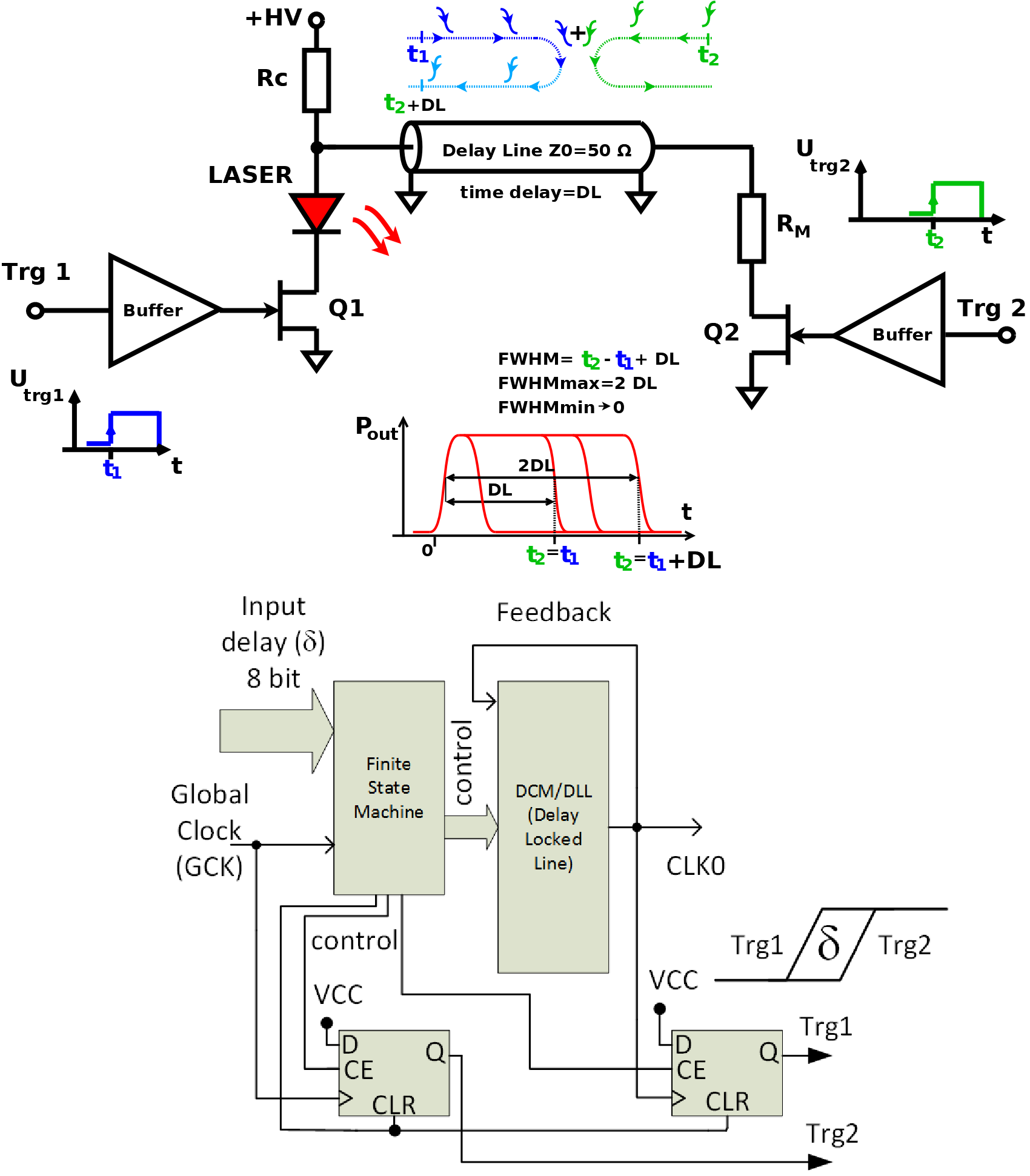
The novel topology of the pulsed laser driver described in this paper is shown in Figure 2. It combines two symmetrical structures from Figure 2b, although a single shared delay line is used [7]. The operation of the circuit can be divided into two adjacent phases. During the first phase, the transistor Q1 is switched on at time t1 and a pre-charged delay line supplies the laser diode (assures the current flow). If no trigger signal is applied to the Q2, the resulting optical pulse width is 2 ∙ DL, as in the circuit shown in Figure 1b. However, if a second trigger signal is also supplied to the Q2 in the succeeding second phase, i.e., t2 = t1, the transistors Q1 and Q2 start to discharge the delay line at the same time. This causes the premature termination of the lasing current at time t1 + DL. By adjusting the mutual position t2 and t1 in the time domain, according to Equation (1), the available regulated laser pulse width ranges from 0 to 2 ∙ DL.
where tFWHM MIN → 0 and tFWHM MAX = 2 ∙ DL
tFWHM = t2 − t1 + DL
The lasing peak current is adjusted via the +HV voltage, applied to the driver. According to Equation (2), the main current limiting factors in the dual-FET topology are laser forward voltage, Q1-on resistance and Z0 of the delay line.
2.2. Circuit Timing
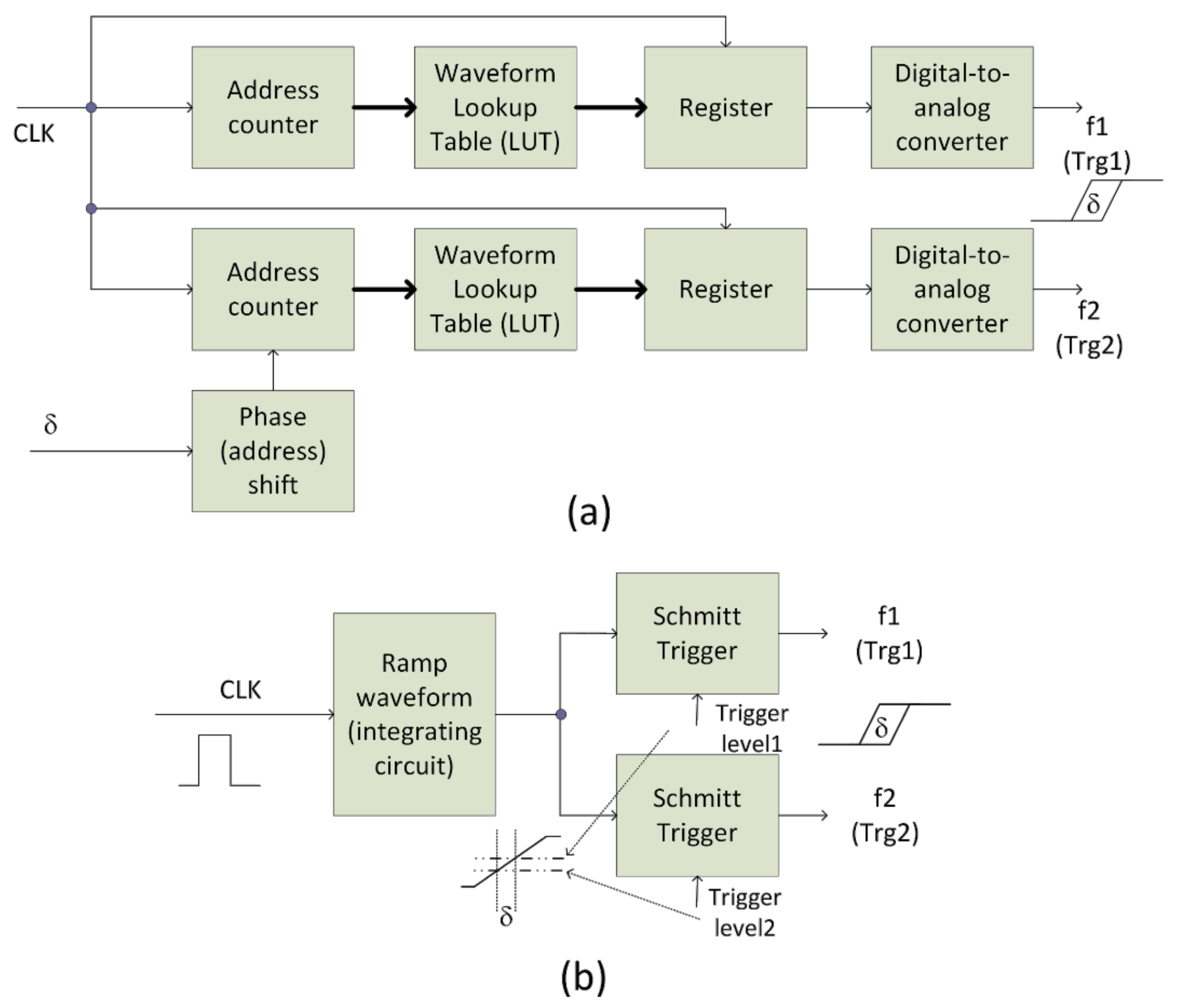
The circuit in Figure 2 requires synchronized clock sources responsible for the triggering of Q1 and Q2. There are common approaches that incorporate either an adjustable delay obtained with the use of either the Direct Digital Synthesis (DDS) circuit (Figure 3a) [10,11,12] or an analogue approach based on the ramp source and a programmable comparator (see Figure 3b) [10,11,12]. The analogue solution is relatively inexpensive; however, several drawbacks of an analogue delay line may decrease the functionality of the laser driver. The first drawback results from the temperature influence on the parameters of component parameters (i.e., capacitance, intrinsic propagation delays, and threshold voltages). Therefore, a thermal compensation of the circuit is necessary. The second drawback results from the noise processes affecting the relative position of the delayed clock slopes. On the contrary, the digital solutions based on the DDS ensuring sub-nanosecond resolutions are expensive or require high clock speeds.
Modern Field-Programmable Gate Array (FPGA) devices offer advanced clocking resources like a Phase Locked Loop (PLL) or a Digital Clock Manager (DCM) [13]. They allow the obtaining of various frequencies, clock delays, and phase shifts within the FPGA device, with the use of just a single external clock source. In the proposed solution we have utilized a modern Xilinx Spartan 6 FPGA device (XC6SLX16), in which the DCM is implemented as a programmable delay line depicted in Figure 4.
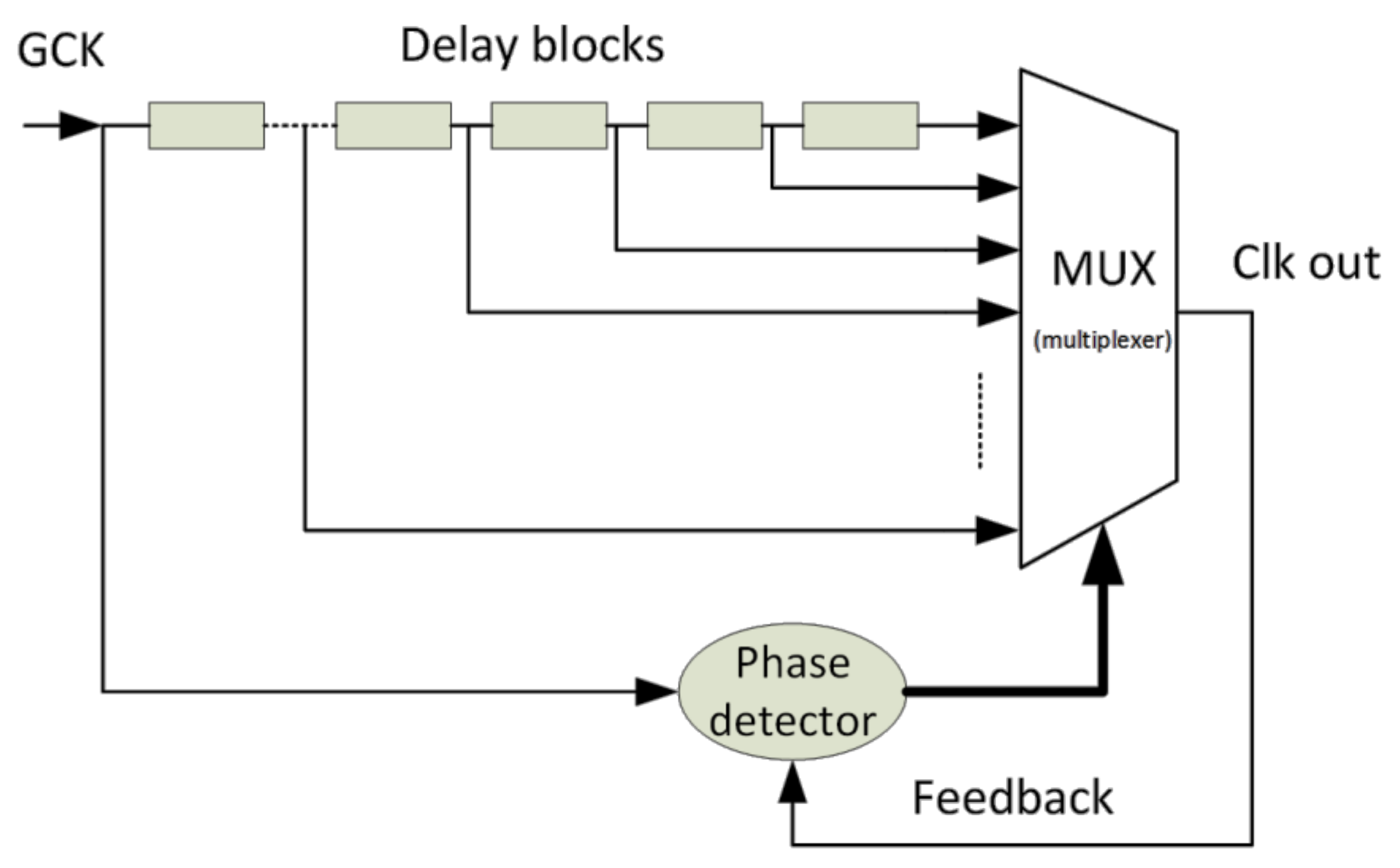
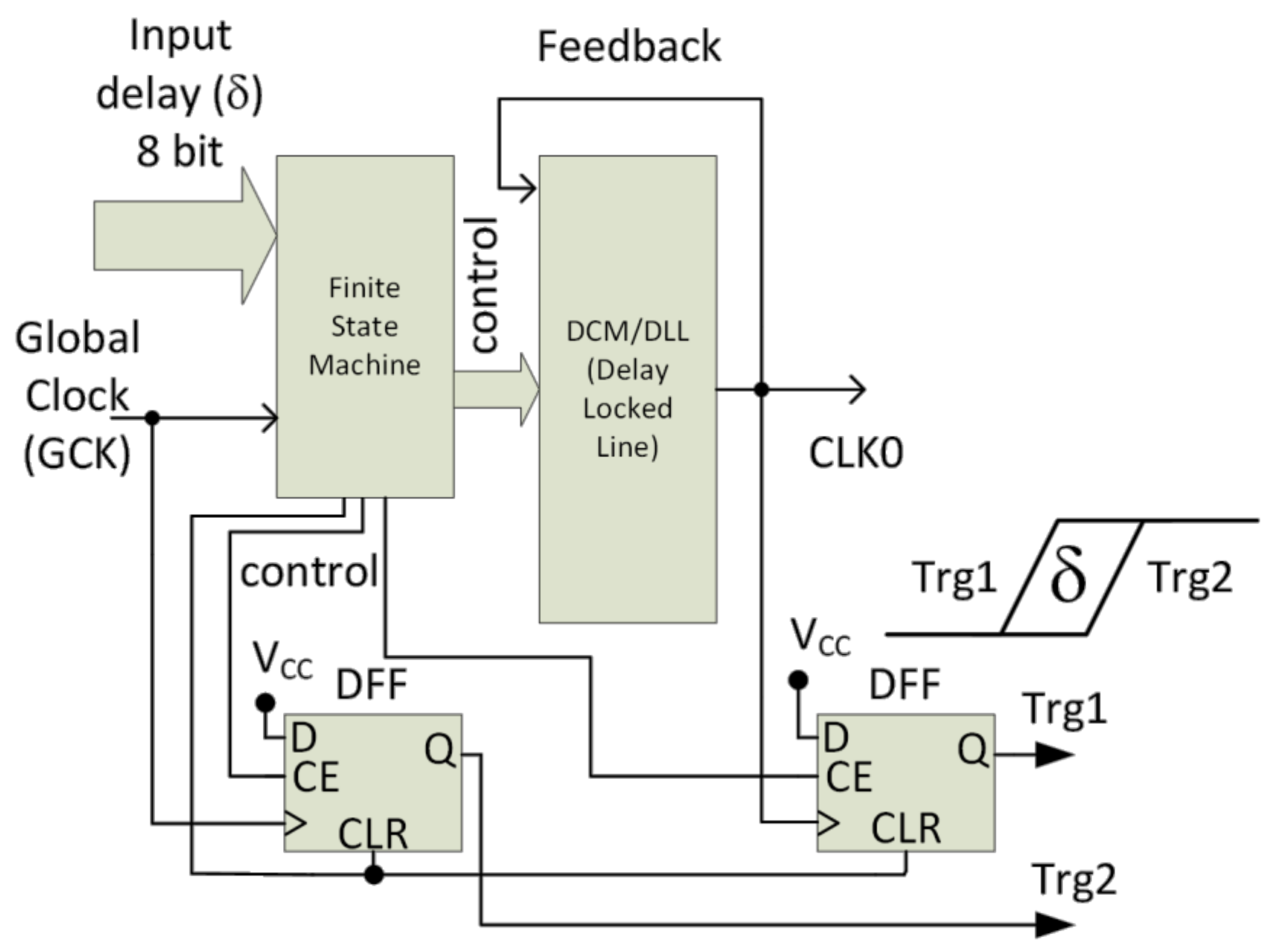
The principle of operation of the device in Figure 4 is based on the phase loop, in which the phase detector alters the delay of the delay chain formed of delay blocks by the adjustment of the multiplexer (MUX). Therefore, the DCM offers both a relatively small jitter and a high resolution (low step). The single-cycle jitter measured with the Agilent 53,200 counter/timer for the XC6SLX16 device used in the proposed laser driver did not exceed 20 ps, whereas the resolution (interval between subsequent steps) was δr = 18 ps. These parameters decide on the overall performance of the circuit proposed in Figure 2; however, further system measurements (see Section 4) show that they are sufficient for our driver’s implementation. In order to ensure total independence from the external circuitry of our solution, we used a 100 MHz crystal clock connected to the global clock source (GCK) of the FPGA. The 100 MHz source was used as the input for the DCM device, which produces an adjustable delay within the 0–2 ns range at the CLK0 output (see Figure 5). This output acted as a timing of a simple digital subcircuit formed of two D flip-flops (DFFs) that was responsible for the repetition frequency limitation of our driver. The GCK and delayed CLK0 clock signals from the DCM were used as the timing sources at the clock inputs of the DFFs. The phase-shifted rising slope (edge) at the clock inputs together with constant positive supply at the data input (D) of the DFF enforce a delayed appearance of logical ‘1’ at the DFF Q outputs. This way we are able to obtain a phase delay (δ) of the rising edges at DFFs outputs (denoted as Q in Figure 5). On the other hand, the Chip Enable (CE) inputs of DFFs allowed us to periodically disable the signal at Q outputs of DFFs. The low logical level at CE inputs disables the laser pulse for a single GCK and CLK0 period, and, as a result, decreases the laser average pulse repetition rate. Therefore, the driver is able to decrease (control) the number of pulses available at Trg1 and Trg2 outputs, which activate the switching transistors (and the laser). After each excitation of the laser, caused by the appearance of logical ‘1’ at Q outputs, a clear (CLR) signal must be applied in order to reset both DFFs and switch off the transistors.
The block diagram of the digital timing circuit is shown in Figure 5, and also contains a Finite State Machine, which is responsible for proper DCM and D flip-flop timing. The Finite State Machine adjusts the delay setting of the DCM according to the 8-bit input value, and ensures the limited repetition rate (output frequency of Trg1 and Trg2, despite the GCK frequency. The output signals Trg1 and Trg2 are directly connected to the input buffers (74AC series) shown in Figure 2.
3. System Implementation
To achieve the best performance of the pulsed laser driver, care must be taken in order to choose adequate transistors and passive elements. Sub-nanosecond high-current switching requires low inductance transmission lines on PCB and dense element placement.
3.1. Tranistor Switches
The proper choice of semiconductor switches was aimed at minimizing the noise and maximizing the driver’s speed of operation. The avalanche transistors exhibit fast and high-current pulses [6,7], but they suffer from the thermal drift and high power loses. On the other hand, large gate and parasitic capacitances of high-power Metal-Oxide Semiconductor (MOS) devices make them suitable only in resonant circuits [1,2]. Therefore, instead of using bipolar or MOS devices, GaN High-Electron-Mobility Transistors (HEMT) with parameters listed in Table 1 were used. HEMTs are modern microwave components used in the pulsed and continuous wave high power Radio-Frequency (RF) devices. They exhibit a very low gate charge and, due to the pulse mode of gate driving applied, fast and high-current switching is achievable.
3.2. Delay Line and Charging Resistor
In the presented solution, approximately 25 cm of a high quality RF coaxial cable was used to obtain the maximum pulse width of approximately tFWHM MAX = 2 ∙ DL = 2 ns. The characteristic impedance of the transmission line is of the commonly used standard, i.e., Z0 = 50 Ω. If the boundary values of parameters in Equation (2) are considered, the maximum lasing current is described by Equation (3).
Each generated pulse discharges the delay line, whereas the recharging process takes place during successive repetitions. The RC resistor supplies the delay line with a time constant τline = RC ∙ Cline, where Cline is approximately 23 pF. In order to ensure a stable pulse amplitude in a wide range of repetition rate (DC to 20 MHz), RC should fully charge the line in the shortest period between the two following pulses at Trg1 and Trg2 (i.e., tmin = 46 ns). If the time constant relation of Equation (4) is assumed, the line will charge to >98% of the final voltage.
τline = 4 ∙ RC ∙ Cline < tmin
RC < 500 Ω
RC < 500 Ω
3.3. Matching Resistor of the Line
If the delay line quenching pulse generated by the Q2 switch has a higher amplitude compared to the pulse generated by Q1, a negative current flow will occur in the laser diode. It may lead to the permanent damage of the laser structure, thus a matching resistor RM was used in the circuit. The RM value was set experimentally to 10 Ω.
3.4. Input Buffers
In the pulse mode, high current transient states in HEMT transistors are observed. Therefore, the process of switching at inputs (gates) of HEMTs should be as short as possible. Moreover, the low inclination of Trg1 and Trg2 rising edges could be easily affected by interferences caused by glitches coming from the switching process of HEMTs. Therefore, in order to ensure the fast switching of the transistors, each input buffer (between FPGA outputs and HEMT gates) combines four connected in-parallel AC family Complementary Metal Oxide Semiconductor (CMOS) logic gates. The buffers’ inputs are directly driven by the FPGA timing subsystem shown in Figure 5.
3.5. +HV DC–DC Converter
The peak pulse power of the laser diode is regulated directly via the +HV supply voltage (see Figure 2). In order to increase the versatility of the laser driver system, a DC–DC converter, regulated from 10 V up to 80 V was implemented.
3.6. PCB Layout
A complete ready-to-use laser driver device is shown in Figure 6a. A two layer PCB and short component connections ensure low impedance current paths. For the test purposes, instead of the laser, a loading resistor RL was connected to the driver’s output.
The trigger signals (Trg1 and Trg2) are routed to the buffers in the top-right side of the dual-FET PCB and are connected to the miniature FPGA board shown in Figure 6b. In order to avoid trigger signal reflections and minimize the jitter of the trigger signals, the FPGA board consists of the line matching resistors at the IO pins.
4. Test Results
4.1. Preliminary Tests of the System
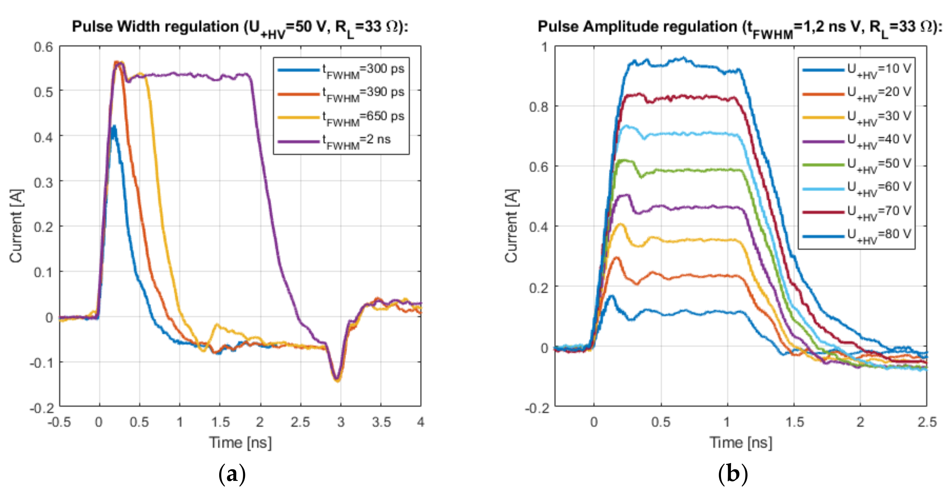
During preliminary tests of the electrical parameters of the presented driver, a resistive load RL = 33 Ω was used. The Figure 7a shows different settings of the FPGA timing signal leading to different intervals obtained at the dual-FET driver. The maximum pulse width is approximately 2 ns, which is in a good agreement with the design assumptions. The measured current-pulse rise times tr 10%–90% < 140 ps and fall times tf 10%–90% < 430 ps are sufficient to generate sub-nanosecond laser pulses. The falling edge negative current undershoot and spike is noticeable in Figure 7a. To compensate this effect, the increase of the matching resistor RM value might be considered.
Figure 7b shows the pulse peak current regulation via +HV voltage adjustment. In the test load configuration (RL = 33 Ω), the maximum peak current of 0.96 A was obtained.
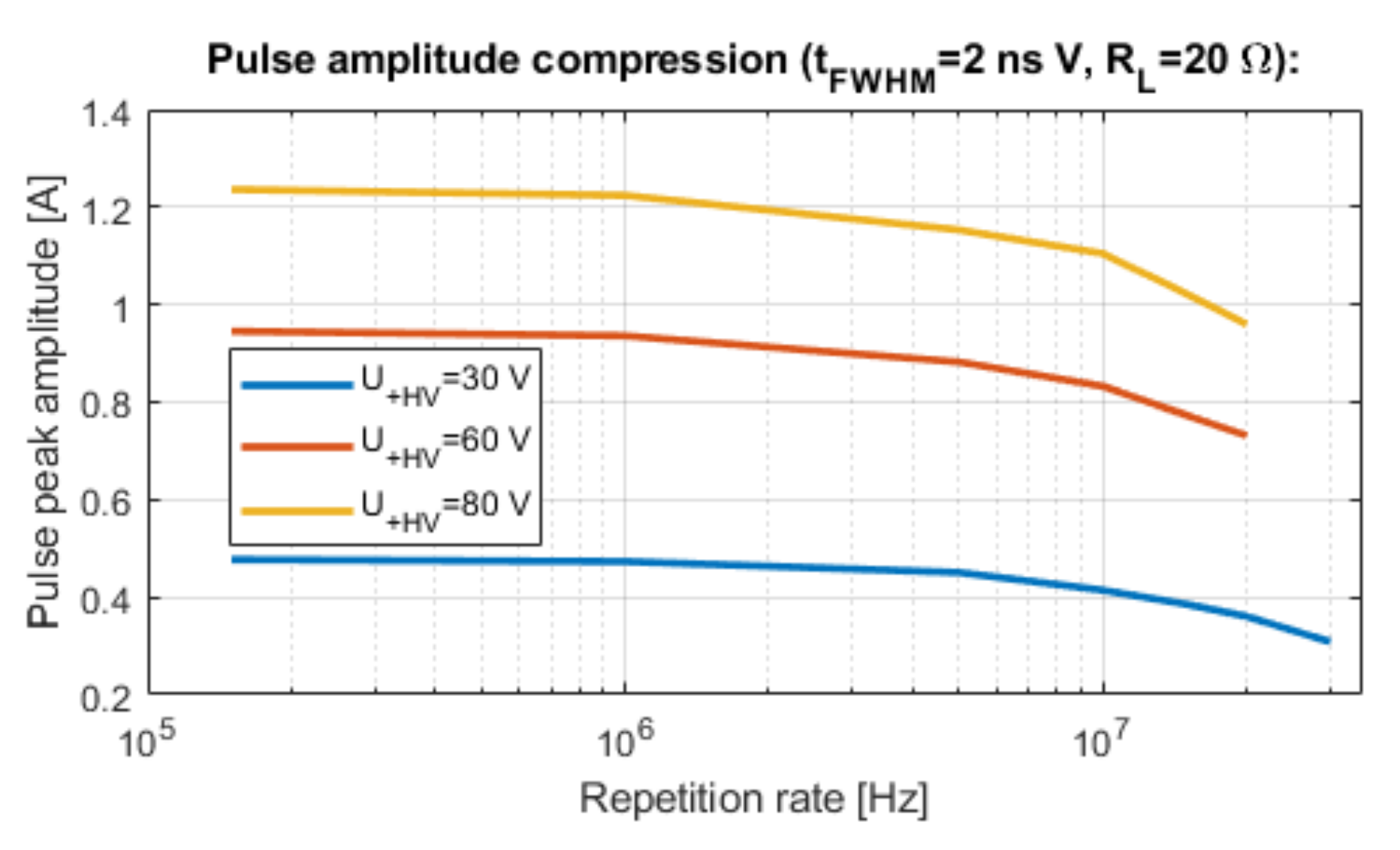
Operating with higher repetition rates leads to the peak power amplitude compression. In Figure 8, a less than 2.5 dB drop of the initial current amplitude is observed for frep max = 20 MHz. The obtained frepmax frequency at 1.25 A pulse current is high, when compared to professional solutions available on the market [14].
4.2. Pulsed Laser Driver Integrated with Infra-Red Laser
The final tests of the presented solution were performed with the Osram SPL PL90_3 NIR laser [15]. Parameters of this high-power optical source are listed in Table 2. The pulse characterization was performed using a high-speed (fBW = 5 GHz) THORLABS DET08CFC photodetector [16].
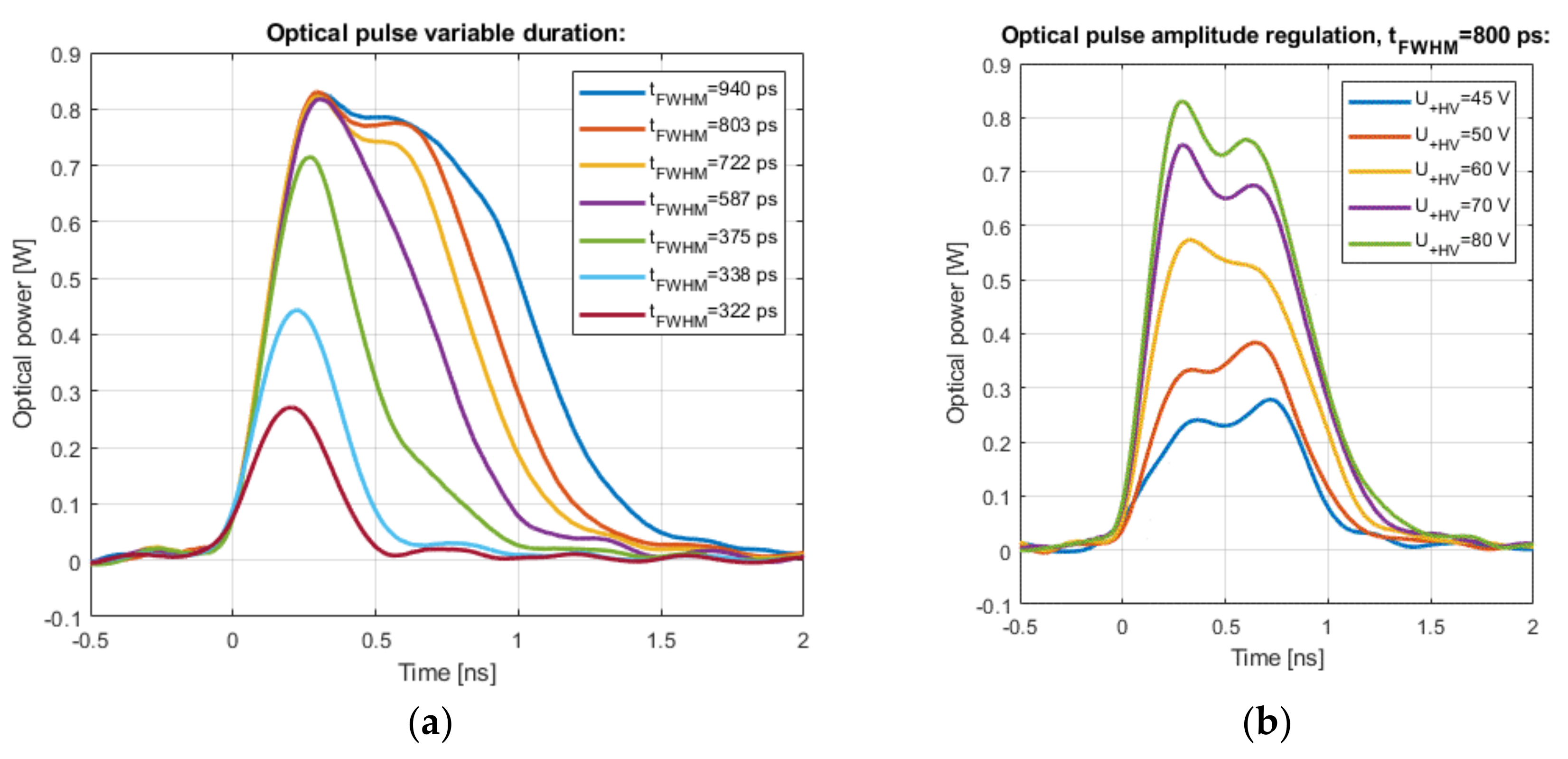
The effect of the pulse width regulation obtained with the designed driver is shown in Figure 9a. The shortest measured pulse has a symmetrical Gaussian shape and duration of 322 ps, which confirms the high-speed and high-current switching performance of the solution. The maximum pulse width is limited to 940 ps, because of the particular laser`s turn-on delay time. However, all measured optical pulses are characterized with rise time <220 ps and fall time <680 ps, which is much shorter than the laser manufacturer’s specification (see Table 2).
The optical pulse power regulation is shown in Figure 9b. The maximum pulsing current for U+HV = 80 V was measured to be approximately 1.3 A and is sufficient do drive most of the market-available 1 W NIR lasers.
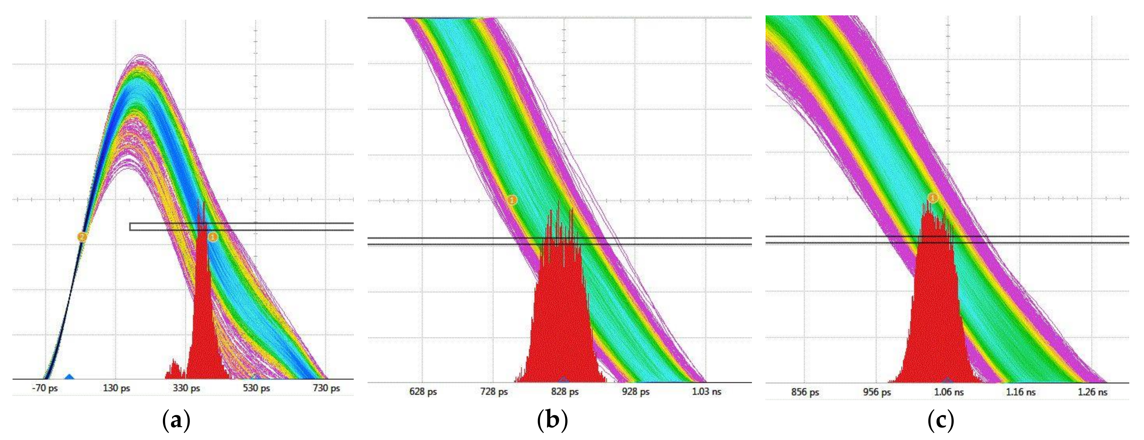
The measurements shown in Figure 9 prove that the developed laser driver is capable of independent regulation of the pulse width and amplitude, although one of the key parameters of the developed laser driver is a very low timing noise. In Figure 10a, family of time domain waveforms corresponding to multiple optical pulses generated by the laser diode are shown. The “blur” observed at the falling edges represents the phase fluctuations of the signal (noise in the time domain)—jitter. The maximum measured jitter is σt = 28 ps for tFWHM = 500 ps. This ensures stable and reproducible optical pulse generation, regardless of the width of the optical pulse.
The pulse-to-pulse optical signal amplitude stability measurements are shown in Figure 11. The amplitude fluctuations-over-time parameter σA (std. dev.) is not affected by tFWHM or frep adjustments. However, as listed in Table 3, the optical pulse amplitude instability increases with higher modulation currents. To present amplitude instability relative to peak pulse amplitude, the SA and SC parameters were included in Table 3. The SA ratio is not constant and, compared to the SC, measured with resistive load RL = 33 Ω; we suspect that both the NIR laser and detection system exhibit an additional 1/f or excess noise.
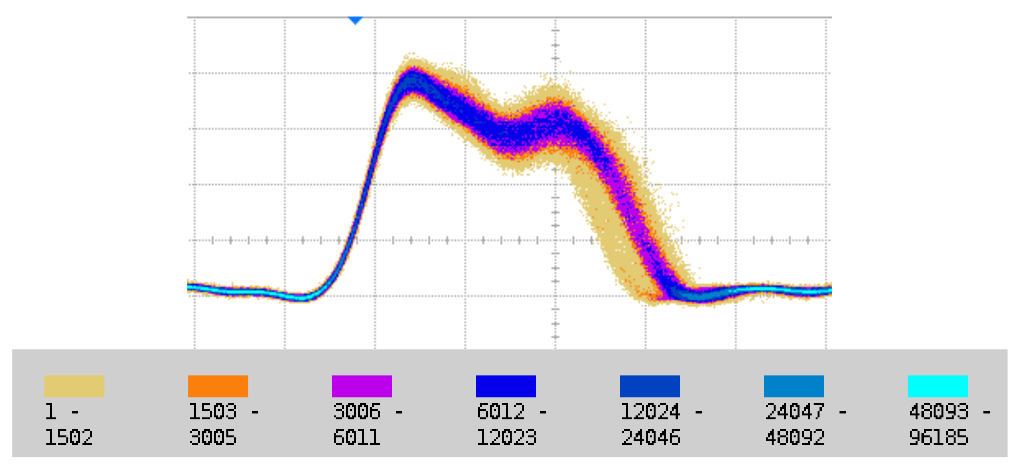
The long term stability was measured with an optical peak power of 750 mW and tFWHM = 750 ps, while the repetition rate was set to 1 MHz. Figure 12 presents the data set after 12 h of continuous optical signal sampling. The laser driver showed a high and reproducible performance with negligible pulse width and amplitude drift.
5. Conclusions
In this paper a new approach of utilizing delay-line based pulsed current source for generating short optical pulses was presented and described. With the use of modern HEMT transistors and modern reconfigurable device (FPGA), a fast and high-current switching driving stage was designed.
The novelty of the presented solution lies in the independence of the pulse width adjustment ranging from <300 ps to 2 ns and the peak pulse current adjustment (reaching up to Imax = 1.2 A), with the repetition rate form single-shot up to frep max = 20 MHz. Moreover, all the control and timing signals are sourced from the FPGA timing circuit, which makes the presented solution a complete, stand-alone device.
It was shown that the driver integrated with a NIR laser can generate high-power optical pulses with precisely adjusted amplitude and duration. Very low timing noise, amplitude reproducibility, and long-term stability has proven the high performance of the developed system.
Author Contributions
Conceptualization, M.Ż. and P.Z.W.; methodology, M.Ż. and P.Z.W.; software, P.Z.W.; validation, M.Ż.; formal analysis, P.Z.W.; investigation, M.Ż.; resources, P.Z.W; data curation, M.Ż.; writing—original draft preparation, M.Ż. and P.Z.W.; writing—review and editing, M.Ż. and P.Z.W.; visualization, M.Ż. and P.Z.W.; supervision, P.Z.W.; project administration, M.Ż.; funding acquisition, P.Z.W.
Funding
This research received no external funding.
Conflicts of Interest
The authors declare no conflict of interest.
References
- Hintikka, M.; Hallman, L.; Kostamovaara, J. Comparison of the leading-edge timing walk in pulsed TOF laser range finding with avalanche bipolar junction transistor (BJT) and metal-oxide-semiconductor (MOS) switch based laser diode drivers. Rev. Sci. Instrum. 2017, 88, 123109. [Google Scholar] [CrossRef] [PubMed]
- Glaser, J. High Power Nanosecond Pulse Laser Driver Using an GaN FET. In Proceedings of the PCIM Europe 2018, International Exhibition and Conference for Power Electronics, Intelligent Motion, Renewable Energy and Energy Management, Nuremberg, Germany, 5–7 June 2018; pp. 1–8. [Google Scholar]
- Masters, B.M. Fluorescence Lifetime Spectroscopy and Imaging: Principles and Applications in Biomedical Diagnostics. J. Biomed. Opt. 2014, 19, 119–121. [Google Scholar] [CrossRef]
- Walker, R.J. Quantum Cascade Laser Spectroscopy: Developments and Applications. Ph.D. Thesis, University of Oxford, Oxford, UK, 2011; pp. 17–51. [Google Scholar]
- Chen, S.; Sato, A.; Ito, T.; Yoshita, M.; Akiyama, H.; Yokoyama, H. Sub-5-ps optical pulse generation from a 1.55-µm distributed-feedback laser diode with nanosecond electric pulse excitation and spectral filtering. Opt. Express 2012, 20, 24843–24849. [Google Scholar] [CrossRef] [PubMed]
- Lanz, B. Compact Current Pulse-Pumped GaAs–AlGaAs Laser Diode Structures for Generating High Peak-Power (1–50 Watt) Picosecond-Range Single Optical Pulses. Ph.D. Thesis, University of Oulu, Oulu, Finland, 2016; pp. 47–83. [Google Scholar]
- Upadhyay, J.; Navathe, C.P. A fast high-voltage pulse generator wit variable amplitude and duration. Meas. Sci. Technol. 2006, 1, N25. [Google Scholar] [CrossRef]
- Żbik, M.; Wieczorek, P.Z. Versatile subnanosecond laser diode driver. Proc. SPIE 2016. [Google Scholar] [CrossRef]
- Miller, S.L.; Ebers, J.J. Alloyed junction avalanche transistors. Bell Syst. Techn. J. 1955, 34, 883–902. [Google Scholar] [CrossRef]
- Mohamad, S.; Tang, F.; Bermak, A.; Amira, A.; Benammar, M. A Low Power Temperature Sensor based on a Voltage to Time Converter Cell. In Proceedings of the 25th International Conference on Microelectronics (ICM), Beirut, Lebanon, 15–18 December 2013. [Google Scholar] [CrossRef]
- Osheroff, P.; Rue, G.S.L.; Gupta, S. A highly linear 4GS/s uncalibrated voltage-to-time converter with wide input range. In Proceedings of the 2016 IEEE International Symposium on Circuits and Systems (ISCAS), Montreal, QC, Canada, 22–25 May 2016; pp. 89–92. [Google Scholar]
- Kołodziejski, W.; Kuta, S.; Jasiełski, J. Current controlled delay line elements’ improvement study. In Proceedings of the International Conference on Signals and Electronic Systems (ICSES), Wroclaw, Poland, 18–21 September 2012. [Google Scholar]
- Xilinx. Available online: https://www.xilinx.com/support/documentation/data_sheets/ds160.pdf (accessed on 27 February 2019).
- Highland Technology. Available online: tps://www.highlandtechnology.com/DSS/T160DS.shtml (accessed on 28 February 2019).
- OSRAM Opto Semiconductors. Available online: https://www.osram.com/os/ecat/Radial%20T1%203-4%20SPL%20PL90/com/en/class_pim_web_catalog_103489/global/prd_pim_device_2220018/ (accessed on 27 February 2019).
- THORLABS. Available online: https://www.thorlabs.com/thorproduct.cfm?partnumber=DET08CFC (accessed on 27 February 2019).
Figure 1.
Simplified schematics of two basic pulsed laser diode drivers utilizing a single switching device: (a) The driver with a pulse shaping capacitor CC; (b) the driver with a pulse shaping delay line.
Figure 1.
Simplified schematics of two basic pulsed laser diode drivers utilizing a single switching device: (a) The driver with a pulse shaping capacitor CC; (b) the driver with a pulse shaping delay line.

Figure 2.
Simplified schematic of charge line dual-Field Effect Transistors (FET) laser diode driver.
Figure 2.
Simplified schematic of charge line dual-Field Effect Transistors (FET) laser diode driver.

Figure 3.
Two popular methods for the generation of a variable delay: (a) With the use of DDS, and (b) voltage-time conversion.
Figure 3.
Two popular methods for the generation of a variable delay: (a) With the use of DDS, and (b) voltage-time conversion.

Figure 4.
Block diagram of the Digital Clock Manager (DCM) delay block.

Figure 5.
Block diagram of the digital subsystem responsible for the trigger signal generation.

Figure 6.
PCBs of the pulsed laser driver system: (a) Dual-FET output stage; (b) Timing circuit (Field-Programmable Gate Array (FPGA)) PCB–ZTEX evaluation board with the Spartan 6 device.
Figure 6.
PCBs of the pulsed laser driver system: (a) Dual-FET output stage; (b) Timing circuit (Field-Programmable Gate Array (FPGA)) PCB–ZTEX evaluation board with the Spartan 6 device.
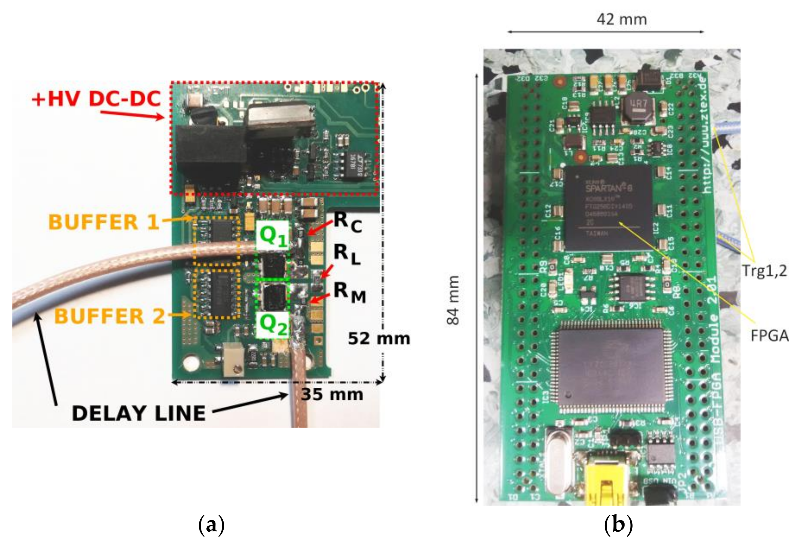
Figure 7.
Preliminary tests of the pulsed laser driver: (a) Pulse width regulation; (b) pulse peak current regulation.
Figure 7.
Preliminary tests of the pulsed laser driver: (a) Pulse width regulation; (b) pulse peak current regulation.

Figure 8.
The pulse amplitude compression as a function of repetition rate.

Figure 9.
Tests of the developed pulsed driver coupled with the NIR laser diode: (a) Pulse width regulation; (b) pulse peak current regulation.
Figure 9.
Tests of the developed pulsed driver coupled with the NIR laser diode: (a) Pulse width regulation; (b) pulse peak current regulation.

Figure 10.
Jitter measurements of three different optical pulse widths: (a) tFWHM = 500 ps, σt = 28 ps; (b) tFWHM = 750 ps, σt = 24 ps; (c) tFWHM = 1 ns, σt = 22 ps.
Figure 10.
Jitter measurements of three different optical pulse widths: (a) tFWHM = 500 ps, σt = 28 ps; (b) tFWHM = 750 ps, σt = 24 ps; (c) tFWHM = 1 ns, σt = 22 ps.

Figure 11.
Pulsed optical signal peak amplitude stability measured for tFWHM = 900 ps, frep = 1 MHz and peak power of: (a) 250 mW, σA = 6.5 mW; (b) 520 mW, σA = 17.3 mW; (c) 750 mW, σA = 28.6 mW.
Figure 11.
Pulsed optical signal peak amplitude stability measured for tFWHM = 900 ps, frep = 1 MHz and peak power of: (a) 250 mW, σA = 6.5 mW; (b) 520 mW, σA = 17.3 mW; (c) 750 mW, σA = 28.6 mW.
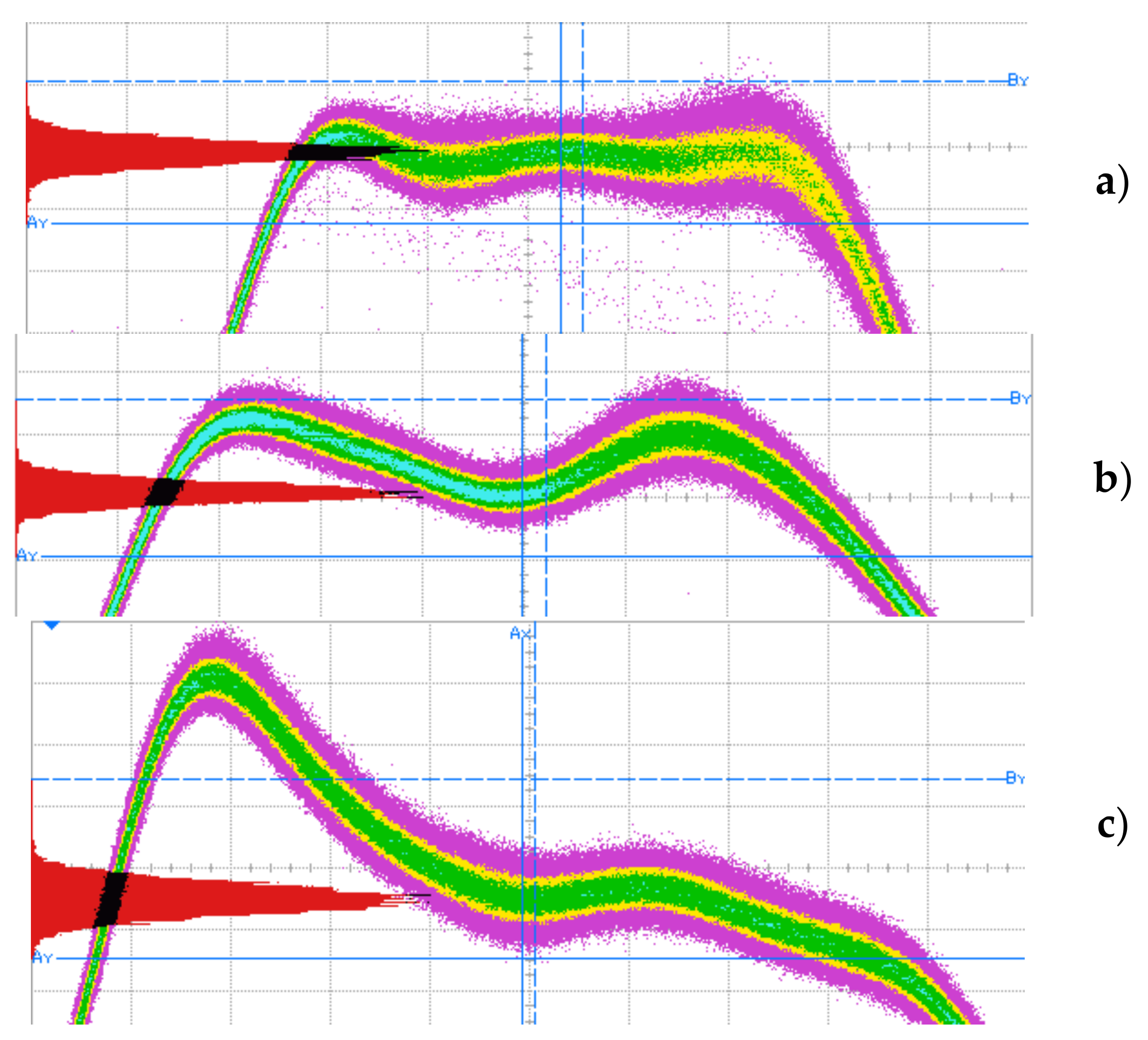
Figure 12.
Long term (12 h) pulse stability measurement. Infinite trace persistence with temperature grading was used. Horizontal axis 250 ps/div; vertical axis 250 mW/div. The legend describes the number of hits in the trace pixel.
Figure 12.
Long term (12 h) pulse stability measurement. Infinite trace persistence with temperature grading was used. Horizontal axis 250 ps/div; vertical axis 250 mW/div. The legend describes the number of hits in the trace pixel.

Table 1.
GaN High-Electron-Mobility Transistors (HEMT) electrical characteristics.
| Parameter | Rating |
|---|---|
| UDS MAX | 84 V |
| ID SAT (UDS = 6 V, UGS = 2 V) | 2 A |
| RDS ON | <2 Ω |
| Operation frequency | DC to 6 GHz |
| Pdiss max | 8 W |
Table 2.
Near Infra-Red (NIR) laser catalogue typical parameters (room temperature).
| Parameter | Symbol | Value |
|---|---|---|
| Threshold current | Ith | 0.75 A |
| Operating forward voltage | UF | 9 V |
| Wavelength | λpeak | 905 nm |
| Maximum output power | Po max | 75 W |
| Rise/fall time | tr/tf | 1 ns/1 ns |
Table 3.
Pulse-to-pulse amplitude stability (tFWHM = 900 ps, frep = 1 MHz).
| Optical Pulse Measurements | ||
|---|---|---|
| Amplitude [mW] | σA [mW] | SA = Amp./σA |
| 250 (U+HV = 45 V) | 6.5 | 38 |
| 520 (U+HV = 60 V) | 17.3 | 30 |
| 750 (U+HV = 80 V) | 28.6 | 26 |
| Electrical Pulse Measurements (RL = 33 Ω) | ||
| Amplitude [mA] | σC [mA] | Sc = Amp./σC |
| 510 (U+HV = 45 V) | 1.3 | 392 |
| 705 (U+HV = 60 V) | 1.8 | 391 |
| 960 (U+HV = 80 V) | 2.5 | 384 |
© 2019 by the authors. Licensee MDPI, Basel, Switzerland. This article is an open access article distributed under the terms and conditions of the Creative Commons Attribution (CC BY) license (http://creativecommons.org/licenses/by/4.0/).
Share and Cite
MDPI and ACS Style
Żbik, M.; Wieczorek, P.Z. Charge-Line Dual-FET High-Repetition-Rate Pulsed Laser Driver. Appl. Sci. 2019, 9, 1289. https://doi.org/10.3390/app9071289
AMA Style
Żbik M, Wieczorek PZ. Charge-Line Dual-FET High-Repetition-Rate Pulsed Laser Driver. Applied Sciences. 2019; 9(7):1289. https://doi.org/10.3390/app9071289
Chicago/Turabian StyleŻbik, Mateusz, and Piotr Zbigniew Wieczorek. 2019. "Charge-Line Dual-FET High-Repetition-Rate Pulsed Laser Driver" Applied Sciences 9, no. 7: 1289. https://doi.org/10.3390/app9071289
Note that from the first issue of 2016, this journal uses article numbers instead of page numbers. See further details here.